Strain-engineered inverse charge-funnelling in layered semiconductors
The control of charges in a circuit due to an external electric field is ubiquitous to the exchange, storage and manipulation of information in a wide range of applications, from electronic circuits to synapses in neural cells1. Conversely, the ability to grow clean interfaces between materials has been a stepping stone for engineering built-in electric fields largely exploited in modern photovoltaics and opto-electronics2. The emergence of atomically thin semiconductors3 is now enabling new ways to attain electric fields and unveil novel charge transport mechanisms. Here, we report the first direct electrical observation of the inverse charge-funnel effect4, 5 enabled by deterministic and spatially resolved strain-induced electric fields in a thin sheet of HfS2. We demonstrate that charges driven by these spatially varying electric fields in the channel of a phototransistor lead to a enhancement in the responsivity. These findings could enable the informed design of highly efficient photovoltaic cells.
The development of novel ways to tailor the electrical and optical properties of atomically thin semiconductors, for example by local modification of their composition6, 7 or structure8, holds the promise to explore new implementations of electric fields and unveil novel mechanisms of charge transport which can boost the efficiency of opto-electronic devices. The application of strain is one original way to engineer electric fields in semiconducting materials through a varying energy gap. However, common bulk semiconductors can only sustain strain of the order of without rupture9, a value which limits the range of novel physical phenomena and applications that can be accessed. On the contrary, layered semiconductors, such as graphene10 and transition metal dichalcogenides (TMDs)11, are theoretically predicted to be able to sustain record high levels of strain 12, 13 expected to lead to an unprecedented tunability of their energy gap by more than 14. One tantalizing charge transport phenomenon which could be accessible owing to large values of strain is the funneling of photoexcited charges away from the excitation region and towards areas where they can be efficiently extracted4, 15, 16. Such effect is heralded as a gateway for a new generation of photovoltaic devices with efficiencies that could approach the thermodynamic limit2, 4.
In general, strain-induced gradients of energy gaps create a force on (neutral) excitons that pushes them towards the regions with the smallest energy gap. In direct gap semiconductors, this area corresponds to that of maximum tension. Hence, the strain pattern generated by simply poking a sheet of direct gap TMD would normally funnel the charges towards the apex of the wrinkle4, 15, 17, 18. Consequently, the extraction of the charges for energy harvesting or sensing poses considerable technological challenges and for this reason the funneling effect has not yet been observed experimentally in electrical transport. On the other hand, the opposite behaviour is theoretically expected in some indirect gap semiconductors (e.g. HfS2 and HfSe2) and in black-phosphorus, where the energy gap increases in the regions of tension14. This would allow the exploitation of the so-called inverse charge funnelling5 whereby a strain pattern generated by poking a sheet of these materials would push the charges away from the apex of the wrinkle, making them readily available for energy harvesting or computing purposes to an external circuit.
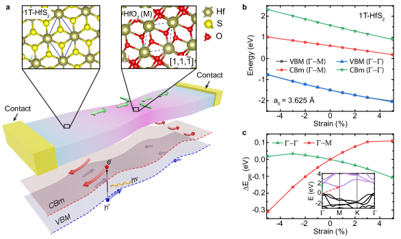
In traditional semiconductors such as Si and Ge, strain is typically introduced at the growth stage by dislocations or elemental composition19. These techniques do not easily allow the creation of complex planar strain patterns, forbidding the development of ultra-thin charge-funnel devices. These limitations can be overcome by using atomically thin semiconductors, such as HfS2. In this case, specific strain patterns can potentially be engineered in the plane of the TMDC by exploiting the lattice mismatch between the semiconductor and its in-situ grown oxide, see figure 1a. Ab initio DFT calculations suggest that the cleavage plane of monoclinic HfO2 has a spatial arrangement of \ceHf atoms commensurate to that of the basal plane of HfS2, with an Hf-Hf distance of . Since the Hf-Hf distance in HfS2 is , a transition between these two structures is likely to introduce an average compressive strain in the semiconductor at the interface with its oxide. Hence, anchoring the TMD at the edges, for example by depositing electrical contacts20, would allow the same amount of strain to be induced away from the oxidised area in the opposite direction (green arrows in figure 1a). Such tensile strain pattern results in the spatial modulation of the bandgap of HfS2 and therefore the creation of spatially varying electric fields, which are the key ingredients to observe the inverse charge funnel effect. The magnitude of these electric fields can be determined from the change in the energy gap with strain. This has been calculated using DFT and the results, shown in figure 1b-c, predict an increasing (decreasing) value of the direct gap () with compressive (tensile) strain whilst the indirect gap () behaves the opposite.
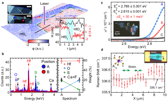
To engineer strain-induced electric fields through lattice mismatch we employ a spatially resolved photo-oxidation technique. Upon exposure to a focussed laser ( nm, MW/cm2) we find that HfS2 is readily oxidized, becoming invisible to the naked eyes (see figure 2a). Surprisingly, topographic atomic force microscopy (AFM) measurements show no ablation of the material in the laser-exposed area while the tapping phase image clearly reveals a change in its viscoelastic properties (see also supplementary section S2.1). The energy dispersive X-ray microanalysis (EDXMA) shows the absence of the \ceS peaks (K lines) and the appearance of an \ceO peak (Kα line) in the laser-irradiated areas. This is in stark contrast to the spectrum of the pristine HfS2 where the expected S peaks are clearly measured and no O peak is resolved (figure 1b). No change is observed in the Hf and substrate peaks. Quantitative analysis shows that, upon laser irradiation, the weight ratio of S decreases from to of the total, while the O content increases from to , indicating the formation of HfO2. Furthermore, the oxidized area is compatible with the diffraction-limited spot size of our laser system (see figure S1d,e), indicating that a photon-assisted oxidation process, as opposed to a thermally driven one, is taking place.
The photo-oxidation of 2D semiconductors has recently been shown to depend on the rate of charge-transfer between the surface of the material and the aqueous oxygen present in air21 via the oxygen-water redox couple \ce2 H2O ¡=¿ O2(aq) + 4 e^- + 4 H^+, where the O2 binds to a metal site22. Adopting the same model and supported by the EDXMA data, we summarize the oxidation reaction of HfS2 as \ceHfS2(s) + 3 O2(aq) + hν -¿ HfO2(s) + 2 SO2(g). Here, the absorption of a photon of energy h produces an optical excitation in the \ceHfS2, leaving it in an excited state (\ceHfS2 + hν -¿ HfS2^*) which provides free carriers that are transferred to the oxygen on the surface, producing an oxygen radical ion \ceO2^.-(aq) which reacts with the \ceHfS2 (see supplementary section S1 for details). The feasibility of the proposed reaction is confirmed by DFT calculations, which show an energy cost of eV per \ceHfS2 molecule (see supplementary section S3.1). Indeed, a detailed study of the oxidation rate and its dependence on the laser flux and the initial amount of pristine material confirms that the process is described by the Mercus-Gerischer theory21 as expected for photo-oxidation (see supplementary equation ()S4) and supplementary figure S1b,c).
Theoretically, we expect that a compressive strain should induce a change by as much as meV in the bandgap of \ceHfS2 (figure 1c). Indeed, a measurement of the absorption coefficient , in the region close to the laser-written oxide, confirms an energy gap difference of (see figure 2c). The absorption coefficient measured in the centre of the oxidised area is close to zero, showing that the direct absorption edge lies above , as expected for HfO2. Raman spectroscopy allows us to map the strain profile induced in a clamped device, as shown in figure 2d inset. First-principle studies have shown that the peak corresponding to the Raman-active A1g phonon mode of HfS2 downshifts (upshifts) with the application of tensile (compressive) strain23. In figure 2d we plot the frequency of such mode as a function of position along the length of the device. The experimental frequency of the A1g mode of pristine multi-layer HfS2 is found to be from the measurements reported in figure S1c-d, in good agreement with literature24. The deviation of the measured peak from this value demonstrates the presence of compressive and tensile strain along the device (green arrows in figure 2d), compatible with the model proposed in figure 1a (the data have been calibrated using the position of two fixed peaks to compensate for instrumental shifts, as explained in the methods section).
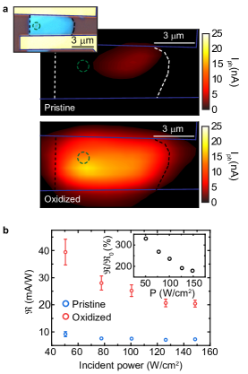
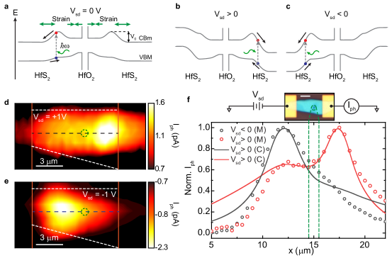
Demonstrating the creation of strain gradients using a spatially resolved photo-oxidation process allows the realisation of novel planar heterointerfaces and energy band tailoring. Hence, we employed scanning photocurrent microscopy (SPCM) mapping25, 26 to study the photoresponse of a strain-engineered HfS2 photodetector in a field effect transistor (FET) configuration in search of the inverse charge funneling effect. Figure 3a shows the SPCM maps before and after photo-oxidation of a single spot in the channel of the FET. We observe an enhancement of the photoresponse close to the laser-oxidised area, where the responsivity increases by at low powers and by at the saturation power ( W/cm2), as detailed in figure 3b. In order to correlate this observation with the electrical detection of charge funnelling, we perform SPCM in the device presented in figure 2d. Figure 4a schematically depicts the band alignment in such device for an applied bias V, where the changes in the valence band maximum (VBM) and conduction band minimum (CBm) with strain are taken from figure 1b for indirect transitions (based on the data from Raman and absorption spectroscopy). Excited electron-hole pairs, in the proximity of the strained area, are funnelled towards the electrodes by the built-in energy gradient, giving an enhanced photoresponse4, 5. For , both sides of the strained junction will give equal contribution. Indeed, we were not able to measure any photoresponse in absence of a bias, see also Supplementary figure S9. The application of a source-drain bias larger than the difference between the conduction band energy at the maximum strain point and its value in the unstrained region () is expected to exhibit a larger photoresponse in regions with maximal energy gradients (see also supplementary figure S7d). This is indeed observed in the SPCM map shown in figure 4d. Furthermore, by reversing the bias it is possible to mirror the profile of the built-in electric field and consequently reflect the position of the maximum photoresponse, see figures 4c and 4e.
To fully capture the role of the inverse charge funneling effect on the measured photoresponse we develop a one-dimensional analytical model. For simplicity we assume that the strain gradient induces a built-in potential which decays linearly with the distance from the strain junction, creating a local built-in electric field (see supplementary equation (S11)). By solving the charge continuity equation (see supplementary section S5), assuming the rate of carrier generation to be a delta function at the illumination point , we find that the charge density as a function of position is given by:
| (1) |
where is the excited carrier density at the injection point, is the temperature, is the Boltzmann constant, is the electron charge, is the carriers lifetime, is the diffusion coefficient and is the electric field due to the applied bias. The plus (minus) sign applies to the left (right) strain-engineered region, respectively and outside those regions. Calculating the current generated by this charge density distribution (see LABEL:eq:Current_SolutionGen) by scanning the laser along the channel, we can describe experimentally measured SPCM (see figure 4f). Although the strain gradient, and thus the built-in field, should be treated as , our simple assumptions allow the derivation of an analytical result which is still able to reproduce well the experimental data with as the only free fitting parameter. In our case we find a value of outside the strain region, which is typical of multi-layer semiconducting TMDs27. In the strain region we find , which translates in a carrier diffusion length of (assuming a mobility of )28. The observation of a diffusion length which exceeds the extension of the strained region () is, indeed, a signature of efficient separation and extraction of charges, compatible with the charge-funnel effect15. Future studies of the effects of bandgap engineering on the carriers recombination lifetimes could elucidate the physical mechanisms behind this improvement and may shed light on the role of hot-carriers in such strained devices for photovoltaic applications. In particular, charge funneling could allow carriers excited above the bandgap to be extracted before their excess kinetic energy is lost through cooling, enabling solar cells relying on this phenomena to overcome the Shockley-Queisser limit and bring their efficiency above 29. Furthermore, the spatial modulation of the semiconductor bandgap could be used to create an effective tandem solar cell, which would be able to absorb a much larger portion of the solar spectrum compared to a single bandgap device2, see also discussion in Supplementary section S6.
In summary, in this work we report the first experimental observation of the inverse charge funneling effect, that is a novel microscopic charge transport mechanism enabled by strain-induced electric fields. By developing a unique technique of photo-oxidation, we are able to engineer deterministic and spatially resolved strain patterns in ultra-thin films of HfS2 which in return generate built-in electric fields. Such strain gradient is responsible for the enhancement of the responsivity of a phototransistor of up to , which was attributed to the inverse charge funnel effect. A simple analytical model was derived to simulate the scanning photocurrent microscopy experiments, which demonstrated the charge funneling effect and allowed the determination of a long carrier recombination lifetime of in the strain-engineered region of the device. These results open the route towards the exploitation of strain-engineered devices for high-efficiency energy harvesting and sensing applications, with the potential to overcome the intrinsic limitations of current solar cells by exploiting both hot-carriers extraction and lossless transport, to achieve efficiencies approaching the thermodynamic limit in photovoltaic devices2, 29. The use of atomically thin materials could open the door to the incorporation of such devices in emerging wearable electronics technologies30 and smart buildings31, creating a new paradigm in energy harvesting.
Methods
Sample preparation
Thin flakes of \ceHfS2 were obtained by micro-mechanical exfoliation32 from commercial bulk crystal on different substrates. The oxygen free CaF2 substrate was used in the EDXMA allowing one to probe purely the oxygen peak of the oxidised HfS2. This same substrate was used for Raman spectroscopy since it only has a well-defined Raman peak at cm-1. Quartz ( m thick) substrate was used to perform the absorption coefficient measurements, due to its constant refractive index across the scanned energy range. Substrates of heavily doped \ceSi capped with nm of thermally grown \ceSiO2 were used to fabricate phototransistors using standard electron-beam lithography, deposition of Ti/Au (/ nm) for the contacts followed by lift-off in Acetone. For EDXMA analysis the sample was coated with nm of \ceAu and grounded to avoid charging of the \ceCaF2 substrate. The choice of substrate did not affect the laser-induced oxidation in terms of morphology, exposure time or incident power.
Atomic force microscopy and energy-dispersive X-ray microanalysis
Atomic force microscope (AFM) topography and phase image were acquired with a Bruker Innova AFM system, operating in the tapping (or dynamic) mode to avoid damage to the sample while maintaining a high spatial resolution. The measurements were done using a highly doped silicon tip acquired from Nanosensors with a nominal resonance frequency of kHz, and a sharp radius of curvature ( nm). Energy dispersive X-ray microanalysis (EDXMA) was performed using a Hitachi S-3200N scanning electron microscope equipped with an Oxford Instruments EDS Model 7021 (detection area mm2 and resolution at keV of eV). The accelerating voltage was kV and the total counts were fixed at for each spectrum. The observed \ceHf/\ceS weight ratio () in the pristine area, confirmed the stoichiometry of \ceHfS2, as also reported in the literature33.
Raman and optical spectroscopy
Raman spectroscopy of ultrathin HfS2 requires great care in order to avoid the photo-oxidation of the material: low laser intensity, long acquisition time and low background noise are required. For this reason the Raman spectra presented in this work were acquired with a custom-built micro-Raman spectrometer25. For very thin flakes we used an incident power density of kW/cm2 with an acquisition time of s, with no visible changes in the sample. The same set-up was also used to acquire the transmission and reflection spectra, in order to measure the absorption coefficient, with an incandescent bulb and a white LED as light sources. All light sources were thermally controlled to ensure no thermal drift during measurements.
In order to determine with great accuracy the Raman shift of the A1g mode of HfS2 we calibrated the acquired spectra relying on the presence of two fixed peaks which were acquired in the same spectrum: the silicon peak (from the substrate) and the spurious laser-line peak (L) which appear at and , respectively (see figure S1b and S2h). Since these two peaks do not belong to the HfS2 they will not shift with the strain applied to the semiconductor and can be used to correct for instrumental shifts of the frequency.
Determination of the absorption coefficient
The absorption coefficient is defined as the fraction of the power absorbed per unit length in the medium, and it is a strong function of the incident wavelength . We used the formulation by Swanepoel34 to calculate the absorption coefficient of \ceHfS2 and \ceHfO225. In order to account for the interface between the \ceHfS2 and the substrate we used the measured reflectance of a thick \ceHfS2, so that we can ignore multiple reflections from the substrate, to compute the refractive index of \ceHfS2. We found that across the measured range and, thus (reflectance at air/medium interface). Since (air/quartz interface), we assumed in equation (A3) in reference 34. The same result can be obtained by computing from the measured transmittance curve, using equation (20) in reference 34. The bandgap of a semiconductor is related to the absorption coefficient by: for direct allowed transitions35, therefore measurement of close to the absorption edge can be used to extrapolate the value of the direct bandgap of \ceHfS2.
Photoresponse and scanning photocurrent microscopy measurements
In our custom made multi-functional opto-electronic set-up, solid-state diode lasers are used and all the optical components are chosen in order to minimize deviations from the TEM00 laser mode25, which has a Gaussian intensity distribution. The lasers spot diameter and depth of focus are: for nm, nm and nm; for nm, nm and nm; for nm, nm and nm.
Scanning photocurrent maps were acquired by measuring the photo-generated current at each laser spot location ( nm, W/cm2, see supplementary section S4 for detailed electrical characterization). The electrical signal from the device was amplified with a DL Model 1211 current preamplifier and measured with an Ametek Model 7270 DSP Lock-in amplifier. The locking frequency was provided by a mechanical chopper which modulated the light source. The bias and gate voltages were provided by a Keithley 2400 SourceMeter.
Band structure calculations
First principles simulations were carried out using the density functional by Perdew, Burkeand Ernzerhof (PBE)36, as implemented in the QUANTM ESPRESSO package37. The total energy of the system was minimized with respect to coordinates of all atoms and the cell parameters for the bulk structures and the ground state obtained. For bulk, the structure was allowed to fully relax using the Broyden-Fletcher-Goldfarb-Shanno (BFGS) algorithm. A cutoff of Ry and a Monkhorst-Pack k-point set were used for these calculations. Based upon these total energy calculations, reaction energetics were calculated. The reaction was taken as \ceHfS2(s,2D) + 3O2(g) -¿ HfO2(s) + 2SO2(g), where the energy of the reaction is calculated from . The \ceHfO2 structure was fully relaxed.
Acknowledgements
The authors would like to thank R. Keens for support with the DFT calculations; M. D. Barnes and G. F. Jones for insightful discussion. Funding: S. Russo and M.F. Craciun acknowledge financial support from EPSRC (Grant no. EP/K017160/1, EP/K010050/1, EP/M001024/1, EP/M002438/1), from Royal Society international Exchanges Scheme 2016/R1, from European Commission (FP7-ICT-2013-613024-GRASP) and from The Leverhulme trust (grant title ”Quantum Revolution” and ”Quantum Drums”). I. Amit received funding from the People Programme (Marie Curie Actions) of the European Union’s Eighth Framework Programme Horizon 2020 under REA grant agreement number 701704. S. Hepplestone acknowledges the use of the resources allocated by the MCC via membership of the UK’s HEC Materials Chemistry Consortium, funded by EPSRC (EP/L000202), this work used the ARCHER UK National Supercomputing Service. Author contributions: A.D.S. conceived the idea, designed the experiment, performed the optical and electrical measurements. I.A. carried out the AFM measurements. S.P.H. carried out the DFT calculations. M.F.C. and S.R. supervised the project. All authors discussed the interpretation of the results and contributed to the writing of the paper. Competing financial interests The authors declare no competing financial interests. Data and materials availability: All data needed to evaluate the conclusions in the paper are present in the main text and/or the Supplementary Materials. Additional data related to this paper may be requested from the authors. Correspondence and requests for materials should be addressed to S.R.
References
- Indiveri and Liu 2015 Indiveri, G.; Liu, S. C. Memory and Information Processing in Neuromorphic Systems. Proceedings of the IEEE 2015, 103, 1379–1397
- Nelson 2011 Nelson, J. The Physics of Solar Cells, 1st ed.; Imperial College Press, 2011; Chapter 10, pp 289–325
- Chhowalla et al. 2013 Chhowalla, M.; Shin, H. S.; Eda, G.; Li, L.-J.; Loh, K. P.; Zhang, H. The chemistry of two-dimensional layered transition metal dichalcogenide nanosheets. Nat Chem 2013, 5, 263–275
- Feng et al. 2012 Feng, J.; Qian, X.; Huang, C.-W.; Li, J. Strain-engineered artificial atom as a broad-spectrum solar energy funnel. Nat Photon 2012, 6, 866–872
- San-Jose et al. 2016 San-Jose, P.; Parente, V.; Guinea, F.; Roldán, R.; Prada, E. Inverse Funnel Effect of Excitons in Strained Black Phosphorus. Phys. Rev. X 2016, 6, 031046
- Yang et al. 2017 Yang, K.; Wang, X.; Li, H.; Chen, B.; Zhang, X.; Li, S.; Wang, N.; Zhang, H.; Huang, X.; Huang, W. Composition- and phase-controlled synthesis and applications of alloyed phase heterostructures of transition metal disulphides. Nanoscale 2017, 9, 5102–5109
- De Sanctis et al. 2017 De Sanctis, A.; Jones, G. F.; Wehenkel, D. J.; Bezares, F.; Koppens, F. H. L.; Craciun, M. F.; Russo, S. Extraordinary linear dynamic range in laser-defined functionalized graphene photodetectors. Science Advances 2017, 3
- Li et al. 2016 Li, Y.; Duerloo, K.-A. N.; Wauson, K.; Reed, E. J. Structural semiconductor-to-semimetal phase transition in two-dimensional materials induced by electrostatic gating. Nat Comm 2016, 7, 10671
- Cheng et al. 2010 Cheng, T.-H.; Peng, K.-L.; Ko, C.-Y.; Chen, C.-Y.; Lan, H.-S.; Wu, Y.-R.; Liu, C. W.; Tseng, H.-H. Strain-enhanced photoluminescence from Ge direct transition. Applied Physics Letters 2010, 96
- Novoselov et al. 2004 Novoselov, K. S.; Geim, A. K.; Morozov, S. V.; Jiang, D.; Zhang, Y.; Dubonos, S. V.; Grigorieva, I. V.; Firsov, A. A. Electric Field Effect in Atomically Thin Carbon Films. Science 2004, 306, 666–669
- Wang et al. 2012 Wang, Q. H.; Kalantar-Zadeh, K.; Kis, A.; Coleman, J. N.; Strano, M. S. Electronics and optoelectronics of two-dimensional transition metal dichalcogenides. Nat Nano 2012, 7, 699–712
- Lee et al. 2008 Lee, C.; Wei, X.; Kysar, J. W.; Hone, J. Measurement of the Elastic Properties and Intrinsic Strength of Monolayer Graphene. Science 2008, 321, 385–388
- Bertolazzi et al. 2011 Bertolazzi, S.; Brivio, J.; Kis, A. Stretching and Breaking of Ultrathin MoS2. ACS Nano 2011, 5, 9703–9709
- Guzman and Strachan 2014 Guzman, D. M.; Strachan, A. Role of strain on electronic and mechanical response of semiconducting transition-metal dichalcogenide monolayers: An ab-initio study. Journal of Applied Physics 2014, 115, 243701
- Castellanos-Gomez et al. 2013 Castellanos-Gomez, A.; Roldán, R.; Cappelluti, E.; Buscema, M.; Guinea, F.; van der Zant, H. S. J.; Steele, G. A. Local Strain Engineering in Atomically Thin MoS2. Nano Letters 2013, 13, 5361–5366
- Li et al. 2015 Li, H.; Contryman, A. W.; Qian, X.; Ardakani, S. M.; Gong, Y.; Wang, X.; Weisse, J. M.; Lee, C. H.; Zhao, J.; Ajayan, P. M.; Li, J.; Manoharan, H. C.; Zheng, X. Optoelectronic crystal of artificial atoms in strain-textured molybdenum disulphide. Nature Communications 2015, 6, 7381, Article
- Manzeli et al. 2015 Manzeli, S.; Allain, A.; Ghadimi, A.; Kis, A. Piezoresistivity and Strain-induced Band Gap Tuning in Atomically Thin MoS2. Nano Letters 2015, 15, 5330–5335
- Yang et al. 2015 Yang, S.; Wang, C.; Sahin, H.; Chen, H.; Li, Y.; Li, S.-S.; Suslu, A.; Peeters, F. M.; Liu, Q.; Li, J.; Tongay, S. Tuning the Optical, Magnetic, and Electrical Properties of ReSe2 by Nanoscale Strain Engineering. Nano Letters 2015, 15, 1660–1666
- Lee et al. 2005 Lee, M. L.; Fitzgerald, E. A.; Bulsara, M. T.; Currie, M. T.; Lochtefeld, A. Strained Si, SiGe, and Ge channels for high-mobility metal-oxide-semiconductor field-effect transistors. Journal of Applied Physics 2005, 97, 011101
- Shioya et al. 2014 Shioya, H.; Craciun, M. F.; Russo, S.; Yamamoto, M.; Tarucha, S. Straining Graphene Using Thin Film Shrinkage Methods. Nano Letters 2014, 14, 1158–1163
- Favron et al. 2015 Favron, A.; Gaufres, E.; Fossard, F.; Phaneuf-LflHeureux, A.-L.; Tang, N. Y.-W.; Levesque, P. L.; Loiseau, A.; Leonelli, R.; Francoeur, S.; Martel, R. Photooxidation and quantum confinement effects in exfoliated black phosphorus. Nat Mater 2015, 14, 826–832
- Jaegermann and Schmeisser 1986 Jaegermann, W.; Schmeisser, D. Reactivity of layer type transition metal chalcogenides towards oxidation. Surface Science 1986, 165, 143 – 160
- Chen 2016 Chen, J. Phonons in bulk and monolayer HfS2 and possibility of phonon-mediated superconductivity: A first-principles study. Solid State Communications 2016, 237, 14 – 18
- Cingolani et al. 1987 Cingolani, A.; Lugará, M.; Scamarcio, G.; Lévy, F. The Raman scattering in hafnium disulfide. Solid State Communications 1987, 62, 121 – 123
- De Sanctis et al. 2017 De Sanctis, A.; Jones, G. F.; Townsend, N. J.; Craciun, M. F.; Russo, S. An integrated and multi-purpose microscope for the characterization of atomically thin optoelectronic devices. Review of Scientific Instruments 2017, 88, 055102
- Graham and Yu 2013 Graham, R.; Yu, D. Scanning Photocurrent Microscopy in Semiconductor Nanostructures. Modern Physics Letters B 2013, 27, 1330018
- Kumar et al. 2013 Kumar, N.; He, J.; He, D.; Wang, Y.; Zhao, H. Charge carrier dynamics in bulk MoS2 crystal studied by transient absorption microscopy. Journal of Applied Physics 2013, 113, 133702
- Xu et al. 2015 Xu, K.; Wang, Z.; Wang, F.; Huang, Y.; Wang, F.; Yin, L.; Jiang, C.; He, J. Ultrasensitive Phototransistors Based on Few-Layered HfS2. Advanced Materials 2015, 27, 7881–7887
- Ross and Nozik 1982 Ross, R. T.; Nozik, A. J. Efficiency of hot?carrier solar energy converters. Journal of Applied Physics 1982, 53, 3813–3818
- Neves et al. 2015 Neves, A. I. S.; Bointon, T. H.; Melo, L. V.; Russo, S.; de Schrijver, I.; Craciun, M. F.; Alves, H. Transparent conductive graphene textile fibers. Scientific Reports 2015, 5, 9866
- Baetens et al. 2010 Baetens, R.; Jelle, B. P.; Gustavsen, A. Properties, requirements and possibilities of smart windows for dynamic daylight and solar energy control in buildings: A state-of-the-art review. Solar Energy Materials and Solar Cells 2010, 94, 87 – 105
- Novoselov et al. 2005 Novoselov, K. S.; Jiang, D.; Schedin, F.; Booth, T. J.; Khotkevich, V. V.; Morozov, S. V.; Geim, A. K. Two-dimensional atomic crystals. Proceedings of the National Academy of Sciences of the United States of America 2005, 102, 10451–10453
- Conroy and Park 1968 Conroy, L. E.; Park, K. C. Electrical properties of the Group IV disulfides, titanium disulfide, zirconium disulfide, hafnium disulfide and tin disulfide. Inorganic Chemistry 1968, 7, 459–463
- Swanepoel 1983 Swanepoel, R. Determination of the thickness and optical constants of amorphous silicon. Journal of Physics E: Scientific Instruments 1983, 16, 1214
- Fox 2010 Fox, M. Optical Properties of Solids; Oxford University Press, 2010
- Perdew et al. 1996 Perdew, J. P.; Burke, K.; Ernzerhof, M. Generalized Gradient Approximation Made Simple. Phys. Rev. Lett. 1996, 77, 3865–3868
- Giannozzi et al. 2009 Giannozzi, P. et al. QUANTUM ESPRESSO: a modular and open-source software project for quantum simulations of materials. Journal of Physics: Condensed Matter 2009, 21, 395502