Excitonic structure of the optical conductivity in MoS2 monolayers
Abstract
We investigate the excitonic spectrum of MoS2 monolayers and calculate its optical absorption properties over a wide range of energies. Our approach takes into account the anomalous screening in two dimensions and the presence of a substrate, both cast by a suitable effective Keldysh potential. We solve the Bethe-Salpeter equation using as a basis a Slater-Koster tight-binding model parameterized to fit the ab initio MoS2 band structure calculations. The resulting optical conductivity is in good quantitative agreement with existing measurements up to ultraviolet energies. We establish that the electronic contributions to the C excitons arise not from states at the point, but from a set of -points over extended portions of the Brillouin zone. Our results reinforce the advantages of approaches based on effective models to expeditiously explore the properties and tunability of excitons in TMD systems.
pacs:
72.80.Ga, 71.35.Cc, 11.10.StI Introduction
The widespread availability of bulk trigonal molybdenum disulfide (MoS2) has made this material one of the most widely studied transition metal dichalcogenides (TMDs) — especially at the strict monolayer thickness —, and has propelled MoS2 to one of the most prominent members of the family of semiconducting two-dimensional materials beyond graphene Wang et al. (2012); Geim and Grigorieva (2013); Butler et al. (2013); Choi et al. (2017); Wang et al. (2017a). In parallel with the interest and continued advances in optimizing sample production and transport characteristics, MoS2 and other closely related TMDs are of great appeal for optoelectronic applications Wang et al. (2012); Choi et al. (2017); Wang et al. (2017a). This has sustained intensive research to understand the processes that govern the electronic response of these crystals to light. Much progress has been made theoretically Komsa and Krasheninnikov (2012); Berghäuser and Malic (2014); Molina-Sánchez et al. (2013); Berkelbach et al. (2013); Qiu et al. (2013); Trolle et al. (2014); Zhang et al. (2014a); Wu et al. (2015); San-Jose et al. (2016); Chaves et al. (2017); Trushin et al. (2017); Selig et al. (2016); Wang et al. (2017b); Grüning and Attaccalite (2014); Glazov et al. (2017); Rhim et al. (2015); Wang and Guo (2015) and experimentally Mak et al. (2010); Splendiani et al. (2010); Li et al. (2013); Zhang et al. (2014b, a); Li et al. (2014); Dhakal et al. (2014); Miwa et al. (2015); Hill et al. (2015); Klots et al. (2014); Rigosi et al. (2016); Aleithan et al. (2016); Chiu et al. (2015); Selig et al. (2016); Chiu et al. (2015); Kumar et al. (2013); Clark et al. (2014); Mishina et al. (2015); Trolle et al. (2015); Säynätjoki et al. (2016); Woodward et al. (2017); Yin et al. (2014); Zhang et al. (2015) in both understanding fundamental properties and exploring the potential practical uses of these materials in devices.
As in nearly all strictly two-dimensional materials, MoS2 monolayers have a highly tunable carrier density Butler et al. (2013); Liu et al. (2017); Saito et al. (2016); Wang et al. (2015) and are amenable to having a number of properties tailored on-demand by different external procedures, including the customization of the optical band-gap Raja et al. (2017). It was early recognized that the intrinsic two-dimensionality and semiconducting character of TMDs bring about enhanced Coulomb interactions which, not only renormalize the electronic band structure with quantitative consequences for all derived single-particle processes, but also give rise to the strongest excitonic effects seen to date in the optical response of semiconductors Nakajima et al. (1980); Roldán et al. (2017); Ugeda et al. (2014). With binding energies as high as eV Komsa and Krasheninnikov (2012); Berghäuser and Malic (2014); Berkelbach et al. (2013); Qiu et al. (2013); Trolle et al. (2014); Wu et al. (2015); San-Jose et al. (2016); Chaves et al. (2017); Zhang et al. (2014b, a); Hill et al. (2015); Klots et al. (2014); Rigosi et al. (2016); Chiu et al. (2015) (depending on the strength of the interaction due to the sensitivity to their environment) and carrying a large spectral weight Qiu et al. (2013); Li et al. (2014); Mak et al. (2010), these two-particle excitations determine and dominate the optical response of TMD materials. As a result, excitons are now understood as a critical ingredient in any reliable theory and model of the optical properties of TMDs, to the extent that any theory that does not account for excitonic effects fails to capture even the most basic qualitative features of the optical gap and/or spectral weight distribution.
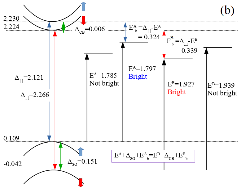
Monolayers of semiconducting TMDs are also interesting due to a number of other fundamental and unique features of their electronic structure that can broaden their range of applicability in optoelectronics. For example, the strong spin-orbit (SO) coupling splits the valence bands at the point by a large amount () which generates two families of excitons Miwa et al. (2015) [see A and B excitons in Fig. 1(b)] and allows the selective excitation of electrons with predefined spin polarization Xiao et al. (2012). Moreover, the non-zero Berry curvature offers a number of opportunities to explore applications related to the non-trivial topological nature of electronic states near the band edges. These include the facile injection of valley-polarized carriers by optical pumping Mak et al. (2012); Zheng et al. (2012); Sallen et al. (2012); Cao et al. (2012), the ability to control spin and valley populations simultaneously as a result of the spin-valley locking Bawden et al. (2016), or the anomalous splitting of bound excitonic levels due to a pseudo spin-orbit coupling of topological origin Zhou et al. (2015); Srivastava and Imamoğlu (2015).
In view of this, the development of reliable models with enough flexibility to allow the prediction of the optical response of TMDs in different experimental settings is clearly of high interest. Ideally, one wishes a scheme that augments the reach and expediency of accurate and unbiased first-principles calculations of the full excitonic spectrum. The latter are notoriously demanding from the numerical point of view and, in addition, are particularly onerous for 2D materials when reasonable convergence is required Qiu et al. (2013); Rohlfing and Louie (2000). It then becomes prohibitive to rely only on these approaches to scan a potentially large scope of modifications (structural, chemical, electronic) that can be of interest to tailor the material’s intrinsic response for specific purposes.
In this paper our focus are single-layer systems. Henceforth, except if explicitly emphasized otherwise, we shall refer to the MoS2 monolayer as simply MoS2. The approach that we describe here begins with an accurate Slater-Koster (SK) tight-binding parameterization of the target band structure Ridolfi et al. (2015). The model parameters are benchmarked against information from first-principles calculations and experiments to describe the most important spectral features of MoS2, such as the correct energies and orbital content of the low lying conduction and valence bands at the critical points in the Brillouin zone (BZ). We are able to reproduce optical absorption spectra obtained experimentally with quantitative accuracy in both frequency and absolute magnitude. As expected, our calculations agree with previous theoretical works Ramasubramaniam (2012); Qiu et al. (2013); Berkelbach et al. (2013); Klots et al. (2014); Komsa and Krasheninnikov (2012) that provide a good description of the strongly localized and excitons. By using a large sampling of points in the Brillouin zone we are also able to study the so-called C-exciton Qiu et al. (2013) and establish its nature, a subject under debate in the literature Qiu et al. (2013); Klots et al. (2014); Dhakal et al. (2014); Aleithan et al. (2016).
The remainder of this paper is organized as follows: In Sec. II we discuss the state-of-the-art experimental and theoretical work on the optical response of TMD monolayers. Section III presents our solution of the BSE using a SK Hamiltonian optimized for MoS2 monolayers and its use in calculating the optical conductivity in linear response. The results, with focus on the nature of the resonant C excitons, are discussed in Sec. IV. Finally, a summary of our main findings is presented in Sec. V. The paper also includes one appendix that addresses technical issues, such as the choice of the number of bands taken in the calculation, an analysis of the spin-orbit effects in the optical response, and a comparison between the energy spectrum obtained with and without the Coulomb interaction.
II Excitons in the optical response of MoS2
The optical conductivity, absorption, and reflectance spectra of few and single-layer MoS2 has been extensively studied in recent experiments Mak et al. (2010); Splendiani et al. (2010); Li et al. (2013); Zhang et al. (2014b, a); Li et al. (2014); Dhakal et al. (2014); Miwa et al. (2015); Hill et al. (2015); Klots et al. (2014); Rigosi et al. (2016); Aleithan et al. (2016). It is well established that the onset of optical absorption in clean, undoped monolayers occurs at eV, as measured spectroscopically by reflection and photoluminescence Mak et al. (2010); Splendiani et al. (2010); Zhang et al. (2014a); Li et al. (2014); Klots et al. (2014); Rigosi et al. (2016), absorption Zhang et al. (2014b); Li et al. (2014); Dhakal et al. (2014); Aleithan et al. (2016), photoemission Miwa et al. (2015), and second-harmonic analysis Kumar et al. (2013); Trolle et al. (2015); Säynätjoki et al. (2016).
The absorption threshold is characterized by two peaks separated by meV Miwa et al. (2015), associated with the two families of excitons (A and B) derived from transitions between the spin-split valence and conduction bands. Studies of angle-resolved photoemission spectroscopy Zhang et al. (2014a), as well as X-ray photoemission and scanning tunneling microscopy/spectroscopy Chiu et al. (2015), show that the single-particle gap lies within eV, thereby placing the binding energies of the lowest A exciton at eV (we note that the non-negligible temperature dependence of the absorption peaks is an important factor when extracting binding energies and identifying experimental variability Selig et al. (2016); Molina-Sánchez et al. (2016); Tongay et al. (2012); Kioseoglou et al. (2016)). Such large binding energy values imply unusually small exciton radii, typically on the order of ÅWu et al. (2015), but still of the Wannier-Mott type.
Theoretically, the solution of the BSE from first principles on the basis of GW-corrected electronic states captures accurately the experimental behavior related to the A and B excitons Ramasubramaniam (2012); Qiu et al. (2013); Berkelbach et al. (2013); Klots et al. (2014); Komsa and Krasheninnikov (2012). Yet, they also reveal the numerical challenges intrinsic to a full ab-initio approach to this problem in 2D systems, which is particularly demanding 111For example, LABEL:~Qiu et al., 2013 attributes the peak C to transitions near, but not directly at, the point, which require a fine sampling with points, and at least bands in the underlying GW calculation. The authors also use local field effects to include the interaction over different BZs. in terms of convergence at both the stage of the GW single-particle corrections and the subsequent solution of the BSE Ramasubramaniam (2012); Qiu et al. (2013); Berkelbach et al. (2013); Klots et al. (2014); Rohlfing and Louie (2000); Cudazzo et al. (2011). Effective models, on the other hand, must cope with the non-Coulomb form of the screened potential which is essential to capture the correct bound exciton series Chernikov et al. (2014); Rodin et al. (2014); Keldysh (1979), but prevents closed-form analytical results for the binding energies or wave functions. models that describe the conduction and valence valleys in terms of a massive Dirac equation adapted to MoS2 Berkelbach et al. (2013); Zhang et al. (2014b); San-Jose et al. (2016); Xiao et al. (2012) have been able to capture the bound excitonic series Berkelbach et al. (2013); Zhang et al. (2014b); San-Jose et al. (2016), the momentum dispersion of the excitonic spectrum Wu et al. (2015), and the excitonic contributions to the optical conductivity Zhang et al. (2014b); Xiao et al. (2012); Chaves et al. (2017). A prevalent characteristic of studies based on these models is their focus on specific features, most notably the energy spectrum itself which is non-hydrogenic Chernikov et al. (2014); Trushin et al. (2017); Srivastava and Imamoğlu (2015) and had not been correctly described until recently. Whereas such a restricted analysis is an implicit requirement of effective mass approaches, it is not a limitation for models based on TB, which can describe the entire BZ and large energy ranges of relevance for experiments and applications, provided the starting Hamiltonian gives a quantitatively accurate and qualitatively faithful description of the single-particle states. Parametrized models, both of the SK type as well as simpler, orbital non-specific TB Hamiltonians, have also been employed with different levels of accuracy and reproducibility of experiments Berghäuser and Malic (2014); Trolle et al. (2014); Chaves et al. (2017); Wu et al. (2015): some report results on restricted energy ranges around the A and B peaks Berghäuser and Malic (2014); Wu et al. (2015), others resort to TB models with a large number of fitting parameters (e.g., ) Trolle et al. (2014); Wu et al. (2015) or include only a basis of orbitals Chaves et al. (2017); Wu et al. (2015) (the orbital character becomes relevant away from the point; for example, LABEL:~Qiu et al., 2013 identifies the C excitons with states that have both Mo and S character). Most importantly, the single particle band structure of some of these calculations does not capture well the GW-corrected band gap Wu et al. (2015) or the dispersion of the upper conduction bands San-Jose et al. (2016), which is especially relevant factors in the excitonic problem.
We note, finally, that, due to the zero crystal momentum involved in the underlying electronic excitations, the excitonic fingerprints in the optical properties of bulk MoS2 are qualitatively and quantitatively similar to those of the monolayer. This follows from the layered structure of the former which, combined with a relatively weak inter-layer electronic coupling, makes the electronic properties of the bulk strongly two-dimensional in character. Not surprisingly, and despite the different screening environment, excitons in bulk samples tend to have binding energies and radii similar to those occurring in the monolayers Saigal et al. (2016), and remain mostly localized within one layer Molina-Sánchez et al. (2013). Understanding the excitonic physics in the monolayer is therefore key for the description of the corresponding physics in the bulk as well.
III Theory and methods
III.1 Exciton states and the BSE
Neutral excitations in crystals, both bound and extended, are well described by approximate solutions of the BSE Salpeter and Bethe (1951); BSE ; Albrecht et al. (1998); Rohlfing and Louie (2000); Li et al. (2017). First principles methods have been widely used to investigate the optical properties of insulators and semiconductors in this framework, and provide the current standard to tackle the excitonic spectrum of solid-state materials Rohlfing and Louie (2000). Since Coulomb interactions and screening are the essence of the exciton problem, these have to be properly handled in a consistent way to establish even the “single-particle” ground-state of the system (i.e., its one-particle band structure). This need to self-consistently account for quasiparticle corrections in addition to solving the BSE proper constitutes a notable challenge both in terms of implementation and in computational time. Thorough and converged first-principle calculations of the excitonic spectrum and related observables in MoS2 have, as a result, been typically few and far between Ramasubramaniam (2012); Qiu et al. (2013); Berkelbach et al. (2013); Klots et al. (2014).
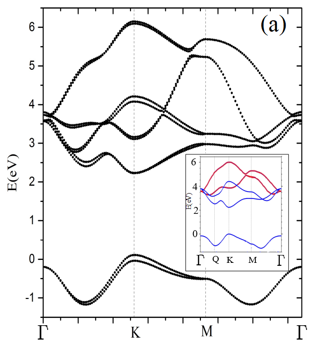
Since the excitonic physics is essential to describe the optical response of semiconducting TMDs, and in view of the current need for accurate, yet expedite, methods to tackle these properties, we solve the BSE and calculate the optical conductivity using an orthogonal SK TB Hamiltonian parameterized to describe the MoS2 band structure. The atomic orbital basis comprises the three valence orbitals in each S plus the five orbitals in each Mo within the trigonal unit cell, giving a total of 11 atomic orbitals. The construction of the Hamiltonian and optimization of its SK parameters has been presented in detail elsewhere Ridolfi et al. (2015). In brief, its main characteristics are: (i) only fitting parameters, (ii) the correct band gap of eV at the point, (iii) the spin splitting of the VB at the point by meV, (iv) the effective masses and positions of the conduction and valence bands at , and at the so-called point. The TB parameters for the SO coupling have been chosen to match with the experimental energy difference between A and B peaks Miwa et al. (2015). The associated band structure is reproduced in Fig. 1(a), reflecting the insulating ground state of a pristine monolayer. The Bloch states, , derived from this Hamiltonian are taken as a good approximation to the eigenstates of the crystal Hamiltonian,
| (1) |
where
| (2) |
The lattice vector runs over all unit cells of the crystal, is the band index, denotes the orbitals, and corresponds to the position in the unit cell of the atoms at which the orbitals are centered. Both the band and orbital indices run over the same interval , where (, with spin) is the dimension of the orbital basis considered in the SK Hamiltonian. These Bloch states are used to set up the BSE in the Tamm-Dancoff approximation (TDA) by introducing a basis of two-particle excitations of the Fermi sea, ,
| (3) |
The latter are used to express the exciton states
| (4) |
with energy , where labels the excitonic modes.
Note that these definitions implicitly restrict the exciton momentum to zero; this is sufficient to capture all first order optical processes, as the excitons with zero momentum are the optically bright ones. Hence, we restrict our discussion to this subspace only. Furthermore, we employ the traditional notation “” to designate conduction and valence bands in order to emphasize that we shall be working at zero temperature. It is also instructive to note at this point that, since , and where / is the number of conduction/valence bands, the dimension of the vector space spanned by the basis states in Eq. (3) is , where represents the total number of points sampled in the BZ. The number of bands and the size of the sampling in points is one of the critical limiting factors in calculations of the two-particle spectrum, even within a parameterized TB framework.
Replacing (4) in the Schrödinger equation that includes the many-body Coulomb interaction yields the reduced eigenproblem Grosso and Parravicini (2014); Trolle et al. (2014); Wu et al. (2015)
| (5) |
Here, is the energy difference between the and bands at , is the total area of the crystal ( with Å the lattice constant) and represents the matrix element of the many-body Coulomb potential, , between two particle-hole excitations. In the TDA, there are two contributions to this matrix element: a direct and an exchange term 222For the derivation of the BSE in details on the computation of see, for instance, Chapters VII.1. and IV.4-5 of LABEL:~Grosso and Parravicini, 2014.. As pointed out earlier Wu et al. (2015), in an orthogonal basis and in our approximation where the Coulomb interaction is independent of the orbital character of the states involved, the exchange term does not contribute for zero-momentum excitons. As a result, only the direct Coulomb matrix element remains, which can be expressed simply as Trolle et al. (2014); Wu et al. (2015)
| (6) |
where is the Fourier transform of the screened Coulomb potential Rohlfing and Louie (2000). The orthogonality assumed in defining our SK basis Ridolfi et al. (2015) allows one to express the overlap integrals in terms of the expansion coefficients of the Bloch states (2) as
| (7) |
Since the are obtained from the numerical eigenvectors of the Bloch Hamiltonian (2), it is important to ensure a consistent choice of phase because the are not gauge-invariant quantities. We chose to require the sum of the basis-set coefficients of the wave function to be real, as suggested in LABEL:~Rohlfing and Louie, 2000.
III.2 Screened Coulomb interaction
An accurate approximation to describe the screened Coulomb interaction in Eq. (6) is essential for a realistic description of the excitonic spectrum Rohlfing and Louie (2000). Early attempts to theoretically describe the exciton series in MoS2 and related 2D materials provide a good example of this stringent requirement, since, by simplistically using the bare Coulomb form of the potential, one fails to capture the non-Rydberg level structure observed experimentally Chernikov et al. (2014); Trushin et al. (2017); Srivastava and Imamoğlu (2015). The distinct series of bound exciton levels in MoS2 is due to both its pseudospin degree of freedom Trushin et al. (2017) and the modified electrostatic interaction in strictly 2D electronic systems which, in Fourier space, acquires the form Chernikov et al. (2014); Rodin et al. (2014)
| (8) |
where defines the 2D polarizability of the electronic system Cudazzo et al. (2011); Chernikov et al. (2014); Rodin et al. (2014) and captures the static, uniform screening due to the top and bottom media surrounding the MoS2 monolayer Zhang et al. (2014a). We assume a MoS2 monolayer of effective thickness and effective dielectric constant sandwiched between materials with dielectric constants and . The environment dielectric constant is thus . The potential (8) has precisely the form derived by Keldysh for a thin metallic film, in which case the parameter enters as the film thickness Keldysh (1979). The explicit -dependence in the dielectric function due to many-body interactions qualitatively modifies Coulomb’s law in real space which becomes
| (9) |
where and are Struve and Bessel functions, respectively. The parameter defines a crossover length scale separating the long-range decay from the short-range domain characterized by a singularity as Cudazzo et al. (2011). Ab-initio studies have confirmed that the Keldysh interaction accurately describes the screened potential in MoS2 Berkelbach et al. (2013); Latini et al. (2015). Thus, we employ in Eq. (6) to solve the BSE.
Only the parameters and remain now to fully specify the content of Eq. (5). They have been reported with a large variation among different authors in the recent literature Zhang et al. (2014a); Wu et al. (2015); San-Jose et al. (2016); Berkelbach et al. (2013). Ab-initio calculations of the 2D polarizability find Å in vacuum Berkelbach et al. (2013). However, it is known that the precise energy placement of the exciton level series is sensitive to the details of the dielectric environment surrounding the monolayer sample Wu et al. (2015); Raja et al. (2017); Chaves et al. (2017); Wang et al. (2017b). Prior estimates for the monolayer in the dielectric environment of an air/substrate interface report values spanning a relatively wide interval, namely, ÅZhang et al. (2014a); Wu et al. (2015); San-Jose et al. (2016); Berkelbach et al. (2013). Since we will be referring to the measurements by Li and collaborators Li et al. (2014) as our reference for the experimental optical conductivity, the environment’s dielectric constant is , as appropriate for the air/silica interface (, ). In the absence of present ab-initio calculations of the corrections to the polarizability due to the effect of a silica substrate, we follow the estimates put forward in Refs. Zhang et al., 2014a; Wu et al., 2015, which are based on the Keldysh-type finite thickness () model:
| (10) |
In this expression, stands for an effective dielectric constant of MoS2. The best agreement with the measured exciton binding energies is obtained with Zhang et al. (2014a) Å and (the latter matches well the results from first principles calculations of the dielectric constant of bulk MoS2 Berkelbach et al. (2013)), resulting in Å333 The expression is sometimes reported as the limit of Eq. (10) when . .
Having thus specified all its contributions, and even though numerically more efficient methods have been proposed recently Trolle et al. (2014), we solved the BSE by full diagonalization of the eigenvalue problem in Eq. (5). In view of the ranges of energy covered in current experiments, we restricted our base states in Eq. (3) to include excitations between valence bands ( since spin is explicitly included) and conduction bands.
Note that, when considering effective models in the (Dirac) approximation it is important to additionally include the pseudospin degree of freedom in the treatment of the effective Schrödinger equation to properly describe the spectrum Trushin et al. (2017).
III.3 Optical response
As the point group determines that all rank 2 tensors are in-plane isotropic, in a MoS2 monolayer it is sufficient to consider the diagonal component of the optical conductivity which is given in linear response by (dipole approximation, ) Trolle et al. (2014); Hipolito (2016)
| (11) |
Using Eq. (4) to express we write the total momentum operator matrix element as
| (12) |
Expanding the many-body momentum operator in the usual way, , one has
| (13) |
where corresponds to the Fermi-Dirac occupation number of an electron at the state . At zero temperature and noting that we are interested in the case where , we write
| (14) |
Hence, inserting here the expression for Bloch states given in Eq. (2), the optical conductivity (11) becomes
| (15) |
This form makes explicit that the oscillator strength associated with each particle-hole excitation involves contributions that depend both on the solution of the BSE (through the eigenvector components ) and on the effective Hamiltonian in the crystal momentum representation (through the components ).
The response in the non-interacting approximation (single-particle) is readily recovered by noting that, in the absence of particle-hole interaction, the BSE, Eq. (5), is diagonal. In this limit, , , and Eq. (15) simplifies to
| (16) |
IV Results
IV.1 Convergence of the exciton spectrum
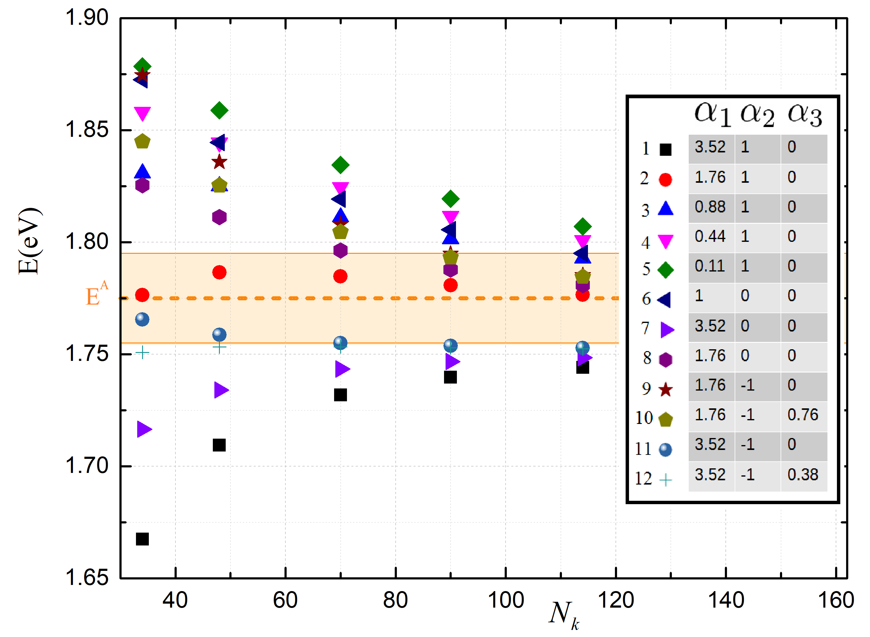
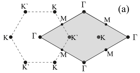
We solve the eigenproblem in Eq. (5) using a uniform sampling of points along the directions defined by the reciprocal lattice vectors , . We place the point at the origin, leaving and at the center of our BZ sampling domain [see Fig. 5(a) below]. Since the Coulomb interaction is not periodic in the reciprocal space and our approach does not include local field terms (i.e., Fourier components beyond the first BZ), the selection of the sampling domain can have an impact on the energies of the bound excitonic levels, especially when these arise from transitions at points near BZ boundaries. More specifically, in the summation performed in Eq. (5), formally runs over the whole reciprocal space, which can be expressed by defining , with spanning the first BZ and the reciprocal lattice. When the excitonic states have wave functions strongly localized near the edges of the BZ, one must include terms, otherwise one misses important contributions from Coulomb matrix elements between states closely spaced, but in adjacent Brillouin zones. Since the wave functions relevant to our problem are localized in regions around the points in the BZ (to be discussed below, see Fig. 5), our choice of the -domain gives converged results for the excitonic spectrum in agreement with the experiment reported in LABEL:~Li et al., 2014 by keeping only (i.e. by considering all wave vectors and matrix elements within the first BZ). Being able to work with this truncation of the Coulomb matrix elements without affecting the convergence of the spectrum provides an additional improvement in the numerical efficiency of the calculation.
Note, however, that any discrete approach requires the regularization of the -diagonal matrix elements due to the integrable singularity that arises from the long range tail of the screened potential [cf. Eq. (8)]. As their contributions to Eq. (5) become regular in the thermodynamic limit , this regularization is well posed in the sense that the specific way it is performed has no influence on the calculated observables in that limit. However, we find that the regularization strategy significantly impacts the rate of convergence of the spectrum with , to the extent that one can gain an order of magnitude reduction in the dimension of the Bethe-Salpeter matrix for a given convergence target. This is a point of high practical significance because, in an effective SK description such as ours, the number of bands is, by construction, the minimal a priori required set. The BZ sampling thus becomes the limiting factor determining the size and tractability of the numerical problem for a given target precision of the calculated spectrum. Since the singular matrix elements are integrated over the -space, the most straightforward regularization consists in replacing by its average value over a small enclosing domain , namely,
| (17) |
Here, and the constants depend on the geometry of the averaging domain and the truncation level of the expansion (17).
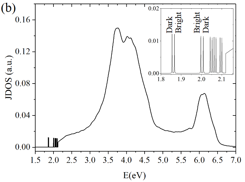
Fig. 2 illustrates the different convergence rate of the lowest exciton level () as a function of the sampling dimension. For demonstration purposes, these data were obtained by solving Eq. (5) with only the two bands of each spin nearest to the bandgap (i.e., ). The asymptotic value is clearly approached much faster for certain choices of the regularization scheme. In particular, one sees that neglecting the leading higher order terms in the expansion (17) by having , (parameter set #, see label in Fig. 2) provides a particularly slow convergence444 Having , in Eq. (17) corresponds to leaving the factor in the potential (8) outside of the average integral. . This is not unexpected because , which is precisely of the same magnitude as those values of that are within practical numerical reach555 Recall that if , the full diagonalization of the BSE Hamiltonian requires handling a matrix of dimension . For us, with and , that amounts to . . On the other hand, the particular parameter sets # and # (see labels in Fig. 2) provide much faster convergence to the asymptotic value eV within a eV precision666 In particular, # consists of choosing at the center of a square integration domain of side and # in placing at the corner of the same integration square. . This translates into a binding energy eV since the single-particle gap in our SK band structure parametrization is eV Ridolfi et al. (2015) (this value corresponds to the first dark exciton, while the first bright one has eV and binding energy eV). Henceforth, all our calculations will be presented according to the regularization scheme #. We have verified that it works efficiently for the whole spectrum.
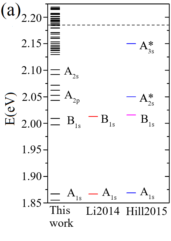
Fig. 3(a) shows a direct comparison between our BSE-derived eigenvalues and experimental spectra measured for MoS2 in silica in the range of the single-particle gap Li et al. (2014); Hill et al. (2015). We find that, except for a global rigid offset of eV, the spectrum obtained with our model parameters reproduces extremely well the bound exciton series. In particular, it captures with accuracy the level spacing of the lowest-lying states which are those most sensitive to the modified screened potential (9) at short distances and, hence, those that most clearly deviate from a hydrogen-like spectrum Srivastava and Imamoğlu (2015); Chernikov et al. (2014); Trushin et al. (2017). This spectrum also captures the fact that the ground excitonic state is dark, as recently established experimentally Molas et al. (2017). We obtain a bright-dark splitting of meV for the lowest excitonic states. This value is due to the 6 meV separation of the conduction bands due to spin-orbit coupling plus differences in effective masses. Our results agree with other theoretical calculations that find meV Echeverry et al. (2016); Baranowski et al. (2017); Malic et al. (2018) depending on the kind of ab-initio approach. So far, the only direct experimental investigation of the bright-dark splitting in MoS2 Molas et al. (2017) finds meV. This value is unexpectedly large in view of the theoretical literature and considering that for TMDs with a larger spin-orbit coupling, like MoSe2 and WSe2, one finds meV Zhang et al. (2017); Molas et al. (2017). These elements indicate that that quantitative aspects of in MoS2 are still under experimental scrutiny.
To allow a direct comparison of the absorption spectrum with the experiments, a rigid blue-shift in the energies by eV has been incorporated in the results shown in Fig. 3. Such a “calibration” is somewhat expected because of the effective parameterizations of both the band structure and the screened Coulomb potential777 Alternatively, the experimental positions of the A and B peaks can be matched by tuning the environment dielectric constants that determine [cf. Eq. (10)] Trolle et al. (2014). (yet, a eV offset is rather small in comparison with similar approaches, where corrections of up to eV were necessary Wu et al. (2015)). This calibration of the energy axis has been also applied in the presentation of all our subsequent results.
The bound series is directly associated with transitions between the topmost valence and bottom conduction bands near the point of the BZ. Each level is 2-fold degenerate on account of the valley degeneracy. When the small energy difference between the two lowest spin-polarized conduction bands at / is ignored, there is an additional 2-fold degeneracy. In our calculations, that small energy difference is explicitly finite [cf. Fig. 1(b)] which explains the existence of two closely spaced levels labeled, for example, A1s, in Fig. 3(a). Nevertheless, one should keep in mind that only half of these excitons are optically bright due to the parity selection rule Wu et al. (2015).
In this respect, it is worth to point out that the difference in the excitation energies of the lowest bound A and B excitons does not follow exactly the spin-orbit spitting of the bands. This is significant because many theoretical TB parameterizations in the literature have identified directly with the SO coupling parameter and, equivalently, this exciton splitting is frequently used as a direct experimental measure of the spin-orbit splitting in the single-particle band structure, which is not strictly correct. For example, we obtain meV while the valence band splitting due to SOC in our chosen TB is 150 meV. The difference can be mainly traced back to the different effective masses of the spin-split valence bands Berghäuser and Malic (2014).
To identify the -point sampling that guarantees convergence of the whole spectrum, we have analyzed the exciton joint density of states (JDOS),
| (18) |
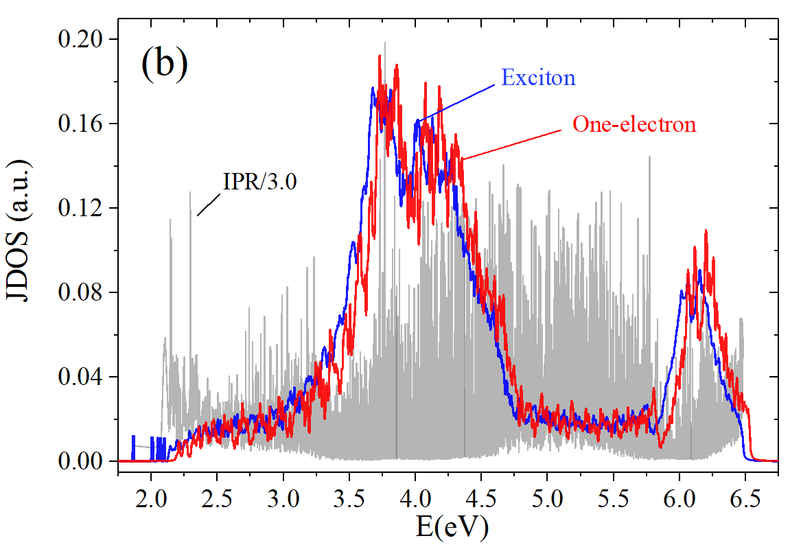
where are the eigenvalues of the BSE. Our calculations show that the JDOS is already reasonably converged for and that the differences for up to are negligible. We take for the results presented in this paper. The converged JDOS calculated with conduction and valence bands is shown in Fig. 3(b) for .
IV.2 Linear optical conductivity
The optical conductivity in linear order is directly obtained from Eqs. (15) and (16) by a diagonalization of the full BSE matrix in the subspace spanned by the 10 bands mentioned above and a suitable sampling of the BZ. The Dirac-delta functions are broadened by replacing them with Lorenzians of full width . The latter qualitatively represents a total decay rate due to several microscopic mechanisms, each of them contributing to with a characteristic energy dependence Qiu et al. (2013). Since the experimental broadening is largely disorder and sample dependent, we take the simple approach of considering as constant and to adjust its value to fit the experimental data (see discussion below).
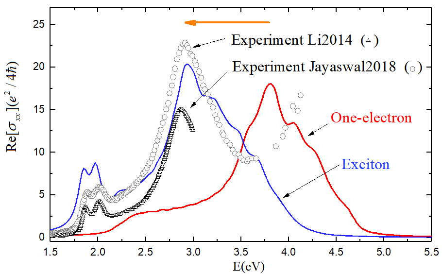
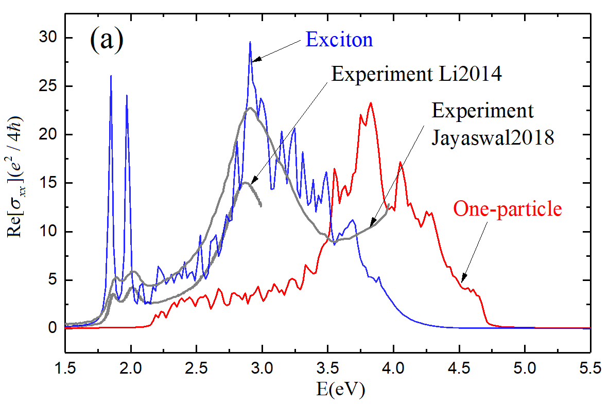
Figure 4 shows the real part of that we obtain for the single-particle and BSE calculations. It is our most significant result. For reference, the plot includes the experimental traces reported recently by Li et al. Li et al. (2014) for exfoliated MoS2 and Jayaswal et al. Jayaswal et al. (2018) for CVD-grown MoS2, both measured on silica at room temperature. Note that the comparison with experimental data is only meaningful up to eV, beyond which excitations involving additional valence bands not included in our present calculation (Fig. 1a) must be taken into account Ridolfi et al. (2015). We put eV in our calculations, which corresponds to the average width of the A and B exciton peaks reported in the experiment of Li et al.. As anticipated, the single-particle results fail to describe the spectral features of the optical response. Even though the discrepancy is most obvious in the region dominated by the bound exciton levels, eV, there is also a remarkable difference in the continuum. In particular, the single-particle spectral weight is generically distributed at energies much above the interaction-corrected values, as highlighted by the horizontal arrow in Figure 4. Therefore, by neglecting the excitonic effects and interpreting the single-particle absorption spectrum literally, one incurs in a severe qualitative and quantitative misrepresentation, not only in the vicinity of the optical gap, but actually over the entire range of energies. Thus, the strong Coulomb interactions in these two-dimensional materials, not only lead to high exciton binding energies, but also largely renormalize the whole spectrum.
Figure 4 shows that our BSE calculation captures rather well the important experimental features of the optical conductivity in MoS2, namely, the position of the A and B peaks, the overall maximum at eV, the energy dependence over the entire experimental range, and the absolute magnitude of the optical conductivity. We stress that we do not adjust or scale the magnitude of , as is frequently done in theoretical work that discusses similar comparisons with experimental data. This overall agreement attests to the validity and accuracy of the SK parameterization of the underlying band structure, and provides strong support to the use of the Keldysh effective screened potential in the BSE calculations (an additional overview of different theoretical and experimental spectra reported in recent literature is given in Fig. 7 of the appendix).
Since corresponds to microscopic processes that depend on the excitation energy, one might expect such dependence to have significant influence in the line shape of the optical conductivity. Yet, our calculation that uses a constant broadening captures the measured energy dependence quite satisfactorily. Surprisingly, ab initio results Qiu et al. (2013); Ramasubramaniam (2012); Klots et al. (2014) are less accurate in describing despite the inclusion of specific energy dependent broadening processes, such as electron-phonon scattering Qiu et al. (2013) [see Fig. 7(b)]. This indicates that the experimental broadening is likely dominated by disorder and justifies a posteriori our choice of an energy-independent to broaden the numerically discrete spectrum in Eq. (15).
Finally, as pointed out in LABEL:~Qiu et al., 2013, convergence studies up to large -sampling meshes are essential to guarantee that one meaningfully “reproduces features in the experimental absorption spectrum above 2 eV”. The comparison presented in Fig. 7 provides a good example of how approaches based on parameterized SK models such as ours can outperform full first-principles solutions of the BSE when it comes to expediency and the need of a large BZ sampling to ensure convergence. It is key, of course, to rely on underlying band structures that accurately describe the quasiparticle renormalization from the outset.
IV.3 Nature of the C excitons
The maximum in at has been attributed to resonant excitons involving transitions near the center of the BZ (the point), the so-called C excitons Qiu et al. (2013). As we discuss below, these excitons are actually not more related to than they are to the point. Hence, it is incorrect to refer to them as “-point excitons”. Turning our attention to the spectral details of the conductivity around , Fig. 4 shows that the energy dependence obtained from the excitonic calculation in the interval eV is nearly identical to that given at the single particle level in the different interval eV. This seems to indicate that, in this energy range, the primary effect of the electronic interaction is to rigidly redshift the one-electron conductivity by about eV, without notable modifications to the line shape (indicated by the horizontal arrow in Fig. 4). That being the case, one could question the attribution of the enhanced spectral weight in this broad region to interaction effects, insofar as (i) the one-electron trace seems to already carry the key aspects of the energy dependence and magnitude of and (ii) the excitonic corrections do not seem to generate any additional spectral feature beyond simply repositioning the curve en bloc to lower energies, as expected from the attractive electron-hole interaction. In other words, it appears as if, for excitation energies belonging to the one-particle continuum, the restructuring of the absorption spectrum caused by interactions amounts to a “scissor”-type correction of the energy spectrum, where an effective “binding energy” of eV brings the one-electron trace (red) to its correct position (blue), but with essentially no changes in oscillator strength. The problem with this, however, is that the value eV is much larger than the binding energy of the A bound excitons ( eV). It turns out that explaining this excitonic redshift on the basis of these one-electron band structure features is questionable and, as we now explain in detail, too simplistic and misleading.
The large spectral weight of the one-electron curve (red in Fig. 4) around its maximum is primarily due to the downward dispersion of the lowest conduction bands along (see Fig. 1): the fact that conduction and valence bands separated by excitation energies eV disperse roughly parallel to each other entails a large enhancement of the one-particle JDOS in this region, naturally explaining the peak in . Equivalently, it can be inferred from Fig. 1 that, in our SK model, the one-electron “optical band structure” is nearly flat along the line. Hence, the one-electron “C peak” is mostly the result of a large one-electron JDOS at eV (see also Fig. 10 in the appendix which explicitly confirms this).
However, the same conclusion does not apply to the results of the excitonic calculation. As we have seen in Fig. 3(b), the excitonic JDOS is peaked, broadly speaking, at eV while the corresponding conductivity peaks at eV. It follows that the enhanced optical response near is, clearly, not the result of a large number of excitonic levels with energies close to . In reality, except for the bound excitonic levels that emerge in the gap, the one-particle and excitonic JDOS do not differ much at energies in the continuum, as we demonstrate in Fig. 10 (appendix). For example, predicting the spectral shape of the optical conductivity solely on the basis of the excitonic spectrum (through the JDOS) would clearly fail for the energies in the continuum. This is the reason why the idea of an effective “binding energy” of eV that rigidly redshifts the one-electron spectrum, as discussed above, is misleading.
We must therefore explicitly consider the oscillator strengths which, according to Eq. (15), are given by
| (19) |
Recalling that represents the probability amplitude of the exciton in reciprocal space, the oscillator strength depends not only on the one-electron dipole matrix elements, but also on the specific texture of each excitonic wave function in space.
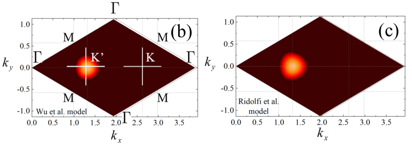
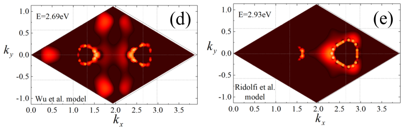
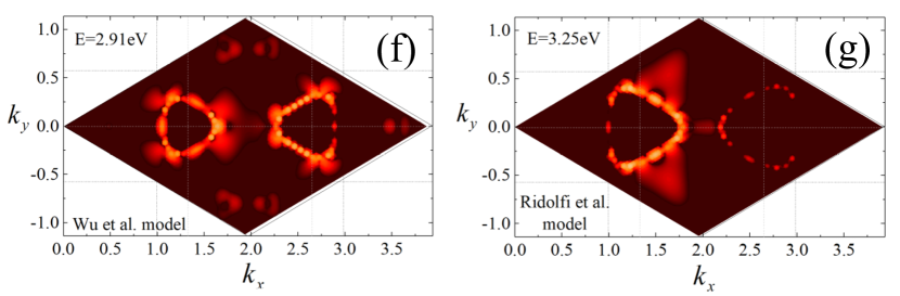
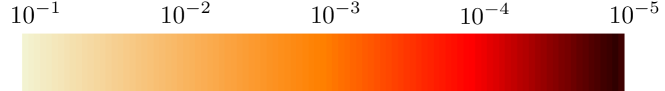
In Fig. 5 we analyze representative excitonic wave functions in reciprocal space associated with the largest optical spectral weights (cf. Fig. 4 and see also Fig. 6 below). As per our earlier remarks regarding the “calibration” of the energies, the values indicated in each panel are shifted by eV (right column) and eV (left column) with respect to the original eigenvalues of the BSE. For reference, Fig. 5(b) and 5(c) show that the wave functions associated with the A and B excitons concentrate at the vicinity of the points 888The results for the B excitons are not shown explicitly, but are similar to those reported in Fig. 5 for the A counterparts., as has been well established by previous calculations. The degree of their localization is directly related to the large binding energies and, in real space, they appear much more localized than typical excitons in semiconductors Wu et al. (2015); Wang et al. (2017a). We recall that, due to the parity selection rule, only half of the excitons related to the two valence and two conduction bands straddling the gap are optically bright. Each of the optically bright excitons is 2-fold degenerate on account of the – valley degeneracy (when the small energy difference between the two lowest spin-polarized conduction bands at / is ignored, these are further degenerate with the other pair of doubly-degenerate dark excitons. In our calculations, that small energy difference is explicitly finite, in correspondence with the spectrum shown in Fig. 3).
The picture is rather different for the C excitons. The wave functions shown in panels (d) to (g) of Fig. 5 correspond to selected states with energies close to . We caution the reader that, unlike the case of bound excitons such as A or B, here we show selected representative wave functions of a “continuum” of states. (We have checked over a window of energies near that the spreading of the wave functions over portions of the BZ similar to those shown here is a robust common feature.) Obviously, the two TB models we use Wu et al. (2015); Ridolfi et al. (2015) render different states. We note, however, the corresponding wave functions show rather large similarities (compare the left and right columns in Fig. 5). Remarkably, there is no pronounced contribution right at the point itself; on the contrary, for our choice of primitive cell, the excitonic wave functions appear distributed on a ring at a finite distance from all the symmetry points, midway between and . This agrees with similar observations based on full ab initio solutions of the BSE in the region of the C excitons which, likewise, associate C excitons with transitions within a similar annular region, but not specifically at or near Qiu et al. (2013); Klots et al. (2014); Molina-Sánchez et al. (2015) (see, for example, Fig. 21 in LABEL:~Molina-Sánchez et al., 2015). Further, the C excitons in Fig. 5 appear as more tightly localized in space than their A counterparts, since the rings are rather thin (keep also in mind that the color scale is logarithmic).
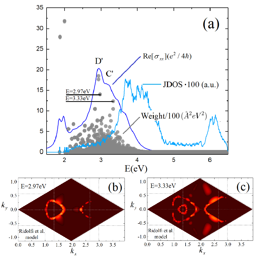
This localization is established at a quantitative level by a computation of the inverse participation ratio associated with each exciton wave function, which we describe in the appendix. The data shown there, in Fig. 10(b), reveal that while the region of the C excitons is characterized by a comparatively small JDOS, the corresponding states are typically more localized than the average 999 At a technical level, it is important to realize that the sharp localization associated with the C excitons requires a fine -point mesh to ensure proper convergence of the absorption spectrum over this large range of energies Qiu et al., 2013. . This ultimately determines the energy dependence of the oscillator strength, which is maximized in the region of energy near , as can be directly seen in Fig. 6 where the quantity (19) is shown for all excitons. Therefore, opposite to the case of a single-particle calculation, the spectral profile of is almost entirely determined by the oscillator strength and not the optical JDOS.
In conclusion, the discussion above indicates that it is misleading to designate these as “-point excitons” and reinforces the perspective that relates them with the properties of the “optical band structure” along the and directions Qiu et al. (2013); Klots et al. (2014). Extending the calculation of the excitonic wavefunctions shown in Fig. 5 to include not only the lowest 2 but all 8 conduction bands in our TB model, we can conclusively assign the two peaks in the oscillator strength at eV and eV (labeled as D’ and C’ in Fig. 6) to the two contributions distinguished in LABEL:~Aleithan et al., 2016. Specifically, with our band structure, they arise from particle-hole excitations between approximately parallel bands eV apart along the and symmetry lines. From this point of view, excitons belonging to the broad C region do have a large binding energy of about eV (). Notably, a comparison between Fig. 5(g) and Fig. 6(c) reveals additional weight in the latter over an inner ring close to . This is contributed by transitions from the valence to the 5th and 6th conduction bands which disperse downwards and nearly parallel to each other eV apart near . This vividly illustrates that the attribution of fine details associated with the whole region of the C excitons is sensitive to the particulars of the underlying bandstructure, and necessitates the inclusion of higher conduction bands.
That C excitons arise from particle-hole excitations midway from the and lines in reciprocal space is consistent with the C peak being more sensitive to the number of layers in thin MoS2 films than the A and B features. In particular, the experimental shift of correlates with the changes in the separation of bands with MoS2 thickness Malard et al. (2013); Dhakal et al. (2014); Klots et al. (2014). These changes in electronic structure are known to be small at the point but large along the whole line, ultimately determining the transition from a direct to indirect gap as a function of thickness Splendiani et al. (2010). The contrast between A/B and C excitons can be understood from the fact that the electronic states at / contain mostly contributions from the orbitals in Mo, while in the regions of that contribute to the C excitons they have a strong character arising from the sulfur atoms Cappelluti et al. (2013); Molina-Sánchez et al. (2015); Ridolfi et al. (2015). As orbitals are spatially more localized and, moreover, lie in the inner of the 3 atomic planes that make each MoS2 monolayer, the A and B exciton states at / are not as perturbed in a stacked multilayer structure or as a result of strain, in comparison with the changes that occur to the C excitons due to their strong sulfur orbital content Molina-Sánchez et al. (2015).
V Summary
We revisited the problem of calculating the excitonic spectrum in the MoS2 monolayer. It has been shown that many-body effects strongly restructure the optical absorption spectrum over an unusually large range of energies in comparison with the single-particle picture. Our approach accounts for the anomalous screening in two dimensions and for the presence of a substrate, both modeled by a suitable effective Keldysh potential. We solve the Bethe-Salpeter equation for the interacting electron-hole excitations by using a Slater-Koster tight-binding model parametrized to fit the calculated first-principles band structure of the material. The optical conductivity that emerges captures with good accuracy both the shape and absolute magnitude of the experimental data.
Our calculation does not consider any temperature-induced change in the band structure nor microscopic broadening mechanisms such as those from the unavoidable phonon excitations. Indeed, by solving a temperature-dependent BSE based on first-principles electron and phonon spectra, Molina-Sanchéz et al. Molina-Sánchez et al. (2016) have shown that the electron-phonon coupling is responsible for most of the 40 meV red-shift observed between zero and room temperature Kioseoglou et al. (2016). In addition to this, for quantitative and qualitative accuracy at the microscopic level, one must consider the impact of the thermal expansion in the band structures and, in the case of excitons, the broadening contributed by radiative recombination. Details of such processes are, however, not in the scope of the present work; in many experimental cases, such microscopic details are overwhelmed by disorder-induced broadening. To compare our results with experiments at room temperature, we blue-shifted the calculated optical response spectrum by 70 meV and introduced a phenomenological broadening, as discussed in Sec. IV.
Seeing that our result captures well the experimental spectrum up to eV, we relied on the predictions of this model to investigate the effects and characteristics of the so-called C excitons. Notably, we explicitly showed in Fig. 5 that they arise from particle-hole excitations in an annular region of the BZ centered at, but at finite radii from, the points (maximal contributions arise from regions between and ).
The interplay between the texture of the excitonic wave functions and the one-electron dipole matrix elements is responsible for the massive transfer of spectral weight seen in the conductivity when compared with results at the one-electron level (Fig. 4). Our results also suggest a cautionary word when it comes to effective mass descriptions of the MoS2 band structure, especially if the aim is to describe the optical excitations in the vicinity of . In this case, a model that captures only the band structure at the point will be certainly insufficient for that.
Throughout our analysis, we presented results obtained using two different tight-binding descriptions of the underlying single-particle band structure. This provides an example of the immediate transferability in this approach to study the optical response of other members of the TMD family. In such a case, one can readily use the same orbital basis for the TB model and the only material-dependent input is the corresponding band structure. The generic workflow is the same as the one we have used above: (i) Obtain an accurate quasiparticle band structure from first principles, (ii) Determine the parameters of the Slater-Koster TB that most faithfully describe such band structure, and (iii) Solve the BSE in the eigenbasis of that TB Hamiltonian.
Our analysis of two different TB parameterizations also affords a perspective over some aspects that are robust in this approach and others that depend on fine details of the parameterization. Overall, the accuracy of our results based on the SK model developed in LABEL:~Ridolfi et al., 2015 vividly supports the use of effective models to expeditiously explore the properties of excitons in 2D materials. This work shows it to be a reliable strategy, provided that the starting Hamiltonian faithfully describes the quasiparticle-corrected band structure. These approaches are orders of magnitude faster in CPU time than complete first-principles solutions of the BSE. Such an advantage facilitates properly addressing the optical response of MoS2 at energies around the C excitons, where a fine sampling of the -space is necessary. We believe that, due to their intrinsic flexibility to model reliably a variety of conditions such as heterostructures, disorder and strain, effective models open the path for a more comprehensive investigation of the optical properties of TMDs where interaction effects play a fundamental role.
Acknowledgements.
We acknowledge fruitful discussions with P. E. Trevisanutto, V. Olevano, T. G. Pedersen, L. Lima, F. Wu, F. Qu, and M. L. Trolle. E. Ridolfi was supported by the Singapore Ministry of Education under grant number MOE2015-T2-2-059. This work was further supported by the Singapore Ministry of Education Academic Research Fund Tier 1 under Grant No. R-144-000-386-114 and the Brazilian funding agencies CNPq, CAPES, and FAPERJ. Numerical computations were carried out at the HPC facilities of the NUS Centre for Advanced 2D Materials.Appendix
V.1 Optical conductivity: compilation of theoretical results
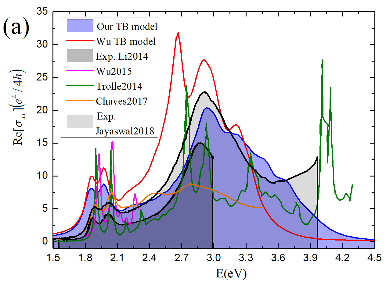
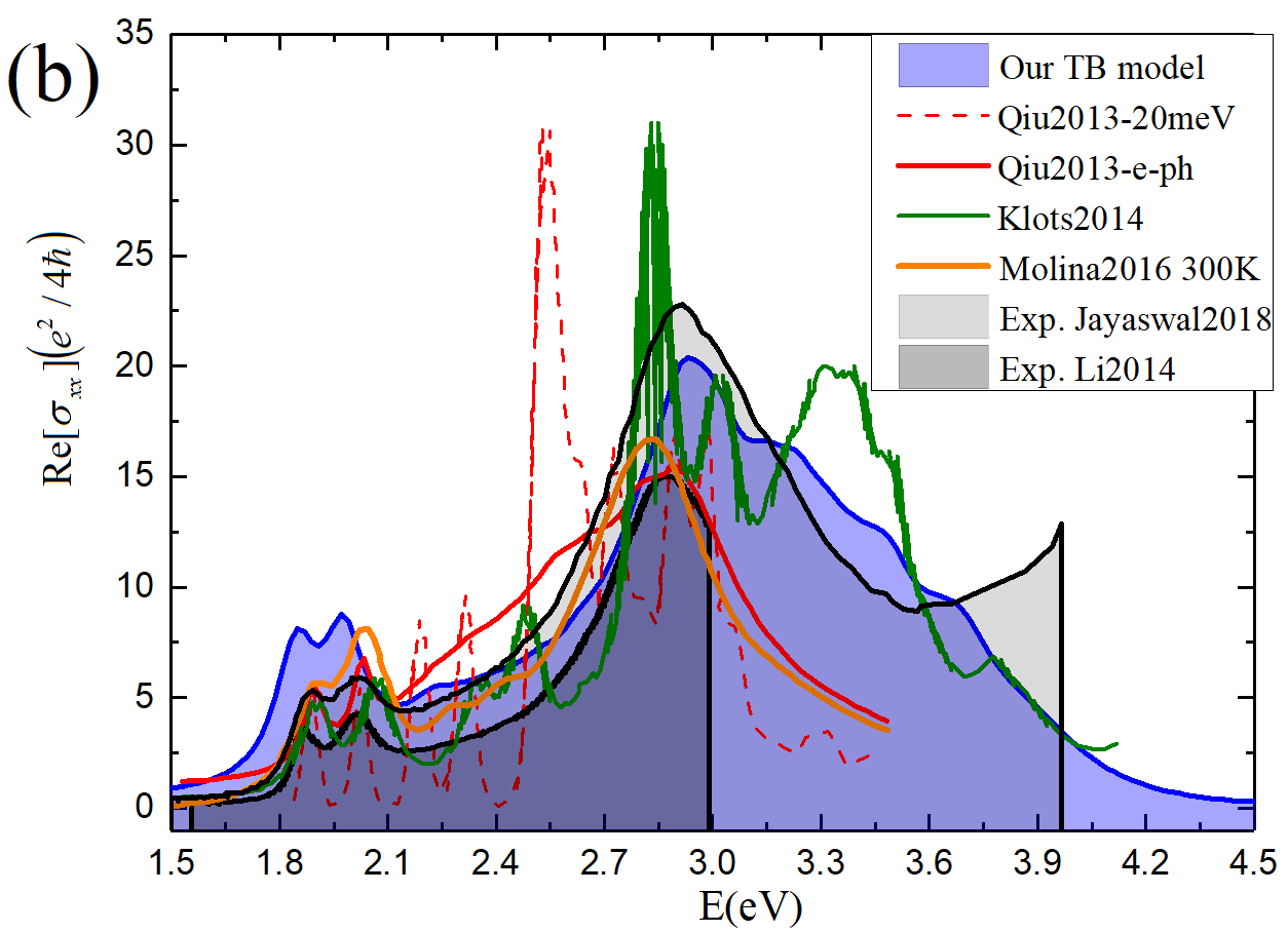
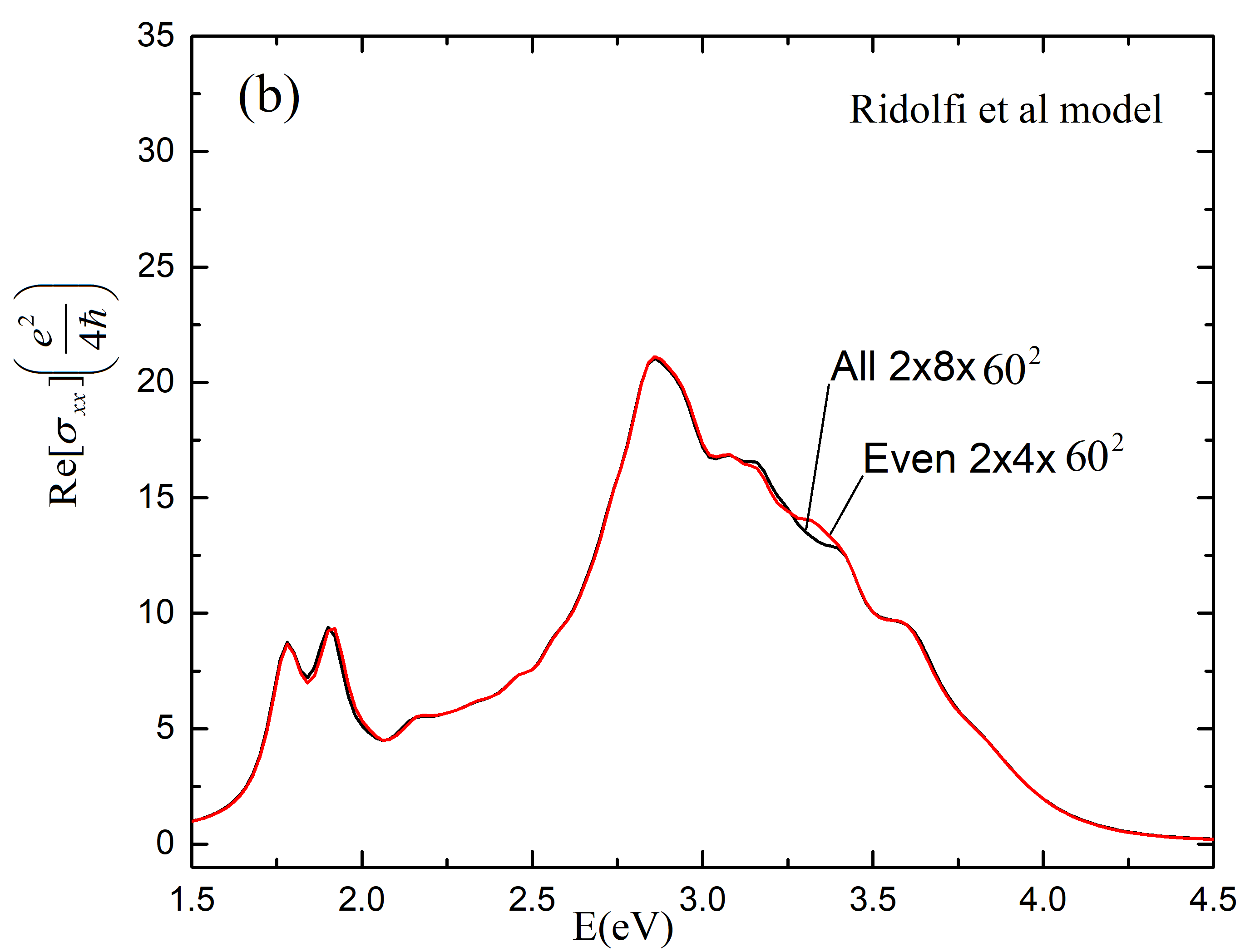
Figure 7 gives an overview of different theoretical results for the optical conductivity in MoS2 found in the literature. Panel (a) compiles TB-based calculations Trolle et al. (2014); Chaves et al. (2017); Wu et al. (2015), while panel (b) compares ab initio results Molina-Sánchez et al. (2016); Qiu et al. (2013); Klots et al. (2014).
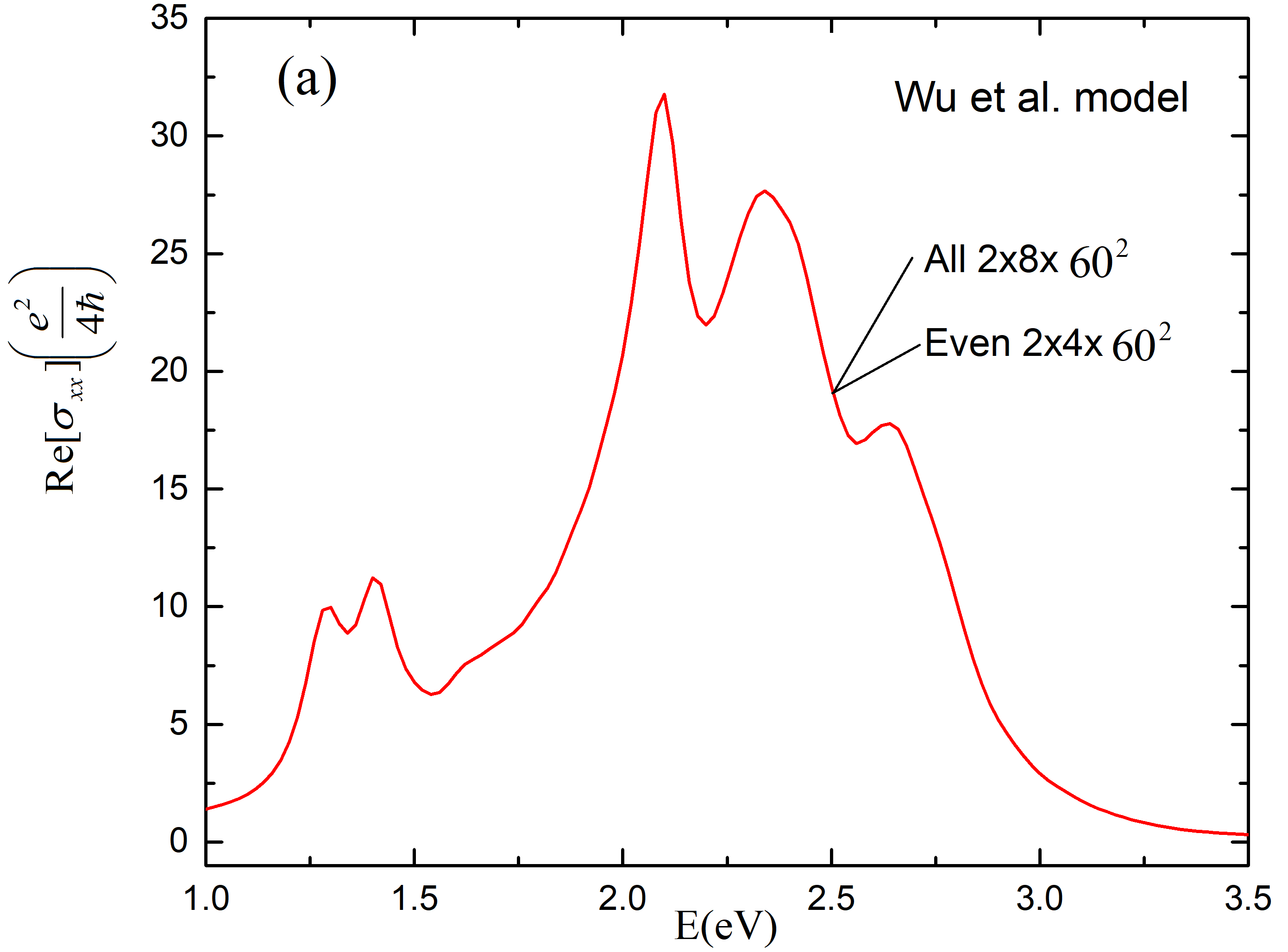
In the case of the TB model, Fig. 7 shows both the given in LABEL:~Wu et al., 2015 as well as the our BSE calculation using Wu and collaborators Wu et al. (2015) TB parameterization over a wider energy range with a suitable broadening adapted to the experimental traces. Figure 7 indicates that the different theoretical approaches describe roughly the same behavior of around the and peaks101010 We stress, however, that some models require rather large rigid shifts in energy and/or vertical scaling in order to make the calculated results agree with the experimental traces as shown in Fig. 7. . In contrast, the energy dependence and spectral weight in the interval eV that covers the region of the excitons are significantly approach dependent. In the particular case of the two TB models that we analyze in detail, these differences can be traced to the larger splitting of the conduction bands near the point in the model of LABEL:~Wu et al., 2015 and the different orbital content of the Bloch states that dominate the dipole matrix elements 111111 For completeness, it is worth noting that the spectral shape in the range of the excitons measured in MoS2 multilayers changes appreciably with layer number, as shown by the experiments reported in LABEL:~Dhakal et al., 2014. .
V.2 Number of conduction bands
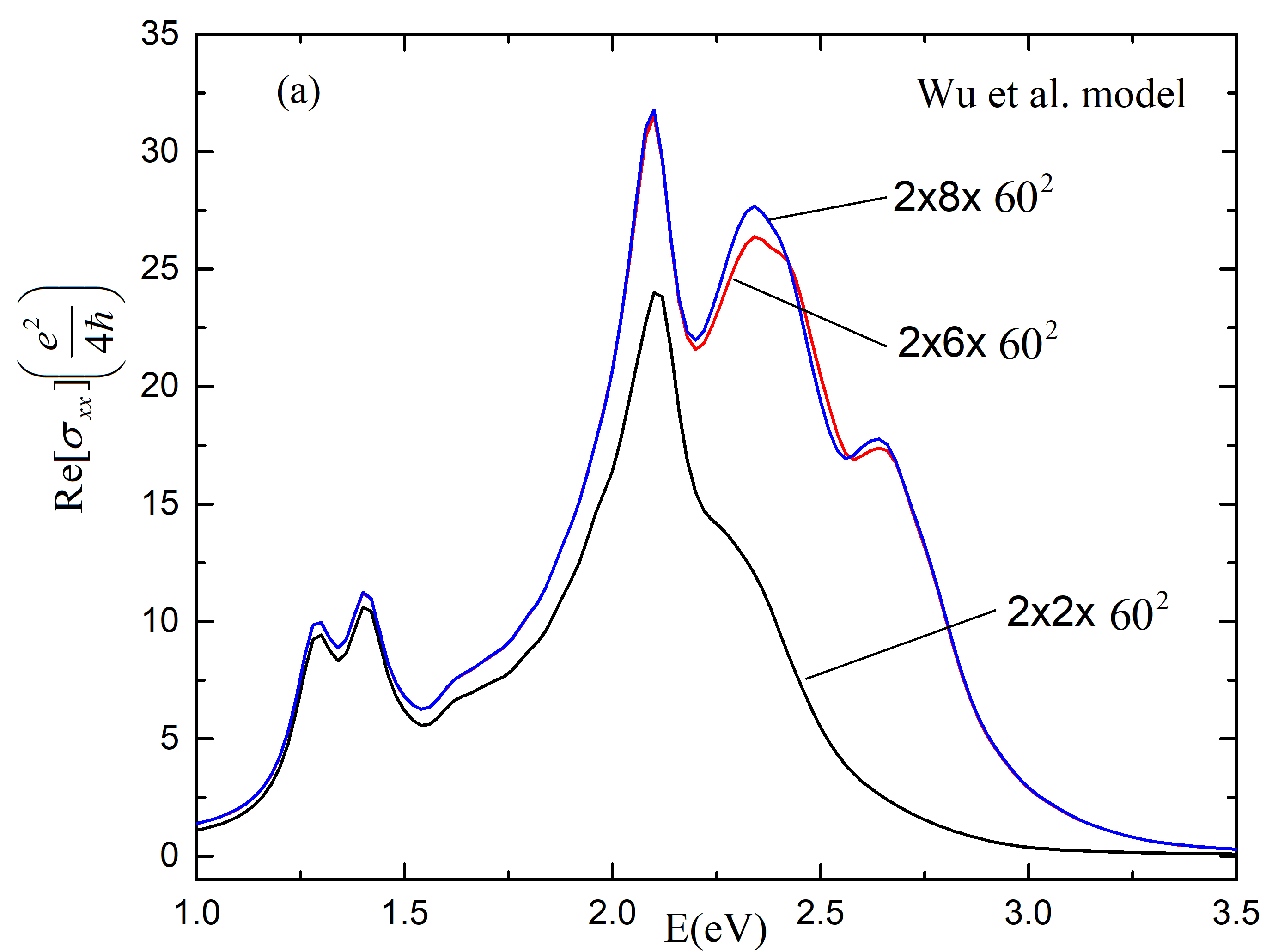
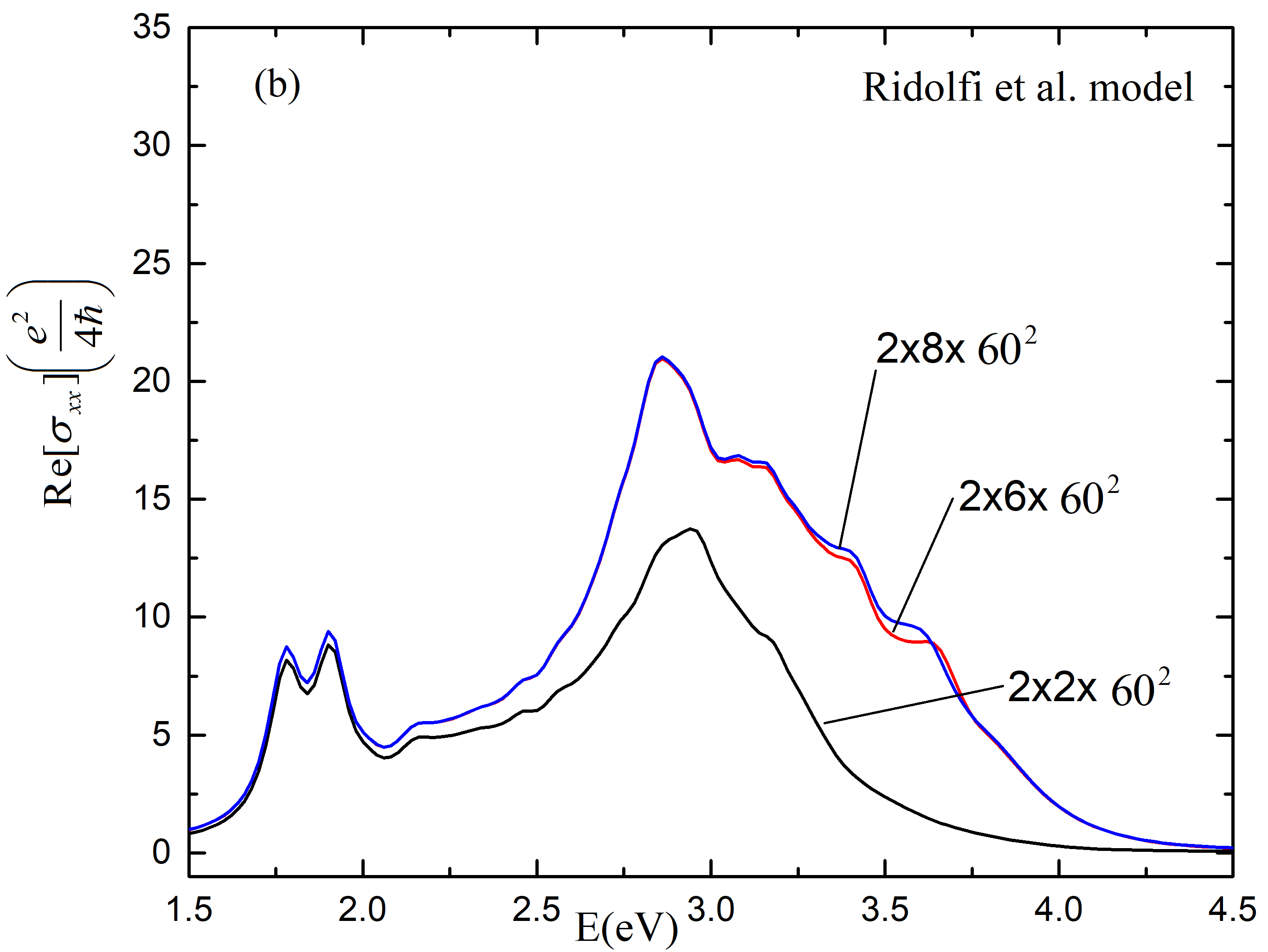
Reference Qiu et al., 2013 reports that the C peak is contributed by 6 nearly degenerate exciton states made from transitions between the highest 2 valence bands and the first three lowest conduction bands (including spin). In Fig. 8 we calculate for , and and verify the necessity of including at least bands. We note that the optical conductivity acquires significant corrections due to the increased number of bands precisely in the energy region of the C excitons for both TB models. In the model of Wu et al. Wu et al. (2015), the C peak is also slightly enhanced when passing from to , while in our TB model the most significant changes occur when passing from to .
V.3 Even and odd bands
The mirror symmetry with respect to the horizontal plane that contains the transition metal ions has important consequences for the band structure of MoS2 monolayers. The TB model that we used to describe the ground-state band structure Ridolfi et al. (2015) predicts one even valence band, two even conduction bands, and two odd parity conduction bands around the Fermi energy [see Fig. 1(a)]. The importance of the odd bands has been unclear Qiu et al. (2013), and we examine this issue next.
Figure 9(a) shows that the odd bands of the TB model of LABEL:~Wu et al., 2015 do not contribute to the optical conductivity. This is expected because this TB model does not include spin-flipping terms: since the dipole coupling is diagonal in spin, the non-zero transition matrix elements must involve initial and final states with the same parity under a reflection with respect to the plane. Our TB model gives a small difference between the all even and odd bands basis caused by the coupling of odd and even bands by the spin-flip terms in the Hamiltonian. We conclude that the increment in the optical conductivity when increasing the number of bands comes mainly from the two upper “even” bands.
V.4 Exciton and one-electron JDOS
When interpreting the origin of the spectral weight shift in the optical conductivity associated with the C excitons, it is useful to analyze how the excitation spectrum itself changes in the presence of the Coulomb interaction. Fig. 10(a) shows the same data for that was presented in Fig. 4, but using a considerably smaller broadening to reveal more clearly the fine spectral structure. In Fig. 10(b) we compare the joint density of states (JDOS) with and without interaction. Apart from the emergence of the bound excitonic states in the gap, we can see that the excitation spectrum largely maintains the JDOS computed at the one-electron level. The interaction causes a global redshift of about eV, which is much smaller than the spectral weight transfer seen in the conductivity. This figure additionally includes the inverse participation ratio (IPR) of all the excitonic levels (20), which quantifies the degree of localization of the respective wave functions in reciprocal space.
V.5 Exciton inverse participation ratio
To have an overall perspective over the degree of localization of each exciton’s wave function, we computed the inverse participation ratio (IPR),
| (20) |
for all the eigenfunctions of the BSE (5). This quantity provides a rough measure of the spread (in reciprocal space) of the wave function belonging to the exciton with energy , being largest for the most localized states and scaling for states uniformly extended over the whole BZ. The result is included in Fig. 10(b). It reveals that while, on the one hand, the region of the C excitons is characterized by a comparatively small JDOS, on the other, states there are typically more localized than the average, as revealed by a number of peaks of the IPR in the interval eV. This simply reflects what has been inferred from the selected wave functions shown in Fig. 5 and, moreover, confirms our earlier statement that C excitons are considerably more localized than bound ones in reciprocal space: . This, of course, is as expected because the latter are true bound states in real space (in relation to this, note that a pure Bloch state has since its wave function is entirely localized at the point in the BZ).
References
- Wang et al. (2012) Q. H. Wang, K. Kalantar-Zadeh, A. Kis, J. N. Coleman, and M. S. Strano, Nat. Nanotechnol. 7, 699 (2012).
- Geim and Grigorieva (2013) A. K. Geim and I. V. Grigorieva, Nature 499, 419 (2013).
- Butler et al. (2013) S. Z. Butler, S. M. Hollen, L. Cao, Y. Cui, J. A. Gupta, H. R. Gutiérrez, T. F. Heinz, S. S. Hong, J. Huang, A. F. Ismach, E. Johnston-Halperin, M. Kuno, V. V. Plashnitsa, R. D. Robinson, R. S. Ruoff, S. Salahuddin, J. Shan, L. Shi, M. G. Spencer, M. Terrones, W. Windl, and J. E. Goldberger, ACS Nano 7, 2898 (2013).
- Choi et al. (2017) W. Choi, N. Choudhary, G. H. Han, J. Park, D. Akinwande, and Y. H. Lee, Materials Today 20, 116 (2017).
- Wang et al. (2017a) G. Wang, A. Chernikov, M. M. Glazov, T. F. Heinz, X. Marie, T. Amand, and B. Urbaszek, arXiv:1707.05863 (2017a).
- Komsa and Krasheninnikov (2012) H.-P. Komsa and A. V. Krasheninnikov, Phys. Rev. B 86, 241201 (2012).
- Berghäuser and Malic (2014) G. Berghäuser and E. Malic, Phys. Rev. B 89, 125309 (2014).
- Molina-Sánchez et al. (2013) A. Molina-Sánchez, D. Sangalli, K. Hummer, A. Marini, and L. Wirtz, Phys. Rev. B 88, 045412 (2013).
- Berkelbach et al. (2013) T. C. Berkelbach, M. S. Hybertsen, and D. R. Reichman, Phys. Rev. B 88, 045318 (2013).
- Qiu et al. (2013) D. Y. Qiu, F. H. da Jornada, and S. G. Louie, Phys. Rev. Lett. 111, 216805 (2013).
- Trolle et al. (2014) M. L. Trolle, G. Seifert, and T. G. Pedersen, Phys. Rev. B 89, 235410 (2014).
- Zhang et al. (2014a) C. Zhang, A. Johnson, C.-L. Hsu, L.-J. Li, and C.-K. Shih, Nano Lett. 14, 2443 (2014a).
- Wu et al. (2015) F. Wu, F. Qu, and A. H. MacDonald, Phys. Rev. B 91, 075310 (2015).
- San-Jose et al. (2016) P. San-Jose, V. Parente, F. Guinea, R. Roldán, and E. Prada, Phys. Rev. X 6, 031046 (2016).
- Chaves et al. (2017) A. J. Chaves, R. M. Ribeiro, T. Frederico, and N. M. R. Peres, 2D Mater. 4, 025086 (2017).
- Trushin et al. (2017) M. Trushin, M. O. Goerbig, and W. Belzig, Journal of Physics: Conference Series 864, 012033 (2017).
- Selig et al. (2016) M. Selig, G. Berghäuser, A. Raja, P. Nagler, C. Sch ller, T. F. Heinz, T. Korn, A. Chernikov, E. Malic, and A. Knorr, Nat. Commun. 7, 13279 (2016).
- Wang et al. (2017b) Z. Wang, Y. Xiao, W. Li, R.-Z. Li, and Z.-Q. Li, arXiv:1701.00559 (2017b).
- Grüning and Attaccalite (2014) M. Grüning and C. Attaccalite, Phys. Rev. B 89, 081102 (2014).
- Glazov et al. (2017) M. M. Glazov, L. E. Golub, G. Wang, X. Marie, T. Amand, and B. Urbaszek, Phys. Rev. B 95, 035311 (2017).
- Rhim et al. (2015) S. H. Rhim, Y. S. Kim, and A. J. Freeman, Appl. Phys. Lett. 107, 241908 (2015).
- Wang and Guo (2015) C.-Y. Wang and G.-Y. Guo, J. Phys. Chem. C 119, 13268 (2015).
- Mak et al. (2010) K. F. Mak, C. Lee, J. Hone, J. Shan, and T. F. Heinz, Phys. Rev. Lett. 105, 136805 (2010).
- Splendiani et al. (2010) A. Splendiani, L. Sun, Y. Zhang, T. Li, J. Kim, C.-Y. Chim, G. Galli, and F. Wang, Nano Lett. 10, 1271 (2010).
- Li et al. (2013) Y. Li, Y. Rao, K. F. Mak, Y. You, S. Wang, C. R. Dean, and T. F. Heinz, Nano Lett. 13, 3329 (2013).
- Zhang et al. (2014b) C. Zhang, H. Wang, W. Chan, C. Manolatou, and F. Rana, Phys. Rev. B 89, 205436 (2014b).
- Li et al. (2014) Y. Li, A. Chernikov, X. Zhang, A. Rigosi, H. M. Hill, A. M. van der Zande, D. A. Chenet, E.-M. Shih, J. Hone, and T. F. Heinz, Phys. Rev. B 90, 205422 (2014).
- Dhakal et al. (2014) K. P. Dhakal, D. L. Duong, J. Lee, H. Nam, M. Kim, M. Kan, Y. H. Lee, and J. Kim, Nanoscale 6, 13028 (2014).
- Miwa et al. (2015) J. A. Miwa, S. Ulstrup, S. G. Sørensen, M. Dendzik, A. G. Čabo, M. Bianchi, J. V. Lauritsen, and P. Hofmann, Phys. Rev. Lett. 114, 046802 (2015).
- Hill et al. (2015) H. M. Hill, A. F. Rigosi, C. Roquelet, A. Chernikov, T. C. Berkelbach, D. R. Reichman, M. S. Hybertsen, L. E. Brus, and T. F. Heinz, Nano Lett. 15, 2992 (2015).
- Klots et al. (2014) A. R. Klots, A. K. M. Newaz, B. Wang, D. Prasai, H. Krzyzanowska, J. Lin, D. Caudel, N. J. Ghimire, J. Yan, B. L. Ivano, K. A. Velizhanin, A. Burger, D. G. Mandru, N. H. Tolk, S. T. Pantelides, and K. I. Bolotin, Sci. Rep. 4, 6608 (2014).
- Rigosi et al. (2016) A. F. Rigosi, H. M. Hill, K. T. Rim, G. W. Flynn, and T. F. Heinz, Phys. Rev. B 94, 075440 (2016).
- Aleithan et al. (2016) S. H. Aleithan, M. Y. Livshits, S. Khadka, J. J. Rack, M. E. Kordesch, and E. Stinaff, Phys. Rev. B 94, 035445 (2016).
- Chiu et al. (2015) M.-H. Chiu, C. Zhang, H.-W. Shiu, C.-P. Chuu, C.-H. Chen, C.-Y. S. Chang, C.-H. Chen, M.-Y. Chou, C.-K. Shih, and L.-J. Li, Nat. Commun. 6, 7666 (2015).
- Kumar et al. (2013) N. Kumar, S. Najmaei, Q. Cui, F. Ceballos, P. M. Ajayan, J. Lou, and H. Zhao, Phys. Rev. B 87, 161403 (2013).
- Clark et al. (2014) D. J. Clark, V. Senthilkumar, C. T. Le, D. L. Weerawarne, B. Shim, J. I. Jang, J. H. Shim, J. Cho, Y. Sim, M.-J. Seong, S. H. Rhim, A. J. Freeman, K.-H. Chung, and Y. S. Kim, Phys. Rev. B 90, 121409 (2014).
- Mishina et al. (2015) E. Mishina, N. Sherstyuk, S. Lavrov, A. Sigov, A. Mitioglu, S. Anghel, and L. Kulyuk, Appl. Phys. Lett. 106, 131901 (2015).
- Trolle et al. (2015) M. L. Trolle, Y.-C. Tsao, K. Pedersen, and T. G. Pedersen, Phys. Rev. B 92, 161409 (2015).
- Säynätjoki et al. (2016) A. Säynätjoki, L. Karvonen, H. Rostami, A. Autere, S. Mehravar, A. Lombardo, R. A. Norwood, T. Hasan, N. Peyghambarian, H. Lipsanen, K. Kieu, A. C. Ferrari, M. Polini, and Z. Sun, Nat. Commun. 8, 893 (2016).
- Woodward et al. (2017) R. I. Woodward, R. T. Murray, C. F. Phelan, R. E. P. de Oliveira, T. H. Runcorn, E. J. R. Kelleher, S. Li, E. C. de Oliveira, G. J. M. Fechine, G. Eda, and C. J. S. de Matos, 2D Mater. 4, 011006 (2017).
- Yin et al. (2014) X. Yin, Z. Ye, D. A. Chenet, Y. Ye, K. O’Brien, J. C. Hone, and X. Zhang, Science 344, 488 (2014).
- Zhang et al. (2015) S. Zhang, N. Dong, N. McEvoy, M. O’Brien, S. Winters, N. C. Berner, C. Yim, Y. Li, X. Zhang, Z. Chen, L. Zhang, G. S. Duesberg, and J. Wang, ACS Nano 9, 7142 (2015).
- Liu et al. (2017) F. Liu, J. Zhou, C. Zhu, and Z. Liu, Adv. Funct. Mater. 27, 1602404 (2017).
- Saito et al. (2016) Y. Saito, T. Nojima, and Y. Iwasa, Supercond. Sci. Technol. 29, 93001 (2016).
- Wang et al. (2015) F. Wang, Z. Wang, Q. Wang, F. Wang, L. Yin, K. Xu, Y. Huang, and J. He, Nanotechnology 26, 292001 (2015).
- Raja et al. (2017) A. Raja, A. Chaves, G. A. Jaeeun Yu, H. M. Hill, A. F. Rigosi, T. C. Berkelbach, P. Nagler, C. Schüller, T. Korn, C. Nuckolls, J. Hone, L. E. Brus, T. F. Heinz, D. R. Reichman, and A. Chernikov, Nat. Commun. 8, 15251 (2017).
- Nakajima et al. (1980) S. Nakajima, Y. Toyozawa, and R. Abe, The physics of elementary excitations (Springer-Verlag, Berlin, New York, 1980).
- Roldán et al. (2017) R. Roldán, L. Chirolli, E. Prada, J. A. Silva-Guillén, P. San-Jose, and F. Guinea, Chem. Soc. Rev. 46, 4387 (2017).
- Ugeda et al. (2014) M. Ugeda, A. Bradley, S.-F. Shi, F. H. da Jornada, Y. Zhang, D. Qiu, W. Ruan, S. Mo, Z. Hussain, Z.-X. Shen, F. Wang, S. Louie, and M. Crommie, Nature Materials 13, 1091 (2014).
- Xiao et al. (2012) D. Xiao, G.-B. Liu, W. Feng, X. Xu, and W. Yao, Phys. Rev. Lett. 108, 196802 (2012).
- Mak et al. (2012) K. F. Mak, K. He, J. Shan, and T. F. Heinz, Nat. Nanotechnol. 7, 494 (2012).
- Zheng et al. (2012) H. Zheng, J. Dai, W. Yao, D. Xiao, and X. Cui, Nature Nano 7, 490 (2012).
- Sallen et al. (2012) G. Sallen, L. Bouet, X. Marie, G. Wang, C. R. Zhu, W. P. Han, Y. Lu, P. H. Tan, T. Amand, B. L. Liu, and B. Urbaszek, Phys. Rev. B 86, 081301 (2012).
- Cao et al. (2012) T. Cao, G. Wang, W. Han, H. Ye, C. Zhu, J. Shi, Q. Niu, P. Tan, E. Wang, B. Liu, and J. Feng, Nat. Commun. 3, 887 (2012).
- Bawden et al. (2016) L. Bawden, S. P. Cooil, F. Mazzola, J. M. Riley, L. J. Collins-McIntyre, V. Sunko, K. W. B. Hunvik, M. Leandersson, C. M. Polley, T. Balasubramanian, T. K. Kim, M. Hoesch, J. W. Wells, G. Balakrishnan, M. S. Bahramy, and P. D. C. King, Nat. Commun. 7, 11711 (2016).
- Zhou et al. (2015) J. Zhou, W. Y. Shan, W. Yao, and D. Xiao, Phys. Rev. Lett. 115, 166803 (2015).
- Srivastava and Imamoğlu (2015) A. Srivastava and A. Imamoğlu, Phys. Rev. Lett. 115, 166802 (2015).
- Rohlfing and Louie (2000) M. Rohlfing and S. G. Louie, Phys. Rev. B 62, 4927 (2000).
- Ridolfi et al. (2015) E. Ridolfi, D. Le, T. S. Rahman, E. R. Mucciolo, and C. H. Lewenkopf, J. Phys.: Condens. Matter 27, 365501 (2015).
- Ramasubramaniam (2012) A. Ramasubramaniam, Phys. Rev. B 86, 115409 (2012).
- Molina-Sánchez et al. (2016) A. Molina-Sánchez, M. Palummo, A. Marini, and L. Wirtz, Phys. Rev. B 93, 155435 (2016).
- Tongay et al. (2012) S. Tongay, J. Zhou, C. Ataca, K. Lo, T. S. Matthews, J. Li, J. C. Grossman, and J. Wu, Nano Lett. 12, 5576 (2012).
- Kioseoglou et al. (2016) G. Kioseoglou, A. Hanbicki, M. Currie, A. Friedman, and B. Jonker., Sci. Rep. 6, 25041 (2016).
- Note (1) For example, Ref. \rev@citealpnumQiu2013 attributes the peak C to transitions near, but not directly at, the point, which require a fine sampling with points, and at least bands in the underlying GW calculation. The authors also use local field effects to include the interaction over different BZs.
- Cudazzo et al. (2011) P. Cudazzo, I. V. Tokatly, and A. Rubio, Phys. Rev. B 84, 085406 (2011).
- Chernikov et al. (2014) A. Chernikov, T. C. Berkelbach, H. M. Hill, A. Rigosi, Y. Li, O. B. Aslan, D. R. Reichman, M. S. Hybertsen, and T. F. Heinz, Phys. Rev. Lett. 113, 076802 (2014).
- Rodin et al. (2014) A. S. Rodin, A. Carvalho, and A. H. Castro Neto, Phys. Rev. B 90, 075429 (2014).
- Keldysh (1979) L. V. Keldysh, JETP Lett. 29, 658 (1979).
- Saigal et al. (2016) N. Saigal, V. Sugunakar, and S. Ghosh, Appl. Phys. Lett. 108, 132105 (2016).
- Salpeter and Bethe (1951) E. E. Salpeter and H. A. Bethe, Phys. Rev. 84, 1232 (1951).
- (71) http://www.bethe-salpeter.org.
- Albrecht et al. (1998) S. Albrecht, L. Reining, R. Del Sole, and G. Onida, Phys. Rev. Lett. 80, 4510 (1998).
- Li et al. (2017) J. Li, M. Holzmann, I. Duchemin, X. Blase, and V. Olevano, Phys. Rev. Lett. 118, 163001 (2017).
- Grosso and Parravicini (2014) G. Grosso and G. P. Parravicini, Solid State Physics (Elsevier Science, Oxford, 2014).
- Note (2) For the derivation of the BSE in details on the computation of see, for instance, Chapters VII.1. and IV.4-5 of Ref. \rev@citealpnumGrosso.
- Latini et al. (2015) S. Latini, T. Olsen, and K. S. Thygesen, Phys. Rev. B 92, 245123 (2015).
- Note (3) The expression is sometimes reported as the limit of Eq. (10) when .
- Hipolito (2016) F. M. Hipolito, On linear and non-linear interactions of light with two dimensional materials, Ph.D. thesis, National University of Singapore (2016).
- Note (4) Having , in Eq. (17) corresponds to leaving the factor in the potential (8) outside of the average integral.
- Note (5) Recall that if , the full diagonalization of the BSE Hamiltonian requires handling a matrix of dimension . For us, with and , that amounts to .
- Note (6) In particular, # consists of choosing at the center of a square integration domain of side and # in placing at the corner of the same integration square.
- Molas et al. (2017) M. R. Molas, C. Faugeras, A. O. Slobodeniuk, K. Nogajewski, M. Bartos, D. M. Basko, and M. Potemski, 2D Mater. 4, 021003 (2017).
- Echeverry et al. (2016) J. P. Echeverry, B. Urbaszek, T. Amand, X. Marie, and I. C. Gerber, Phys. Rev. B 93, 121107(R) (2016).
- Baranowski et al. (2017) M. Baranowski, A. Surrente, D. K. M. M. Ballottin, A. Mitioglu, P. Christianen, Y. Kung, D. Dumcenco, A. Kis, and P. Plochocka, 2D Mater. 4, 025016 (2017).
- Malic et al. (2018) E. Malic, M. Selig, M. Feierabend, S. Brem, D. Christiansen, F. Wendler, A. Knorr, and G. Berghäuser, Phys. Rev. Materials 2, 014002 (2018).
- Zhang et al. (2017) X. Zhang, T. Cao, Z. Lu, Y. Lin, F. Zhang, Y. Wang, Z. Li, J. Hone, J. Robinson, D. Smirnov, S. Louie, and . Tony F. Heinz2, Nat. Nanotechnol. 12, 883–888 (2017).
- Note (7) Alternatively, the experimental positions of the A and B peaks can be matched by tuning the environment dielectric constants that determine [cf. Eq. (10)] Trolle et al. (2014).
- Jayaswal et al. (2018) G. Jayaswal, Z. Dai, X. Zhang, M. Bagnarol, A. Martucci, and M. Merano, Opt. Lett. 43, 703 (2018).
- Note (8) The results for the B excitons are not shown explicitly, but are similar to those reported in Fig. 5 for the A counterparts.
- Molina-Sánchez et al. (2015) A. Molina-Sánchez, K. Hummer, and L. Wirtz, Surf. Sci. Rep. 70, 554 (2015).
- Note (9) At a technical level, it is important to realize that the sharp localization associated with the C excitons requires a fine -point mesh to ensure proper convergence of the absorption spectrum over this large range of energies \rev@citealpnumQiu2013.
- Malard et al. (2013) L. M. Malard, T. V. Alencar, A. P. M. Barboza, K. F. Mak, and A. M. de Paula, Phys. Rev. B 87, 201401 (2013).
- Cappelluti et al. (2013) E. Cappelluti, R. Roldán, J. A. Silva-Guillén, P. Ordejón, and F. Guinea, Phys. Rev. B 88, 75409 (2013).
- Note (10) We stress, however, that some models require rather large rigid shifts in energy and/or vertical scaling in order to make the calculated results agree with the experimental traces as shown in Fig. 7.
- Note (11) For completeness, it is worth noting that the spectral shape in the range of the excitons measured in MoS2 multilayers changes appreciably with layer number, as shown by the experiments reported in Ref. \rev@citealpnumKim2014.