Present address: ]Department of Applied Physics and Quantum-Phase Electronics Center (QPEC), University of Tokyo, Hongo, Tokyo 113-8656, Japan, and RIKEN Center for Emergent Matter Science (CEMS), Wako 351-0198, Japan
Spin-current coherence peak in superconductor/magnet junctions
Abstract
Coherence peak effects in a superconductor induced by a thermal spin current are reported. We measured inverse spin Hall effects induced by spin injection from a ferrimagnetic insulator Y3Fe5O12 into a superconductor NbN using longitudinal spin Seebeck effects. In the vicinity of the superconducting transition temperature of the NbN, a large enhancement of the spin Seebeck voltage is observed, whose sign is opposite to that for the vortex Nernst effect, but is consistent with a calculation for a coherence peak effect in the superconductor NbN.
Superconducting spintronics is an emerging research field which explores new spintronic functions by combining superconducting and magnetic orders SCspintronics1 ; SCspintronics2 ; SCspintronics3 ; SCspintronics4 ; SCspintronics5 . One of the key ingredients in the superconducting spintronics is generation of spin-polarized carriers in superconductors spinpolarizedtransport . In conventional s-wave superconductors, a spin-singlet condensate does not carry spin angular momentum. However, thermally excited quasiparticles (QPs) can carry spin angular momenta even in s-wave superconductors SCspintransport . It was theoretically proposed that spin currents due to the spin-polarized QPs are deflected by spin-orbit scattering to yield a charge imbalance along the Hall direction SCspinHall , which can be detected using the technique of the inverse spin Hall effect (ISHE) spinHalleffect ; inversedspinHall ; spininjectionNbN . A giant ISHE due to the QP spin current was indeed observed recently by electrical spin injection into an s-wave superconductor NbN in a lateral spin valve structure quasiparticlespinHall .
A spin Seebeck effect (SSE) is one of the useful ways to generate spin current in magnetic heterostructures by applying a temperature gradient spinSeebeck . In bilayer systems made up of a ferro- or ferri-magnet (F) and a nonmagnetic metal (N), the SSE enables spin injection from the F layer into the attached N layer through a thermal spin pumping originating in a non-equilibrium spin dynamics thermalspinpumping . Several theories have been proposed for the mechanism of the SSE thermalspinpumping ; linearresponseSSE ; SSEtheory ; SSE1 . Adachi et al. formulated the SSE using the linear-response theory linearresponseSSE ; SSEtheory , where the spin current flowing across the N/F interface reflects spin susceptibilities of both layers and the interface - exchange coupling. The injected spin current into the N layer is converted into charge current by ISHE; the ISHE voltage arises in the direction of , where is the spin current and is the spin-polarization vector of electrons in the N layer. Hence ISHE voltage may reflect the spin dynamics of spin-detection layers in SSE measurements according to the theory linearresponseSSE .
In this study, we have investigated ISHE induced by SSE in a superconductor/ferrimagnet (S/F) bilayer comprising a superconductor NbN and a ferrimagnetic insulator Y3Fe5O12 (YIG). We show that the generated ISHE voltage exhibits an anomalous enhancement just below the superconducting transition. The voltage enhancement can be attributed to a coherence peak effect textsuperconductivity ; according to a theoretical calculation, singularity in the QP density of states at superconducting transition temperature () leads to an enhancement of spin dynamics spinpumpingSC in full-gap superconductors. The coherence peak effects have been studied by measuring nuclear magnetic resonance Hebelslichter and ac conductivity skineffect ; conductivity , but the present results show that ISHE is a useful tool for detection of coherence effects in superconductors.
As a F layer, we chose a (111) YIG slab available commercially. A band gap of YIG is 2.85 eV much larger than 4 meV of superconducting gap of NbN YIGenergygap1 ; YIGenergygap2 ; NbNenergygap . Thanks to this energy difference, a superconducting proximity effect is negligible in our measurements proximitySP . The size of the YIG slab is as follows: the lengths along the , , and directions are mm, mm, and mm, respectively [see the coordinate in Fig. 1(a)]. The surface (-plane) of the YIG slab was mechanically polished, and then a 20-nm-thick NbN film was sputtered on it; here, the thickness is greater than the spin diffusion length of 7 nm reported for a NbN film quasiparticlespinHall . For the sputtering, a pure Nb (5N) target was used in a mixture of argon and nitrogen gases at room temperature NbNreactivesputtering1 ; NbNreactivesputtering2 . The base pressure was better than Pa.
The measurement of the SSE was performed using the longitudinal setup with a superconducting magnet criticalsuppression , where an external magnetic field () up to T was applied along the direction in the film plane [-plane in Fig. 1(a)]. The sample was sandwiched by two aluminum-nitride plates. The temperature difference along the axis was applied using a chip resistance heater [Fig. 1(a)] and measured with a couple of type-E thermocouples. The ISHE voltage which arises in the -direction due to () was measured using a nanovoltmeter at each value. As shown in Fig. 1(a), a 30-nm-thick Cu film was deposited at ends of the NbN film, and ohmic contacts were made on the Cu parts for the measurement of ISHE voltage. To compare the ISHE voltage and the transport properties of the NbN layer under a temperature gradient, 4-wire resistance was measured under the same values. The resistance of the NbN layer was used also as a thermometer to determine the average sample temperature of the NbN layer under .
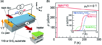
Resistivity, , for the NbN/YIG bilayer measured without applying nor is shown as a function of system temperature, , in Fig. 1(b). The magnitude of is about 270 at K. increases slightly as decreases from 300 K, and suddenly drops around 11 K. The resistivity becomes zero below 10.5 K, signifying superconductivity of the NbN layer. is determined as the temperature where becomes 95 % of the normal state resistivity . In the inset to Fig. 1(b), the dependences of for a NbN/SiO2/YIG trilayer and a NbN/SiO2 bilayer are also shown, where the thickness of the SiO2 layer is nm. The NbN films in NbN/SiO2/YIG and NbN/SiO2 show similar : 11.7 K and 10.6 K, respectively.
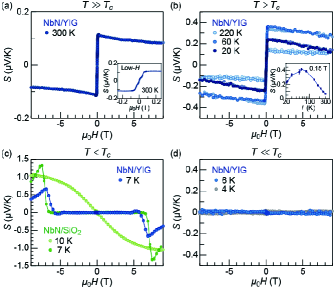
In Fig. 2, we show the experimental results of the SSE measurements, by plotting . Figure 2(a) shows the dependence of measured at 300 K, which is much higher than K. The observed dependence of is antisymmetric with respect to the magnetic field. By increasing from zero, gradually increases reflecting the magnetization in YIG [inset to Fig. 2(a)], but is clearly suppressed by futher increasing ( T). This suppression of is consistent with the typical SSE feature criticalsuppression ; magnon excitations responsible for SSE are suppressed by strong magnetic fields. The sign of is consistent with the spin Hall angle of Nb NbSHC . As decreases in the normal-state regime far above , the magnitude of shows a maximum around K and then decreases with decreasing , as shown in Fig. 2(b).
Figure 2(c) shows the dependence of for the NbN/YIG at 7 K, which is immediately below . The magnitude of is almost zero in the low regime, but suddenly increases at around T. The onset corresponds to a superconducting critical field. A similar behavior is observed in the NbN/SiO2 as shown in Fig. 2(c). In the normal state in the vicinity of the transition, large -induced voltage signals are observed [see Figure 2(c)], which are due to a superconducting vortex flow by thermal gradients. This effect is known as the vortex Nernst effect (VNE), where the vortex flow in the direction of decreasing temperature gives rise to a voltage along the Hall direction vortexNernst1 ; vortexNernst2 ; vortexNernst3 ; vortexNernst4 ; vortexNernst5 . When the direction is reversed, the direction of the magnetic flux of vortices is reversed, and the sign of the voltage due to the VNE is reversed, consistent with the experimental results in Fig. 2(c). Note that the sign of the VNE voltage is opposite to that of the spin Seebeck voltage, as shown in Figs. 2(a), (b), and (c).
As further decreases down to 4 K, which is much lower than , no voltage signal is observed even up to T. At very low temperatures below , the zero-resistivity state persists up to T, which means that vortices are strongly pinned in the NbN layer. Therefore, the voltage due to the VNE disappears in a mixed state at low temperatures SCinTgradient . The voltage due to SSE also disappears owing to the shunting effect due to the zero resistivity nonlocalspininjection . The disappearance of the ISHE voltage in the zero-resistivity state of the NbN is in stark contrast to a previous report on the giant ISHE induced by electrical spin injection into a NbN layer quasiparticlespinHall . In our case, the voltage contact is ohmic, different from the non-ohmic contact in the previous report quasiparticlespinHall , and charge neutrality in the superconductor can be achieved by the cancellation of the QP charge currents and supercurrents textNonEquilibriumSuperconductivity .
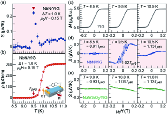
To study SSE signals around in detail, in Fig. 3(a), we show the dependence of around taken at T where is the magnetic parmeability of vacuum. Here, is 1 K, and the sample average temperature shifts from the system temperature by about 1 K. The value is so small that is attributed simply to SSE. The positive sign of in Fig. 3(a) is consistent with the ISHE due to the SSE observed in the normal state above [see Figs. 2(a) and (b)]. Above 10.0 K, is first constant and then decreases with decreasing at 10.2 K. On the other hand, below 9.3 K, is zero. In these two temperature regions, the -dependence of is consistent with that of in NbN.
We found that, surprisingly, in a narrow temperature region 9.3 K10.0 K, the magnitude of is strongly enhanced [Fig. 3(a)]. At the same time, the magnetization of YIG is almost unchanged in the entire temperature range as shown in Fig. 3(c). The enhancement of immediately below cannot be explained by VNE, but is attributable to ISHE induced by SSE for the following reasons. First, the dependence of at 9.5 K almost traces the curve of YIG, as shown in Figs. 3(c) and (d), indicating that the dependence of is relevant to the YIG magnetization. Second, the sign of the enhanced signal is the same as that of the ISHE voltage induced by the SSE, but is opposite to that of the VNE voltage. Third, the enhancement of is not observed in NbN/SiO2/YIG trilayer samples, where the SiO2 layer blocks the transmission of spin currents from YIG to NbN, but VNE is still expected to appear. As shown in Fig. 3(e), on the other hand, negative voltage signals in positive magnetic fields are observed in NbN/SiO2/YIG. is almost linear with respect to in the low- regime, consistent with the VNE observed in the NbN/SiO2 bilayer at similar temperatures shown in Fig. 2(c).
Very recently, spin pumping into superconductors has been theoretically studied spinpumpingSC , and the temperature dependence of the spin pumping efficiency was predicted to exhibit a pronounced coherence peak immediately below YYao . Following the theoretical approach of spin pumping into superconductors textspincurrent , we have calculated the spin current injected into a superconductor due to the SSE in a superconductor/ferrimagnet (S/F) bilayer system. In the presence of between F and S layers, a spin current flows across the interface via SSE. Spin-flip scattering of QPs in the S layer takes place at the interface through the - exchange interaction with localized moments in the F layer, which accompanies a magnon excitation in the F layer. Making use of the BCS-Bogoliubov theory textsuperconductivity and linear response theory for the fluctuation dissipation theorem SSEtheory ; linearresponseSSE , we obtain the spin current flowing across the S/F interface with magnon excitation with the frequency ,
| (1) |
where is the Bose distribution function, and are the effective temperatures of magnons and QPs, respectively, is the temperature-dependent superconducting energy gap, is the QP energy measured from the Fermi energy, Re is the normalized BCS density of states, and is the Fermi distribution function of QPs in the S layer. The factor represents a coherence effect of superconductivity for spin-flip scattering of QPs textsuperconductivity .
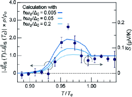
In Fig. 4, we show the numerical calculation of Eq. (1) for several values of . For comparison of the calculation with the enhancement of observed experimentally [Fig. 3(a)], the normalized magnitude of the spin current is multiplied by , and plotted as a function of . Here, we used the values of K and K where is the superconducting gap at for the strongly coupled superconductor NbN textsuperconductivity2 . The temperature scale of is much larger than that of the magnon gap energy of YIG estimated to be K at T, where is the Lande’s factor ( for YIG) and is the Bohr magneton. Hence, we take into account the contribution only from low-frequency magnons in the calculation of Eq. (1). As shown in Fig. 4, the calculated spin-current signal is strongly enhanced just below owing to the superconducting coherence effect, forming a coherence peak in the narrow range below . For lower-frequency magnons (), a larger peak is expected to be produced by the coherence factor multiplied by the densities of states in Eq. (1) textsuperconductivity ; conductivityYBCO .
The experimental values for the SSE signal are calibrated as , where the VNE signal multiplied by the adjusting parameter is subtracted from adjustingparameter . The result for is plotted by filled circles in Fig. 4. As seen in Fig. 4, the temperature range where the enhancement of observed experimentally is reproduced by the calculation; both experimental and theoretical results are largest at 0.96 . The coherence-peak temperature in the calculation is a bit higher than that reported in a microwave conductivity measurement for Nb ( ) Nbcoherencepeak . This may be because, in Fig. 4, the normalized spin current is multiplied by the normalized resistivity which rapidly decreases to zero below . Since measured voltages are zero in the zero-resistivity state, the coherence-peak temperature shifts from 0.9 expected in Eq. (1) to 0.96 in Fig. 4. The magnitude of enhancement is consistent with the theoretical calculation; compared to the normal-state values, the observed signal is enhanced by a factor of at 0.96, and the enhancement in the calculation is for . The small discrepancy in the magnitudes between the experimental and theoretical results could be due to impurity spin-orbit scattering, which may further enhance spin current owing to impurity vertex corrections spinpumpingSC .
In summary, we found that inversed spin Hall voltage induced by spin Seebeck effects in a bilayer film comprising NbN and YIG layers is clearly enhanced in a narrow temperature range immediately below , exhibiting a peak structure. This enhancement appears only in NbN/YIG, not in NbN/SiO2/YIG or NbN/SiO2, where only vortex Nernst voltages whose sign is opposite to the inversed spin Hall voltages were observed. A theoretical calculation of the spin Seebeck effects reveals that a coherence peak effect in the spin Seebeck effects for superconductors in which low-frequency magnons are taken into consideration can be responsible for the anomalous enhancement of the spin Seebeck effects.
Acknowledgment- The authors thank K. Ohnishi and Y. Chen for fruitful discussions. This research was supported by JST ERATO “Spin Quantum Rectification Project” (JPMJER1402), JSPS KAKENHI (No. 17H04806, No. JP16H00977, and No. 16K13827), and MEXT (Innovative Area “Nano Spin Conversion Science” (No. 26103005)). T.K. and J.L. are supported by JSPS through a research fellowship for young scientists (No. JP15J08026 for T.K. and No. JP16J03699 for J.L.). M.U. is supported by GP-Spin at Tohoku University.
References
- (1) J. Linder and J. W. A. Robinson, Nat. Phys. 11, 307-315 (2015).
- (2) D. Beckmann, J. Phys. Cond. Mat. 28, 163001 (2016).
- (3) I. uti, J. Fabian, and S. Das Sarma, Rev. Mod. Phys. 76, 323 (2004).
- (4) A. I. Buzdin, Rev. Mod. Phys. 77, 935 (2005).
- (5) B. M. Andersen, Y. S. Barash, S. Graser, and P. J. Hirschfeld, Phys. Rev. B 77, 054501 (2008).
- (6) R. Meservey and P. M. Tedrow, Phys. Rep. 238, 173 (1994).
- (7) T. Yamashita, S. Takahashi, H. Imamura, and S. Maekawa, Phys. Rev. B 65, 172509 (2002).
- (8) S. Takahashi and S. Maekawa, Phys. Rev. Lett. 88, 116601 (2002).
- (9) A. Hoffman, IEEE Trans. Magn. 49, 5172 (2013).
- (10) E. Saitoh, M Ueda, H. Miyajima, and G. Tatara, Appl. Phys. Lett. 88, 182509 (2006).
- (11) T. Wakamura, N. Hasegawa, K. Ohnishi, Y. Niimi, and Y. Otani, Phys. Rev. Lett. 112, 036602 (2014).
- (12) T. Wakamura, H. Akaike, Y. Omori, Y. Niimi, S. Takahashi, A. Fujimaki, S. Maekawa, and Y. Otani, Nat. Mater. 14, 675 (2015).
- (13) K. Uchida, H. Adachi, T. Kikkawa, A. Kirihara, M. Ishida, S. Yorozu, S. Maekawa, and E. Saitoh, Proc. IEEE 104, 1946 (2016).
- (14) J. Xiao, G. E. W. Bauer, K. Uchida, E. Saitoh, and S. Maekawa, Phys. Rev. B 81, 214418 (2010).
- (15) H. Adachi, J. Ohe, S. Takahashi, and S. Maekawa, Phys. Rev. B 83, 094410 (2011).
- (16) H. Adachi, K. Uchida, E. Saitoh, and S. Maekawa, Rep. Prog. Phys. 76, 036501 (2013).
- (17) L. J. Cornelissen, K. J. H. Peters, G. E. W. Bauer, R. A. Duine, and B. J. van Wees, Phys. Rev. B 94, 014412, (2016).
- (18) M. Tinkham, Introduction to Superconductivity, McGraw-Hill, New York (1975).
- (19) L. C. Hebel et al., Phys. Rev. 113, 1504 (1959).
- (20) D. C. Mattis and J. Bardeen,Phys. Rev. 111, 412 (1958).
- (21) R. Valds Aguilar et al., Phys. Rev. B 82, 180514 (2010).
- (22) R. Metselaar and P. K. Larsen, Solid State Commun., 15, 291 (1974).
- (23) S. Wittekoek, T. J. A. Popma, J. M. Robertson, and P. F. Bongers, Phys. Rev. B, 12, 2777-2788 (1975).
- (24) K. Komemou, T. Yamashita, and Y. Onodera, Phys. Rev. A 28, 335 (1968).
- (25) C. Bell, S. Milikisyants, M. Huber, and J. Aarts, Phys. Rev. Lett. 100, 047002 (2008).
- (26) D. M. Glowacka, D. J. Goldie, S. Withington, H. Muhammad, G. Yassin, arXiv:1401.2276 (2014).
- (27) K. L. Westra et al., J. Vac. Sci. Tech., A8, 1288-1293 (1990).
- (28) T. Kikkawa, K. Uchida, S. Daimon, Z. Qiu, Y. Shiomi, and E. Saitoh, Phys. Rev. B 92, 064413 (2015).
- (29) T. Tanaka, H. Kontani, M. Naito, T. Naito, D. S. Hirashima, K. Yamada, and J. Inoue, Phys. Rev. B 77, 165117 (2008).
- (30) H. Jin, S. R. Boona, Z. Yang, R. C. Myers, and J. P. Heremans, Phys. Rev. B 92, 054436 (2015).
- (31) T. T. M. Palstra, B. Batlogg, L. F. Schneemeyer, and J. V. Waszczak, Phys. Rev. Lett. 64, 3090 (1990).
- (32) H. C. Ri, R. Gross, F. Gollnik, A. Beck, R. P. Huebener, P. Wagner, and H. Adrian, Phys. Rev. B 50, 3312 (1994).
- (33) Z. A. Xu, N. P. Ong, Y. Wang, T. Kakeshita, and S. Uchida, Nature (London) 406, 486 (2000).
- (34) Y. Wang, Z. A. Xu, T. Kakeshita, S. Uchida, S. Ono, Y. Ando, and N. P. Ong, Phys. Rev. B 64, 224519 (2001).
- (35) Y. Wang, N. P. Ong, Z. A. Xu, T. Kakeshita, S. Uchida, D. A. Bonn, R. Liang, and W. N. Hardy, Phys. Rev. Lett. 88, 257003 (2002).
- (36) R. P. Huebener, Supercond. Sci. Technol, 8, 189-198 (1995).
- (37) K. Ohnishi, Y. Ono, T. Nomura, and T. Kimura, Sci. Rep. 4, 6260 (2014).
- (38) D. N. Langenderg and A. Larkin, Non-Equilibrium Superconductivity, North-Holland, Amsterdam (1980) and references therein.
- (39) M. Inoue, M. Ichioka, and H. Adachi, Phys. Rev. B 96, 024414 (2017).
- (40) Y. Yao, Q. Song, Y. Takamura, J. P. Cascales, W. Yuan, Y. Ma, Y. Yun, J. S. Moodera, X. C. Xie, and W. Han, arXiv:1710.10833 (2017).
- (41) S. Maekawa, S. O. Valenzuela, E. Saitoh, and T. Kimura, Spin Current, Oxford University Press (2012).
- (42) J. Bardeen, L.N. Cooper, and J. R. Schrieffer, Phys. Rev. 108, 1175 (1957).
- (43) J. R. Waldram, Superconductivity of Metals and Alloys, Westview Press, Boulder, United States of America (1992).
- (44) F. Gao, G. L. Carr, C. D. Porter, D. B. Tanner, G. P. Williams, C. J. Hirschmugl, B. Dutta, X. D. Wu, and S. Etemad, Phys. Rev. B 54, 700 (1996).
- (45) The value of the adjusting parameter is chosen so that subtracting the pure VNE signal in NbN/SiO2/YIG [Fig. 3(e)] from the signal containing both SSE and VNE in NbN/YIG [Fig. 3(d)] removes the negative VNE contribution at fields T.
- (46) O. Klein, E. J. Nicol, K. Holczer, and G. Grner, Phys. Rev. B 50, 6307 (1994).