Bandstructure and Contact Resistance of Carbon Nanotubes Deformed by the Metal Contact
Abstract
Capillary and van der Waals forces cause nanotubes to deform or even collapse under metal contacts. Using ab-initio bandstructure calculations, we find that these deformations reduce the bandgap by as much as 30%, while fully collapsed nanotubes become metallic. Moreover degeneracy lifting, due to the broken axial symmetry and wavefunctions mismatch between the fully collapsed and the round portions of a CNT, leads to a three times higher contact resistance. The latter we demonstrate by contact resistance calculations within the tight-binding approach.
- PACS numbers
The fascinating mechanical and electrical properties of carbon nanotubes (CNTs) have attracted a lot of attention for a variety of technologies Yakobson et al. (1996); Falvo et al. (1997); Smalley et al. (2003); Franklin et al. (2012); De Volder et al. (2013); Geier et al. (2015); Cao et al. (2015); Qiu et al. (2017). In particular, semiconducting single-wall CNT field-effect transistors have been considered for sub 10 nm technology nodes Cao et al. (2015); Franklin et al. (2012); Qiu et al. (2017); Cao et al. (2017). CNTs provide high-performance channels below 10 nanometers, but the increase in contact resistance with decreasing size dominates the performance of scaled devices as the channel transport becomes ballistic. Only recently low-resistance end-bonded contacts have been demonstrated Cao et al. (2015, 2017), while most commonly used Pd contacts establish side contacts Franklin and Chen (2010). In the latter, an electron has to overcome two barriers: between the metal and the nanotube under the metal and between the nanotube under the metal and the nanotube in the channel. While much efforts have been made to describe the former type of barriers Leonard and Talin (rein), less attention has been drawn to the latter.
Although CNTs have a very large Young’s modulus in the axial direction Yu et al. (2000a), they are rather soft in the radial direction Palaci et al. (2005); Yu et al. (2000b), such that they can be deformed by the influence of van der Waals forces on two adjacent CNTs Ruoff et al. (1993). These deformations are predicted to be much stronger in CNTs partially covered by a metal contact, due to capillary forces Perebeinos and Tersoff (2014). While much efforts in exploring electronic structure in deformed nanotubes have been made Lammert et al. (2000); Giusca et al. (2007); Nishidate and Hasegawa (2008); Nakanishi and Ando (2015) including effects of the external transverse electric field Gunlycke et al. (2006), little is known about how deformations produced by a metal modify the electronic structure and, as a result, the contact resistance.
In this work, we investigate the effect of such deformations on the electronic structure and contact resistance between the metal deformed and the round portions of a nanotube. Geometry relaxations are done using the valence force model Perebeinos and Tersoff (2009, 2014, 2015), electronic structure calculations using Density Functional Theory (DFT) Blaha et al. , and contact resistance calculations within the tight-binding approach Groth et al. (2014). In deformed, but still open semiconducting CNTs, we find bandgap reduction by 10%-30% depending on a tube diameter. The fully collapsed CNTs are found to be metallic. Most importantly, a new mechanism for degeneracy lifting, arising from the interaction among the orbitals on adjacent sidewalls of a collapsed nanotube, leads to qualitatively larger magnitudes of the bands splitting in the fully collapsed CNTs. The band splitting is now several hundreds of meV, such that there is a dramatic impact on transport even at room temperature, unlike in previous work.
To find atomic positions of carbon atoms in CNTs under metal, we employ a semi-atomistic model in which positions of carbon atoms are relaxed in the presence of the metal and substrate, where both are treated by a continuum model, following Ref. Perebeinos and Tersoff (2014). The CNT interatomic interactions are described by the valence force model Perebeinos and Tersoff (2009), in which stiffness against the misalignment of neighboring orbitals is adjusted foo (a) to reproduce the bending stiffness of Perebeinos and Tersoff (2014); Chopra et al. (1995); Tomanek et al. (1993); Blase et al. (1994a). The substrate is planar and rigid, and the metal is isotropic. We choose surface energy as for Pd metal Singh-Miller and Marzari (2009); Tyson and Miller (1977), the most-used contact metal.
Atomic positions are found by minimizing the total energy of the system, described by
| (1) |
where i and j run over carbon atoms in CNT, and , , and are the van der Waals interactions describing CNT self-interaction, the metal-CNT interaction and the substrate-CNT interaction, respectively. These interactions are modelled by the usual 6-12 potential with parameters chosen to reproduce the binding energy (60 meV/carbon atom) and equilibrium spacing 0.34 nm for a flat graphene sheet Low et al. (2012); Zacharia et al. (2004); Spanu et al. (2009). The fifth term is the metal surface energy and the last term is the interaction between the metal and the substrate. For simplicity, we have chosen the same parameters for all van der Waals interactions, such that the wetting angle of the metal on the substrate is 145.
CNT geometry corresponding to the energy minimum in Eq. (1) is used for the electronic structure DFT calculations, employing the PBE/GGA approximation for the exchange-correlation energy Blaha et al. . The vacuum used to separate CNTs is 7 Å and the k-mesh is .
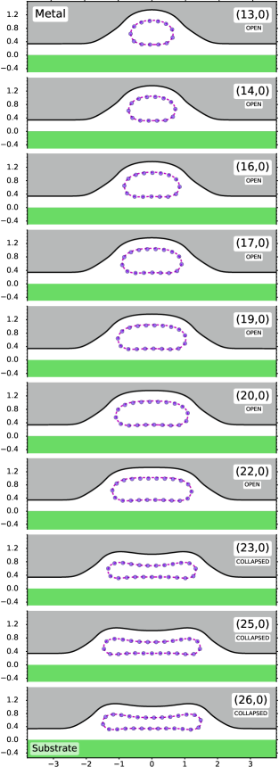
Relaxed geometries of open and collapsed zig-zag CNTs along with the results of a continuum model (Perebeinos and Tersoff, 2014) are shown in Fig. 1. DFT forces normal to the CNT circumference, i.e. along the pi-orbital directions, correspond to a circumference-averaged pressure of about 1-2 GPa, which is consistent with the valence force model calculations in the absence of the metal and the substrate for . The largest open structure CNT we could find is (22,0), although metastable collapsed geometries for (19,0), (20,0), and (22,0) CNTs are found, which is consistent with Ref. Perebeinos and Tersoff (2014, 2015). We find that atomistic and continuum model geometries in Fig. 1 are very similar. Nevertheless, in collapsed CNTs, carbon atoms in the top layer of the collapsed region prefer not to lie on top of carbons in the bottom layer, as shown in Fig. 1. It is energetically more favorable for carbon atoms to slide by half the C-C bondlength in the curvature direction.
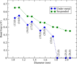
Fig. 2 shows DFT bandgaps in suspended, i.e. round CNTs relaxed in the absence of the substrate and the metal foo (b), and in the metal-deformed CNTs. After deformation, bandgap values are reduced by greater amounts in (3n+1,0) CNTs than in (3n+2,0) CNTs, such that bandgap reductions fall in between 13% for (17,0) and 31% for (22,0) nanotubes. We find all collapsed CNTs to be metallic. We don’t find drastic differences in the electronic structures as we slide atoms along the curvature direction, which is equivalent to rolling the tube along the surface obtained from a continuum model.
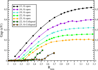
To explore the origins of the electronic structure modifications, we produced deformed CNTs structures within the continuum model by increasing metal surface energy in Eq. (1) and setting van der Waals attraction between the sidewalls to zero, i.e. . The bandgaps gradually reduce with reducing the minimum radius of curvature and become zero at some critical value of Å consistent with Ref. Nishidate and Hasegawa (2008), as shown in Fig. 3. However, when we keep in the total energy minimization, we stabilize collapsed CNTs in which the bandgaps become zero at much larger critical values of Å, as shown in Fig. 3. Moreover, we find that the bandgaps in (22,0) and (25,0) collapsed CNTs are much smaller than those in the open CNTs for the same values of due to the - interactions in the former. Thus we conclude, that - interactions between the orbitals on adjacent sidewalls separated at the van der Waals distance in the collapsed CNTs produce much stronger electronic structure modifications than the curvature induced - interactions.
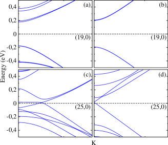
It is expected that changes in the electronic structure caused by the deformations would introduce contact resistance at the interface between the round and the deformed portions of a nanotube. To quantify the magnitude of resistance we solve a scattering problem within a tight-binding formulation Groth et al. (2014). Following Ref. Tománek and Louie (1988), we describe nanotube bandstructure by a four-orbital tight-binding model to account for curvature-induced mixing of and orbitals Blase et al. (1994b). In the case of collapsed CNTs, an additional long-range interaction between carbons belonging to different layers is added Perebeinos et al. (2012). The resulting band structure agrees fairly well with the DFT results, as shown in Fig. 4.
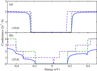
The contact resistances of the round-deformed interfaces in (19,0) and (25,0) nanotubes are shown in Fig. 5a and 5b, correspondingly. As expected, in both cases the conductance is smaller than for a uniform tube, whether round or uniformly deformed, as shown by the dashed curves in Fig. 5. For the interface between the deformed and the round portions of (19,0) nanotube, we see very little scattering due to wavefunction mismatch, such that the contact conductance is around 95% of the ideal conductance, at a typical metal-induced doping level of about 0.1-0.2 electrons per nm. However, a much stronger effect on the resistance is found for the round-collapsed contact interface. Lifting the double degeneracy alone in the fully collapsed (25,0) CNT results in a two times higher contact resistance as compared to the ideal resistance of k. In addition, reflection at the interface causes an additional increase in the resistance.
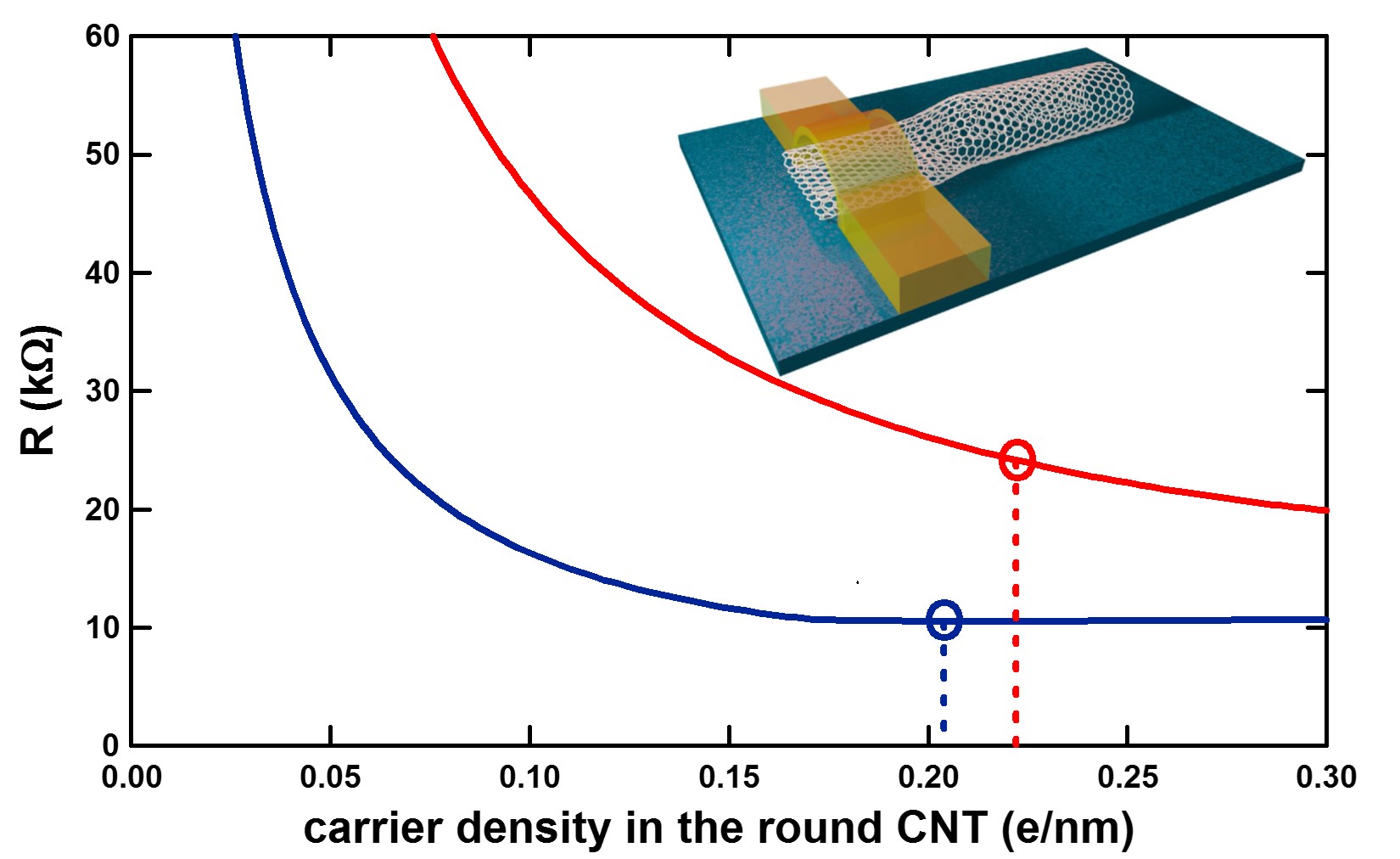
In CNT field-effect transistor, schematic is shown in the inset of Fig. 6, the Fermi level can be modified by an applied gate voltage in the round portion of a CNT. Whereas under the metal, doping is determined by a CNT and metal work function difference, which for Pd contact we assume it to be eV Perebeinos et al. (2013). The metal-CNT capacitance depends on CNT diameter and electrostatic distance Å. We solve self-consistent equations for the charge density in CNT under the metal:
| (2) | |||||
where charge neutrality point is , is the density of states from the DFT calculations, and is the Fermi-Dirac function. Doping determines the number of conduction modes at the Fermi energy and the maximum on-state conductance Guo et al. (2002); Fischetti et al. (2007); Wei et al. (2011) (in the absence of the tunneling current contribution Perebeinos et al. (2013)):
| (3) |
where is the transmission coefficient and the spin degeneracy is included. Using for a round CNT in Eq. (2), the self consistent doping level would be meV, where is the top of the valence band, and an ideal on-state resistance of k follows from Eq. (3), using and K. In the deformed CNT, the self consistent doping level is lower meV due to the smaller bandgap and the ideal on-state resistance is k. By calculating transmission coefficient as a function of doping level in the round portion of the nanotube, which is controlled by the backgate voltage and which we model by introducing a rigid shift of the bandstructure in the round CNT with respect to that in CNT under the metal, we find resistance according to Eq. (3), shown in Fig. 6. We estimate a typical carrier density in the on-state using a wrap around SiO2 gate with dielectric constant and radius 20 nm, and the overdrive backgate voltage of 0.5 V. As shown in Fig. 6, the on-state resistance of k in (19,0) CNT is not very different from the ideal contact resistance from Eq. (3), using .
In the case of fully collapsed (25,0) CNT, the self-consistent Fermi energy of a round CNT under the metal would be meV and the corresponding on-state resistance k. Using of the fully collapsed CNT, self consistent doping is found to be meV and the ideal contact resistance k (should the double degeneracy be preserved). However, for the bandstructures corresponding to the collapsed CNT under the metal but round in the channel, contact resistance calculations suggest a much higher contact resistance, as shown in Fig. 6. This is due to both degeneracy lifting and wavefunction mismatch. For a typical carrier density in the on-state, we find contact resistance of k, three times higher compared to the ideal contact resistance from Eq. (3), using and the doubly degenerate bands.
In conclusion, we identified the major effect of metal-induced nanotube deformations on the electronic structure and the electrical contact resistance at the interface between the deformed and the round portions of a nanotube. While the bandgap reduction in the deformed CNTs increases metal-induced doping of a nanotube, and thus reduces the resistance by increasing the number of the conduction channels, wavefunction mismatch introduces an additional scattering at the contact, hence, partially compensating the effect of doping. Fully collapsed semiconducting nanotubes become metallic with a singly degenerate band at the Fermi level due to the broken axial symmetry. The magnitude of the degeneracy lifting of few hundreds of meV is much larger than room temperature and that in the prior reports. Together with the wavefunction mismatch this leads to a much higher contact resistance as compared to the ideal contact. Our results may shed light to the observations of quantized conductance in large-diameter CNTs Biercuk et al. (2005) with steps quarter as large as usual and stimulate further experimental and theoretical work.
References
- Yakobson et al. (1996) B. I. Yakobson, C. Brabec, and J. Bernholc, Phys. Rev. Lett. 76, 2511 (1996).
- Falvo et al. (1997) M. R. Falvo, G. Clary, R. Taylor, V. Chi, F. P. Brooks, S. Washburn, and R. Superfine, Nature 389, 582 (1997).
- Smalley et al. (2003) R. E. Smalley, M. S. Dresselhaus, G. Dresselhaus, and P. Avouris, Carbon nanotubes: synthesis, structure, properties, and applications, Vol. 80 (Springer Science & Business Media, 2003).
- Franklin et al. (2012) A. D. Franklin, M. Luisier, S.-J. Han, G. Tulevski, C. M. Breslin, L. Gignac, M. S. Lundstrom, and W. Haensch, Nano Lett. 12, 758 (2012).
- De Volder et al. (2013) M. F. De Volder, S. H. Tawfick, R. H. Baughman, and A. J. Hart, Science 339, 535 (2013).
- Geier et al. (2015) M. L. Geier, J. J. McMorrow, W. Xu, J. Zhu, C. H. Kim, T. J. Marks, and M. C. Hersam, Nat. Nanotech. 10, 944 (2015).
- Cao et al. (2015) Q. Cao, S.-J. Han, J. Tersoff, A. D. Franklin, Y. Zhu, Z. Zhang, G. S. Tulevski, J. Tang, and W. Haensch, Science 350, 68 (2015).
- Qiu et al. (2017) C. Qiu, Z. Zhang, M. Xiao, Y. Yang, D. Zhong, and L.-M. Peng, Science 355, 271 (2017).
- Cao et al. (2017) Q. Cao, J. Tersoff, D. B. Farmer, Y. Zhu, and S.-J. Han, Science 356, 1369 (2017).
- Franklin and Chen (2010) A. D. Franklin and Z. Chen, Nat. Nanotech. 5, 858 (2010).
- Leonard and Talin (rein) F. Leonard and A. A. Talin, Nat. Nanotech. 6, 773 (2011) and references therein).
- Yu et al. (2000a) M.-F. Yu, O. Lourie, M. J. Dyer, K. Moloni, T. F. Kelly, and R. S. Ruoff, Science 287, 637 (2000a).
- Palaci et al. (2005) I. Palaci, S. Fedrigo, H. Brune, C. Klinke, M. Chen, and E. Riedo, Phys. Rev. Lett. 94, 175502 (2005).
- Yu et al. (2000b) M.-F. Yu, T. Kowalewski, and R. S. Ruoff, Phys. Rev. Lett. 85, 1456 (2000b).
- Ruoff et al. (1993) R. S. Ruoff, J. Tersoff, D. C. Lorents, S. Subramoney, and B. Chan, Nature 364, 514 (1993).
- Perebeinos and Tersoff (2014) V. Perebeinos and J. Tersoff, Nano Lett. 14, 4376 (2014).
- Lammert et al. (2000) P. E. Lammert, P. Zhang, and V. H. Crespi, Phys. Rev. Lett. 84, 2453 (2000).
- Giusca et al. (2007) C. E. Giusca, Y. Tison, and S. R. P. Silva, Phys. Rev. B 76, 035429 (2007).
- Nishidate and Hasegawa (2008) K. Nishidate and M. Hasegawa, Phys. Rev. B 78, 195403 (2008).
- Nakanishi and Ando (2015) T. Nakanishi and T. Ando, Phys. Rev. B 91, 155420 (2015).
- Gunlycke et al. (2006) D. Gunlycke, C. Lambert, S. Bailey, D. Pettifor, G. Briggs, and J. Jefferson, Europhys. Lett. 73, 759 (2006).
- Perebeinos and Tersoff (2009) V. Perebeinos and J. Tersoff, Phys. Rev. B 79, 241409 (2009).
- Perebeinos and Tersoff (2015) V. Perebeinos and J. Tersoff, Phys. Rev. Lett. 114, 085501 (2015).
- (24) P. Blaha, K. Schwarz, G. Madsen, D. Kvasnicka, and J. Luitz, WIEN2k, An Augmented Plane Wave + Local Orbitals Program for Calculating Crystal Properties (Karlheinz Schwarz, Techn. Universität Wien, Austria).
- Groth et al. (2014) C. W. Groth, M. Wimmer, A. R. Akhmerov, and X. Waintal, NJP 16, 063065 (2014).
- foo (a) Using parameters eV and Å in Ref. Perebeinos and Tersoff (2009) (a).
- Chopra et al. (1995) N. G. Chopra, L. X. Benedict, V. H. Crespi, M. L. Cohen, S. G. Louie, and A. Zettl, Nature 377, 135 (1995).
- Tomanek et al. (1993) D. Tomanek, W. Zhong, and E. Krastev, Phys. Rev. B 48, 15461 (1993).
- Blase et al. (1994a) X. Blase, A. Rubio, S. Louie, and M. Cohen, Euro. Lett. 28, 335 (1994a).
- Singh-Miller and Marzari (2009) N. E. Singh-Miller and N. Marzari, Phys. Rev. B 80, 235407 (2009).
- Tyson and Miller (1977) W. Tyson and W. Miller, Surf. Science 62, 267 (1977).
- Low et al. (2012) T. Low, V. Perebeinos, J. Tersoff, and P. Avouris, Phys. Rev. Lett. 108, 096601 (2012).
- Zacharia et al. (2004) R. Zacharia, H. Ulbricht, and T. Hertel, Phys. Rev. B 69, 155406 (2004).
- Spanu et al. (2009) L. Spanu, S. Sorella, and G. Galli, Phys. Rev. Lett. 103, 196401 (2009).
- Blase et al. (1994b) X. Blase, L. X. Benedict, E. L. Shirley, and S. G. Louie, Phys. Rev. Lett. 72, 1878 (1994b).
- Perebeinos et al. (2012) V. Perebeinos, J. Tersoff, and P. Avouris, Phys. Rev. Lett. 109, 236604 (2012), we introduce a cut off function to supress - interactions within the same plane, i.e. at angles between -orbitals less than .
- (37) We find that forces along the CNT axis direction, can be very large up to 1.1 eV/Å(or 70 GPa) and 2.6 eV/Å(or 160 GPa) in open (19,0) and collapsed (25,0) CNTs, correspondingly. This occurs in a very narrow region of the CNT circumference, where the radius of curvature is very small. This effect is not captured by the valence force model. By relaxing atoms in the z-direction along the nanotube axis, keeping the () coordinates the same in DFT, we confirmed that our main conclusions on the degeneracy lifting are not modified .
- foo (b) Bandstructure modifications caused by the subtrate-induced deformations alone are much smaller than those caused by the metal. (b).
- Tománek and Louie (1988) D. Tománek and S. G. Louie, Phys. Rev. B 37, 8327 (1988).
- Perebeinos et al. (2013) V. Perebeinos, J. Tersoff, and W. Haensch, Phys. Rev. Lett. 111, 236802 (2013).
- Guo et al. (2002) J. Guo, S. Datta, M. Lundstrom, M. Brink, P. McEuen, A. Javey, H. Dai, H. Kim, and M. McIntyre, IEDM Tech. Dig. , 711 (2002).
- Fischetti et al. (2007) M. V. Fischetti, L. Wangt, B. Yut, C. Sachs, P. M. Asbecki, Y. Taurt, and M. Rodwell, Proc. IEEE IEDM , 109 (2007).
- Wei et al. (2011) L. Wei, D. J. Frank, and H.-S. P. Wong, IEEE Trans. on Elect. Dev. 58, 2456 (2011).
- (44) For the transport calculations we use an abrupt junction by setting up the corresponding tight binding matrix elements between the deformed and the round portions of the CNT .
- Biercuk et al. (2005) M. J. Biercuk, N. Mason, J. Martin, A. Yacoby, and C. M. Marcus, Phys. Rev. Lett. 94, 026801 (2005).