Strain induced changes of electronic properties of B–site
ordered double perovskite Sr2CoIrO6 thin films
Abstract
B-site ordered thin films of double perovskite Sr2CoIrO6 were epitaxially grown by a metal-organic aerosol deposition technique on various substrates, actuating different strain states. X-ray diffraction, transmission electron microscopy and polarized far-field Raman spectroscopy confirm the strained epitaxial growth on all used substrates. Polarization dependent Co X-ray absorption spectroscopy reveals a change of the magnetic easy axis of the antiferromagnetically ordered (high-spin) Co3+ sublattice within the strain series. By reversing the applied strain direction from tensile to compressive, the easy axis changes abruptly from in-plane to out-of-plane orientation. The low-temperature magnetoresistance changes its sign respectively and is described by a combination of weak anti-localization and anisotropic magnetoresistance effects.
pacs:
73.50.-h,75.47.-m,75.70.-iI Introduction
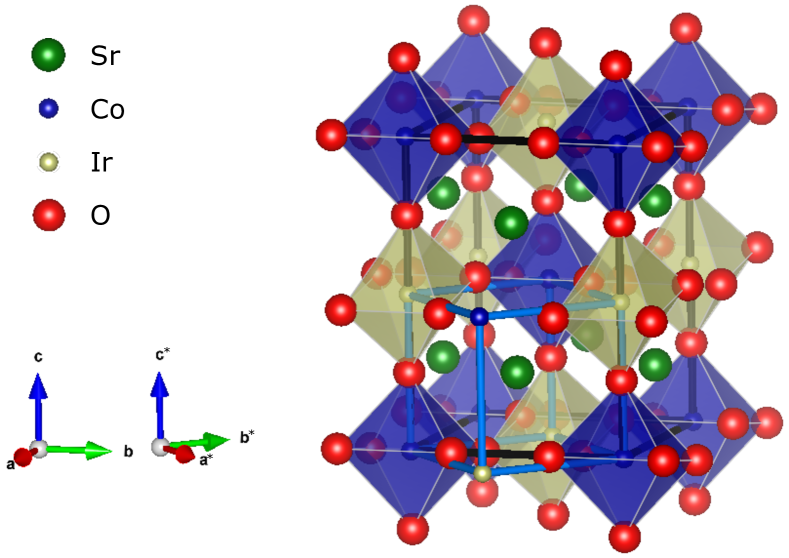
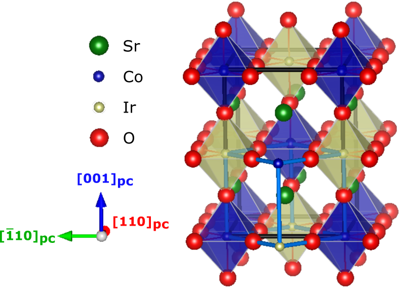
Double perovskites (DPs) A2BB’O6 display interesting electronic and magnetic properties, strongly depending on the degree of the B-site ordering, which as well is determined both by size and valence mismatch of the involved B-site cations RevDP ; Ohtomo ; Anderson . In addition, epitaxial stabilization in thin films could lead to an improvement of B-site ordering as observed for example in the La2FeCrO6 system Chakraverty . The most prominent ordering type of the B-site cations is the rock salt like structure with alternating B and B’ planes along the pseudo cubic [111] direction RevDP , shown in Figure 1 for the title compound of this study. Besides the ferrimagnetic halfmetal Sr2FeMoO6 (Ref. Sr2FeMoO6 ) there are other highly insulating ferromagnetic ordered DPs, like multiferroic La2CoMnO6 (Ref. La2CoMnO6 ) and Ba2CuOsO6 (Ref. Ba2CuOsO6 ), a magnetic insulator recently synthesized und er high-pressure.
Recently, correlated oxides with strong spin orbit (SO) coupling attracted great attention. In particular, the SO coupling in iridates with Ir4+ ( configuration) ions in octahedral coordination results in four occupied and two half-filled states Kim . As was first verified for the layered perovskite Sr2IrO4 (Ref. KimScience ), already a moderate Coulomb repulsion is sufficient to induce a SO Mott insulating state, with magnetic moments. SO coupling is also important for semimetalic iridates PRL114 . As realized by Jackeli and Khalliulin kitaev novel magnetic exchange interactions, in particular the honeycomb Kitaev exchange Kitaev-model , can arise from magnetic moments. This initiated strong interest in two- and three-dimensional honeycomb iridates arXiv .
Iridate DPs offer another novel playground to investigate the electronic and magnetic properties arising from the competition of SO coupling, electronic correlations and structural distortions. This leads, for example, in Sr2CeIrO6 to an insulating state with weak antiferromagnetic (AFM) orbital order Sr2CeIrO6 . Also both La2MgIrO6 and La2ZnIrO6 host SO Mott insulating magnetic states La2XIrO6 . Sr2YIrO6 represents a class of DPs with Ir5+ configuration and evidence of novel magnetism has been reported PRL112 . However, subsequent work PRB95-Sr2YIrO6 , also on the isoelectronic Ba2YIrO6 PRB96-Ba2YIrO6 related these observations to diluted paramagnetic impurities.
Strontium-iridate derived DPs may also be interesting from the perspective of tuning the properties of the semimetallic three-dimensional perovskite SrIrO3 to a topological state. A tight-binding model for this material in Ref. Carter revealed a symmetry protected nodal line made of bands below the Fermi level. The same work proposed that the line node can be lifted enabling strong topological insulator behavior if sublayer reflection symmetry could be broken and SrIrO3-based B-site ordered DPs such as Sr2CoIrO6 (SCIO) were suggested as possible route for realization.
There were very few reports Mikhailova ; Narayanan on the bulk SCIO, prepared as polycrystalline samples by solid-state reaction from mixtures of oxides and carbonates (SrCO3). SCIO crystallizes in the monoclinic strcuture with the space group I2/m and pseudocubic lattice constants nm, nm and nm. The Co/Ir ordered structure is stabilzed due to a large difference in cation radii between Co2+ (0.0745 nm) and Ir4+ (0.0625 nm) ions. The antiferromagnetic (AFM) ordering with K (AFM Curie-Weiss temperature K) and very small spontaneous magnetization, /f.u. was detected. The electron transport was found to by an insulating-like obeying a Mott variable-range hopping scenario with a gap eV.
Here we report for the first time the growth, structure and electronic properties of SCIO thin films, prepared by metalorganic aerosol deposition (MAD) technique, which employs an oxygen-rich growth atmosphere and enables to prepare high-quality perovskite thin filmsSchneiderPRL ; Moshnyaga ; Jungbauer . The Co3+ high spin state and, consequently, the Ir5+ configuration was obtained, that is different as compared to the SrIrO3 perovskite. Another motivating question was whether an incomplete B-site order with about 13.2 % site mixing in previously reported bulk SCIO Narayanan could be improved by the in-plane epitaxy strain in thin films and how the electronic and magnetic properties will be influenced by epitaxial strain. Coherently strained SCIO thin films were epitaxially grown on various perovskite substrates and demonstrate a remarkable strain control of magnetotransport. By changing from tensile to compressive strain a sign reversal of the magnetoresistance due to a change of the magnetic easy axis from in- to out-of-plane configuration was observed.
II Experimental
Thin films of SCIO were grown by MAD on (111) oriented SrTiO3 (STO), as well as on various pseudo-cubic (pc) (001) oriented substrates. The lattice mismatch of the used substrates ranges from -1.51 % (GdScO3) over -0.99 % (DyScO3), 0.05 % (STO) and 0.96 % (LSAT) to 1.09 % (NdGaO3), thus, covering a broad range in both compressive and tensile direction. To protect the SCIO film an STO capping layer was grown also by MAD directly after the SCIO film. Phase purity, crystal structure and strain states were determined at room temperature by x-ray diffraction, using a PHILIPS X’PERT diffractometer, operated with Cu-Kα1,2 radiation. The thickness of the films was determined from XRR measurements, performed by means of a BRUKER D8 ADVANCE diffractometer, and further simulated with the ReMagX ReMagX program.
The far-field Raman spectra were measured at room temperature by using a HORIBA Jobin Yvon LabRAM HR Evolution confocal Raman spectrometer in the back-scattering geometry. A neodymium-doped yttrium aluminum garnet laser with a wavelength of (second harmonic generation; Laser Quantum torus 532 with 100 mW, limited to 1 mW to avoid heating effects) is appliedfor excitation; the size of the laser spot was . For the polarization-dependent Raman measurements, the incident linear polarization of the laser can be tuned between P- and S-polarization by rotating a l/2 wave plate. The scattered light polarization is determined by an analyzer with two switchable configurations (P-polarization and S-polarization) in front of the detector.
The high-resolution scanning transmission electron microscopy (HR-STEM) studies were carried out on in a cross-section geometry using a FEI Titan 80-300 environmental transmission electron microscope operated at 300 kV and equipped with a Gatan Quantum ER image filter. The cross-section lamella sample was prepared using a focus ion-beam (FIB) machine (FEI Nova NanoLab 600 DualBeam instrument).
The polarization-dependent X-ray absorption spectroscopy (XAS) measurements were performed at the Dragon beamline of the National Synchrotron Radiation Research Center (NSRRC) in Taiwan. The spectra were recorded at 300 K using the total electron yield method (TEY) from SCIO films which were capped with 2 nm STO. The photon energy resolution at the Co edges was set at 0.3 eV and the degree of linear polarization was 99 %. The samples were mounted on a holder which was tilted with respect to the incoming beam, such that the Poynting vector of the light makes an angle of 70∘ with respect to the [001] surface normal. By rotating the sample around this Poynting vector, the polarization of the electric field can be varied continuously from E 20∘ off the [001]pc surface normal, i.e. E c (20, to E the [001] surface normal, i.e. E ab. A CoO single crystal were measured simultaneously in a separate chamber to serve as en ergy reference for Co edge.
The temperature and field dependences of electrical resistance were measured by means of a Physical Property Measurement System (PPMS) using a four-probe van der Pauw geometry within external measurement setup due to the high resistance, M, of films at low temperatures. The STO capped samples were micro-structured for the resistance measurement by an in-situ optical lithography without any contact to air between the subsequent steps. For this purpose, a special four step method was developed, described in detail in the supplementary material (SM) SM .
The temperature and magnetic field dependent magnetization were measured in a 250 nm thick SCIO film using a Magnetic Property Measurement System (MPMS) equipped with a 7 T magnet in a stabilized DC mode. For each measuring point the raw background signal of the substrate was carefully subtracted from the measured raw signal of the sample and the resulting signal was analyzed in the standard way of the MPMS.
III Results and Discussion
III.1 Structural investigation
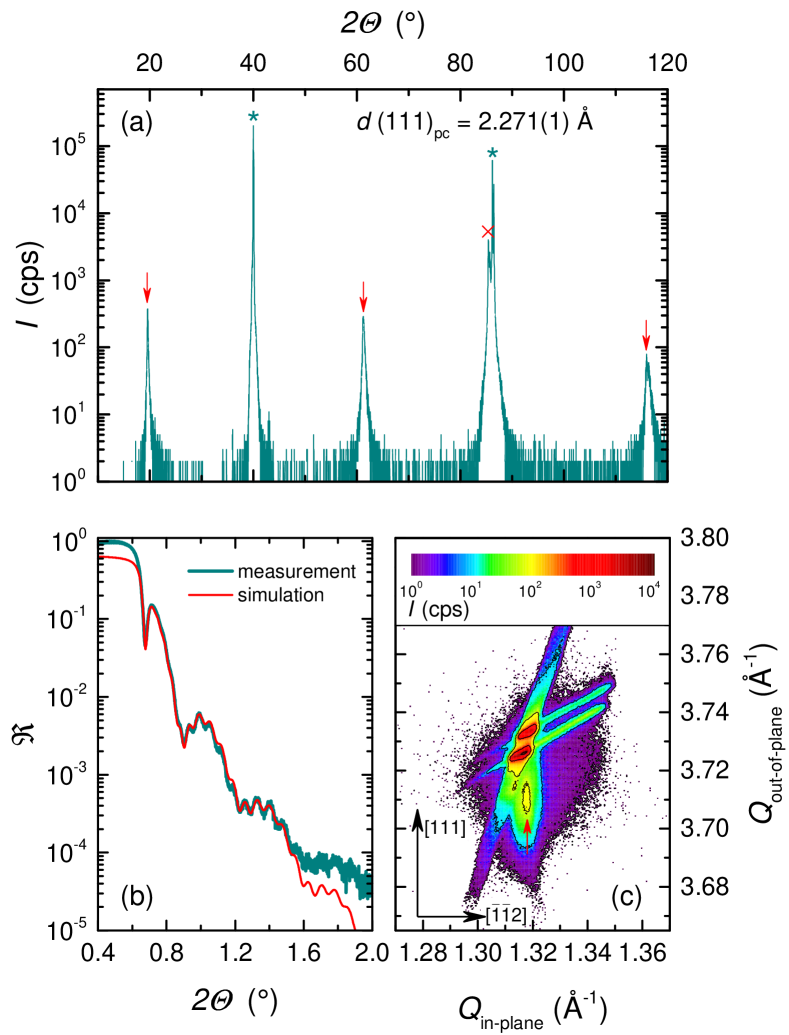
XRD measurements on (111) oriented thin films on (111) STO (see Figure 2 (a)) indicate an out-of-plane epitaxy. The presence of B-site ordering in films was evidenced by observation of (1/2 1/2 1/2) superstructure reflections, marked by red arrows in Figure 2 (a). The extracted pseudo cubic out-of-plane lattice parameter, , for all studied SCIO/STO films with is slightly larger than that measured for bulk SCIO, Mikhailova . The reason is the in-plane compressive strain due to the lattice mismatch between SCIO and STO. Reciprocal space mapping around the (112)-STO peak (see Figure 2 (c)) confirms the fully strained state of the film. Small angle XRR measurements in Figure 2 (b) indicate a large scale homogeneity of all SCIO films, , as well as for the STO capping layer, . The XRR signal can be well simulated with ReMagX ReMagX yielding extracted interface roughness of less then 2 nm.
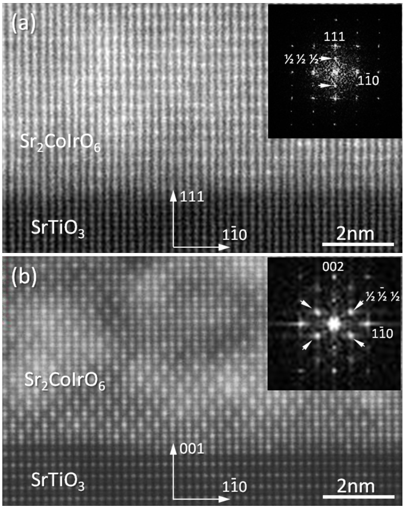
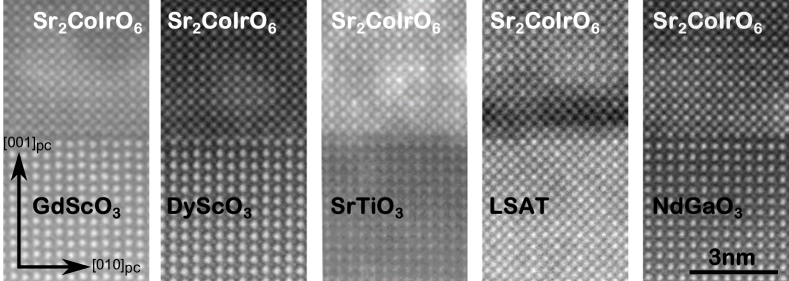
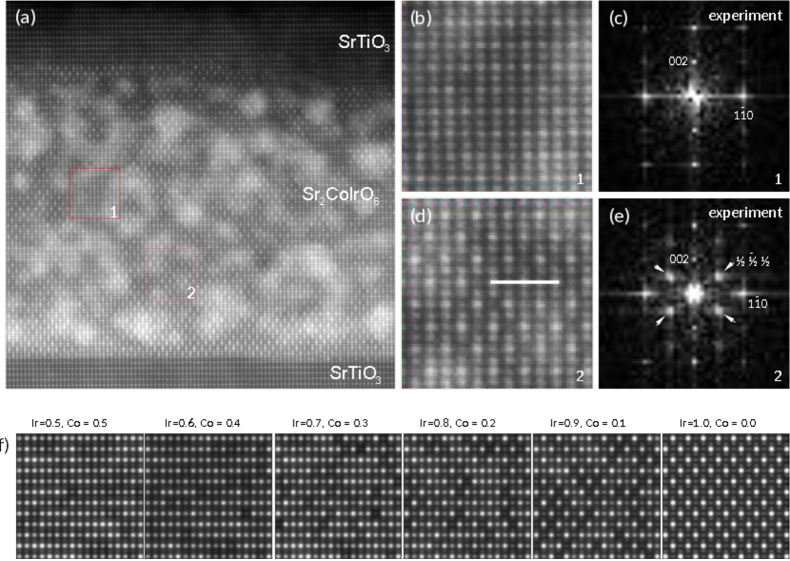
HR-STEM images and corresponding FFTs in Figure 3 confirm a high structural quality and the B-site ordering of SCIO films grown on (111) and (001) STO substrates. One can clearly see the pseudo-cubic symmetry with extra spots (white arrowheads) along the [111] direction due to the established B-site ordered superstructure. The SCIO/STO interfaces in look coherent in agreement with results from the reciprocal space map, thus, evidencing a fully strained state of the film. Moreover, no dislocations or other defects are observed. Also the B-site ordering is clearly seen in Figure 3 (b) since the atomic number of Ir is much larger than the atomic number of Co. The degree of Co/Ir ordering is estimated using HR-STEM image simulation to be more than 65% (see SM Figure S3) SM .
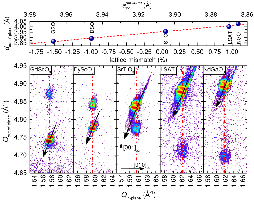
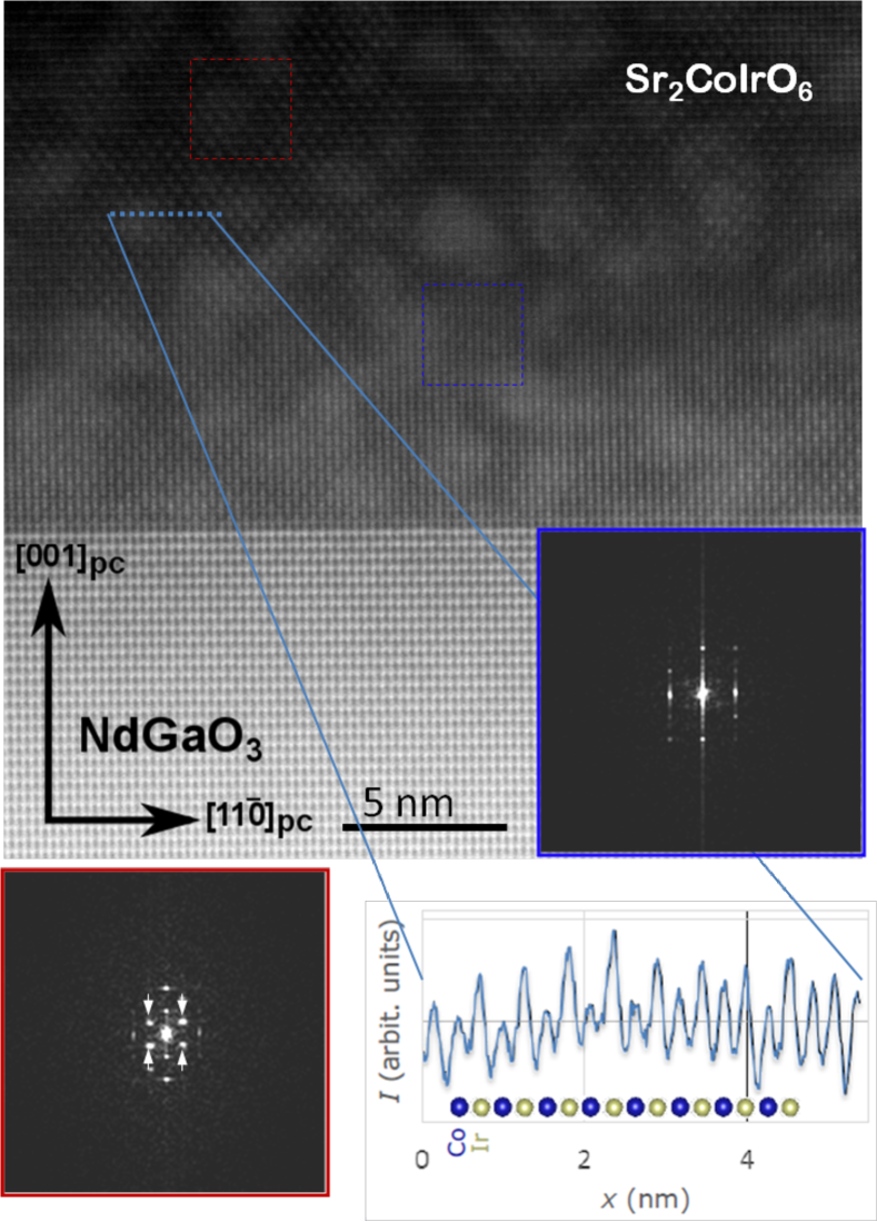
To realize a biaxial tensile strain along the [100] and the [010] direction, we used substrates of GdScO3 (GSO, ) and DyScO3 (DSO, ) in (001) orientation. To exert biaxial compressive strain the (001)-oriented SrTiO3 (STO, ), LSAT () and NdGaO3 (NGO, ) were used.
In the top panel of Figure 4 the evaluated linear relation between the out-of-plane film lattice parameter and the pseudo-cubic substrate lattice parameter is shown for STO(20 nm)/SCIO(20 nm) films. Within the linear elasticity theory this behavior indicates a fully strained state of films with the poisson’s ratio of . Reciprocal space mapping around each (pseudo) cubic (013) substrate peak (see Figure 4 (middle panel)) prove the fully strained state of each film grown on the used substrates. In addition, HAADF STEM images also verify the strained film/substrate (001) interfaces (see Figure 4 (bottom panel)), preserved up to thickness of SCIO film.
In the case of STO as substrate material the B-site ordering was investigated by a XRD scan in tilted geometry with parallel to <111> of STO and therefore, regarding to the small lattice mismatch between SCIO and STO, also nearly parallel to <111> of SCIO. The visible superstructure peaks in the collected XRD pattern (see Figure 5 (a)) could be well distinguished from the STO background, comparable to the results of the (111) oriented thin films (see Figure 2 (a)), and indicating well developed B-site ordering. A larger lattice mismatch and therefore bigger difference between the <111> directions of substrate materials compared to strained SCIO, in combination with peaks appearing already from the bare substrate material at the crucial positions, is a key reason, why this access is denied in case of the other used substrate materials.
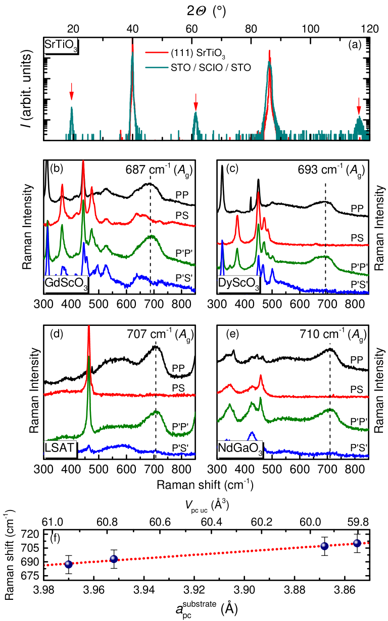
To clarify the B-site ordering state in such SCIO films we performed the polarization-dependent Raman spectroscopy (Figure 5 (b)-(e)) and compare the data with other ordered double perovskites of the same point group, e.g. La2CoMnO6 (LCMO). B-site-ordered LCMO obeys a monoclinic structure, for which theoretical lattice dynamical calculations Iliev predict stretching mode of the (Co/Mn)O6 octahedra (breathing mode) at . In contrast, the disordered LCMO obeys an orthorhombic structure and possesses the breathing mode. Similarly, we expect a (Co/Ir)O6 breathing mode with symmetry at a Raman shift, , for the B-site-ordered SCIO. In this case the mode should be present in Raman spectra, measured in parallel PP- and P’P’-configuration, and it is forbidden in the crossed scattering PS- and P’S’-configurationIliev ; Truong ; Meyer (the prime i ndicates measurements with an in-plane rotation of the sample by 45 around the [001] direction and provide an additional tool to test the epitaxy). For the disordered orthorhombic structure, the selection rules are oppositeIliev ; Truong ; Meyer . As one can see in Figure 5 (b)-(e), all films in our strain series exhibit a strong breathing mode at in the parallel PP- and P’P’-scattering configurations and only a weak (or none) intensity in the crossed PS- and P’S’-configuration. Thus, the symmetry and the B-site ordering can be concluded for all strained films grown on GSO, DSO, LSAT and NGO. Furthermore, the Raman shift of the breathing mode (see Figure 5 (f)) was found to depend linearly on the strain, . This is due to the change of the unit cell volume, , and of the phonon energy with strain. Note, that a smaller leads to a closer packing and, respectively, more energy is necessary. Kumar and KaurKumar , observed a similar behavior of the breathing mode in a strain relaxation series of the double perovskite La2NiMnO6/LaAlO3(001).
For selected films on GSO, STO and NGO substrates the B-site ordering was also studied on the micro scale by HAADF STEM measurements along the [110] direction (see supplementary material) SM . These measurements show that independent on strain there are regions with a high degree of B-site ordering, which alternate with regions with lower or no B-site ordering at all. Concluding, the epitaxial strain perpendicular to the [001] direction could neither improve nor weaken the B-site ordering in SCIO.
III.2 Magnetic properties
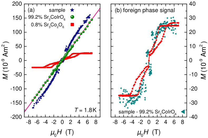
Separation of magnetic properties of thin films from the substrate magnetic contribution is generally difficult. A comparison with data on bulk SCIO Narayanan indicates, that a film with minimal thickness of 200 nm is required to get magnetic moment corresponding to 5 % of the moment of pure STO substrate at room temperature. Because fully strained (001) oriented SCIO films are stable for d50 nm, we focus here solely on thick () strained SCIO/STO(111)c films, cf. Figure 1. However, we identified a Sr3Co2O6 (SCO) second phase inclusion on the level 0.8 volume-%. For a quantitative determination of the SCO volume fraction, we have used the field dependent measurements of magnetization at lowest temperature (for more details, see supplemental material SM ). The foreign phase moments are saturated in a field of 7 T that has been applied in the measurement shown in Figure 6. Furth ermore, for our analysis of the difference between zero-field cooled (ZFC) and field cooled (FC) magnetization, it cancels out.
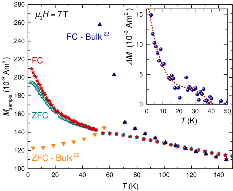
Previous investigation on polycrystalline SCIO revealed long-range magnetic order at 70 K, with ferromagnetic and antiferromagnetic components of the ordered magnetic moments, yielding to a pronounced difference in the FC and ZFC magnetization Narayanan . Figure 6 compares these literature data on polycrystalline SCIO (from Ref. Narayanan , indicated by triangles) with the FC and ZFC magnetization measurements of our thick (111) oriented SCIO film below 150 K. Compared to the polycrystal data, much weaker splitting between FC and ZFC is found and the maximum at 70 K in ZFC mode is absent. Taking the onset of the difference between FC and ZFC (see inset of Figure 6) as measure of magnetic order, an ordering temperature of 43 K would be estimated for the film, which is significantly reduced compared to the polycrystal. We speculate that epitaxial strain and/or better B-site order is responsible for the differ ence in the magnetic susceptibility behavior.
In strained (111) oriented thin films of the double perowskite Sr2FeMoO6 Hauser et al. found a similar decrease of the ordering temperature Hauser . Unfortunately, the thinner films of the (001) strain series could not be investigated by respective magnetization measurements and the evolution of the susceptibility behavior with strain remains therefore unknown.
III.3 Spectroscopic results
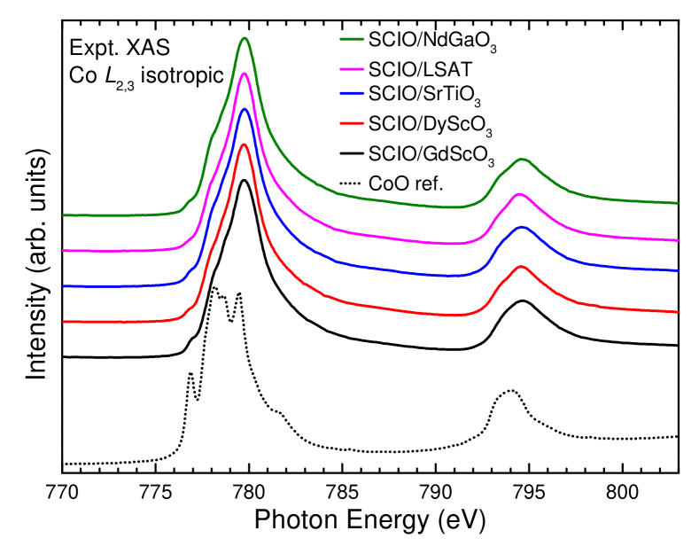
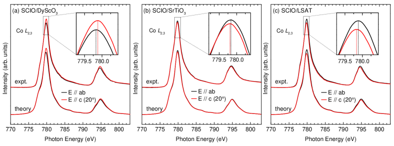
As mentioned in the previous section the magnetic signal for the samples of the (001) strain series are too weak to be detected in a conventional SQUID magnetometer. In order to investigate the electronic structure and its antiferromagnetic property of the SCIO thin films, we resort to polarization-dependent XAS. Optical measurements were done on the SCIO films capped by 2 nm thick STO Esser , which due to its high integrity and insulating properties Belenchuk protects SCIO films from degradation but still allows electrons to escape. We note that the polarization-dependent XAS is one of few techniques that can determine the magnetic axis of an antiferromagnetic ordered state in thin films. Haverkort2004 ; Csiszar2005 ; NatComms7 Figure 7 (a) and (b) show the experimental polarization-dependent Co XAS spectra of the most tensile strained SCIO thin films on GSO and the most compressive strained SCIO films on NGO, respectively, in this study, taken at 300 K. The spectra of the SCIO thin films on DSO, STO, and LSAT substrates are shown in Figure S9 of the SM SM . The spectra are dominated by the Co core-hole spin-orbit coupling which splits the spectrum roughly in two parts, namely the ( 776-784 eV) and ( 793-797 eV) white lines regions. The line shape strongly depends on the multiplet structure given by the Co 3-3 and 2-3 Coulomb and exchange interactions, as well as by the local crystal fields and the hybridization with the O 2 ligands. Unique to soft XAS is that the dipole selection rules are very sensitive in determining which of the 23 final states can be reached and with what intensity, starting from a particular 23 initial state ( for Co3+) PRL92 ; PRL102 ; PRB95 . This makes the technique extremely sensitive to the symmetry of the initial state, i.e., the spin, orbital and valence states of the ions.
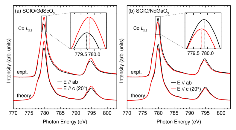
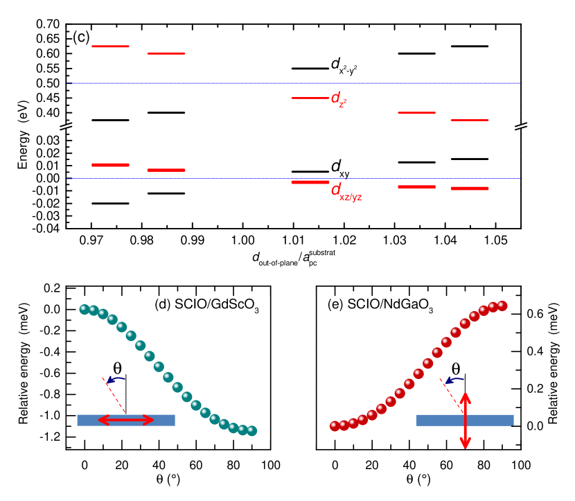
The experimental XAS spectra show that the Co valence state of these SCIO thin films is mainly 3+. Please be noted that for comparing with the calculated spectra the experimental spectra in Figure 7 (a) and (b) have been subtracted by 10% and 8% of Co2+, respectively. The experimental isotropic XAS spectra before subtracting Co2+ contributions can be found in Figure S8 of the SM SM . Further, the spectral features indicate a high spin (HS) state of the Co3+ ions PRL92 ; PRL102 ; PRB95 in the SCIO thin films which is independent of substrates underneath, i.e., a strain independent HS state. On the other hand, the orbital state in these SCIO thin films is quite different as indicated by the opposite sign of the polarization-dependent difference of spectra.Haverkort2004 ; Csiszar2005 For example, the intensity of the main peak is always larger for E c (20 than for E ab in the SCIO/GSO thin film, whereas it is always smaller in the SCIO/NGO thin film. Since these spectra were taken at 300 K whi ch is much higher than the magnetic ordering temperature of 43 K, the polarization contrast is caused solely by crystal field effects. Using the E vector of light parallel to the ab plane (black lines), we can reach the unoccupied Co 3 orbital states with xy/x2-y2 characters. With the E vector of light parallel c axis (red lines), we detect the unoccupied Co 3 orbital states with yz/zx/3z2-r2 characters. This indicates that the sign of the crystal field splitting is opposite in the two systems. This inference is further consolidated by the observed peak energy difference of the main line as depicted in the insets of Figure 7 (a) and (b). The peak position is higher for E c (20 than for E ab in the SCIO/GSO thin film, while it is lower in the SCIO/NGO thin film. All together, we derive that in the tensile strained SCIO/GSO thin films the orbital states with x/y-character are energetically favorable, whereas in the compressive strained SCIO/NGO thin films the orbital states with z-character are energetically favorable. This can be understood qualitatively as the applied strain from the substrates underneath induces a tetragonal distortion and causes the corresponding orbital state shift in energy.
For further confirming this orbital energy level diagram and knowing the corresponding magnetic anisotropy, we have simulated the XAS spectra using the well proven configuration interaction cluster model that includes the full atomic multiplet theory deGroot ; Tanaka . The calculations were performed using the XTLS 8.3 program Tanaka . For the calculation details, please see the SM SM . As displayed in the bottom of Figure 7 (a) and (b), the calculated spectra based on the HS Co3+ model with the energy diagram of the orbital state shown in Fig. 9 (c) can well reproduce the experimental spectra. We can safely conclude that a tensile strain stabilizes a ( + 3) state and a compressive stain stabilizes a ( + 3) state in SCIO thin films. We infer that the change of the anisotropy in the crystal field parameters in going from room temperature to low temperatures due to thermal contraction of the substrates is negligible, and that we therefore can use these XAS derived parameters also for the analysis of the low temperature magnetic properties (see the Supplemental Material for details). Accordingly, we can calculate the magnetic anisotropy energy as a function of the spin direction for each case as shown in Figure 7 (d) (tensile, SCIO/GSO) and (e) (compressive, SCIO/NGO).The magnitude of the exchange field was set to 4 meV in accordance with the the magnetic ordering temperature of 43 K. PRB95 This magnetic anisotropy energy is expressed as , where is the angle between the exchange field and the [001]pc, and is the azimuthal angle which is set to 45∘. We find for the SCIO/GSO (tensile) meV, meV, and meV, while for the SCIO/NGO (compressive) we obtain meV, meV, and meV. In other words, for the tensile strained SCIO/GSO thin film, the spin moment favors the in-plane direction with the energy difference of about 1.14 meV between the magnetic easy axis (, in the film plane) and hard axis (, perpendicular to the film), whereas for the compressive strained SCIO/NGO thin film, the spin moment favors the out-of-plane direction with the energy difference of about 0.64 meV between the magnetic easy axis (, perpendicular to the film) and hard axis (, in the film plane). Note that the evaluated strain-induced AFM magnetic anisotropy in SCIO films, i.e. in/out of plane for tensile/com-pressive stress, differs from that observed for ferromagnetic double perovskite films of La2CoMnO6, i.e. in/out of plane for compressive/tensile stress Galceran ; Lopez-Mir . The reason is unclear up to know and, likely, is related to the FM exchange interaction between Co2+ and Mn4+ ions accordiung to the second Goodenough-Kanamori-Anderson rule. This is a piece of useful information for understanding the magnetotransport properties of the SCIO thin films under different strains, see the discussion in the section of Magnetotransport.
III.4 Zero field transport properties
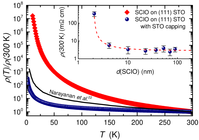
We now turn to the electrical resistivity of SCIO thin films. The temperature dependent measurements for a (111) oriented (SCIO) 30 nm thick SCIO film (with and without STO protective top layer) are shown in Figure 8. Similar to the bulk SCIO (Ref. Narayanan ), thin films also show an insulating behavior. The values of room temperature resistivity for the air protected and unprotected films were and , respectively. The reported bulk value (Ref. Narayanan ) was about 3 and 1.5 times larger, respectively. Upon cooling to 4 K, the electrical resistance of the unprotected film strongly increases, becoming several orders of magnitude larger than the resistance of the protectedfilm; the of the bulk SCIO lies in between. This indicates the importance of the STO capping layer to protect the (surface) properties of SCIO. As shown in the inset of Figure 8 the room temperature resistivity is almost independent on the film thickness for . Unfortunately, it was impossible to probe the thickness dependence at low temperatures. Fitting the data of the capped SCIO thin film between 250 and 300 K results in a charge gap of meV SM . Below 70 K, indicates variable range hopping behavior SM .
III.5 Magnetotransport within the (001) strain series
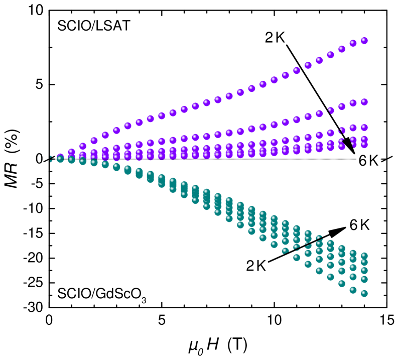
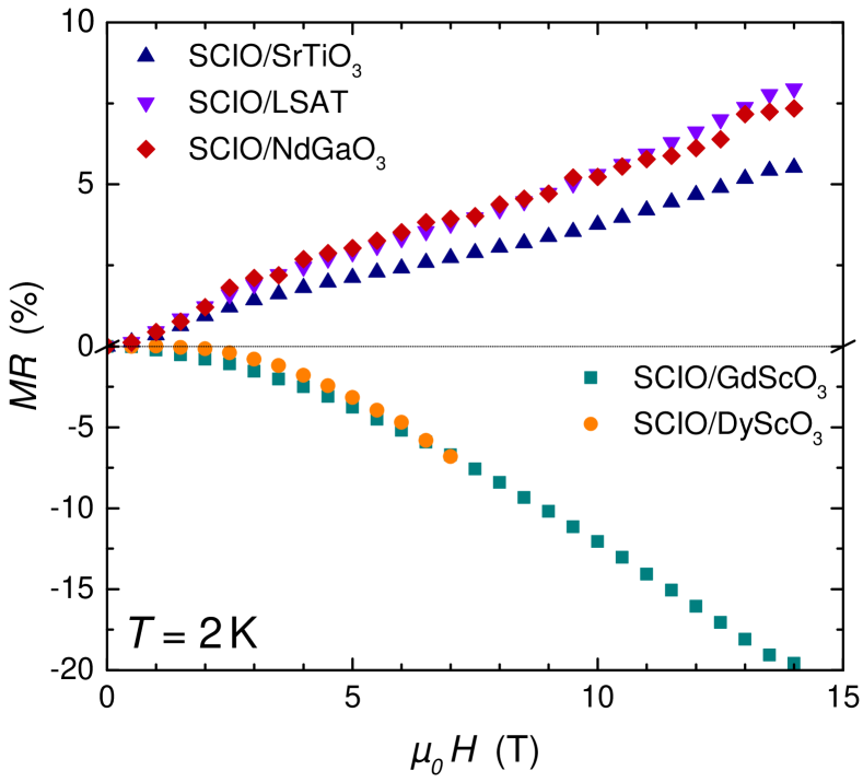
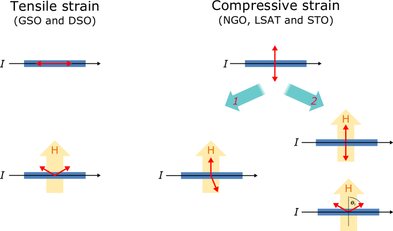
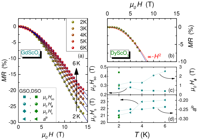
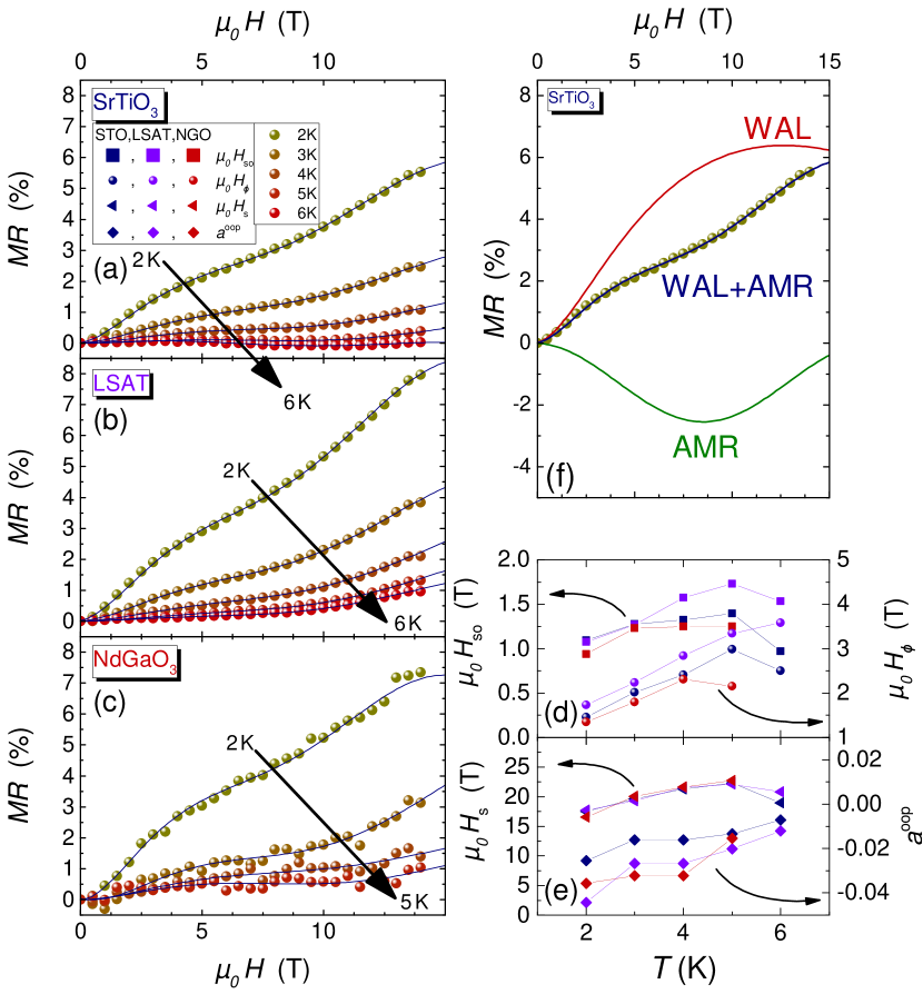
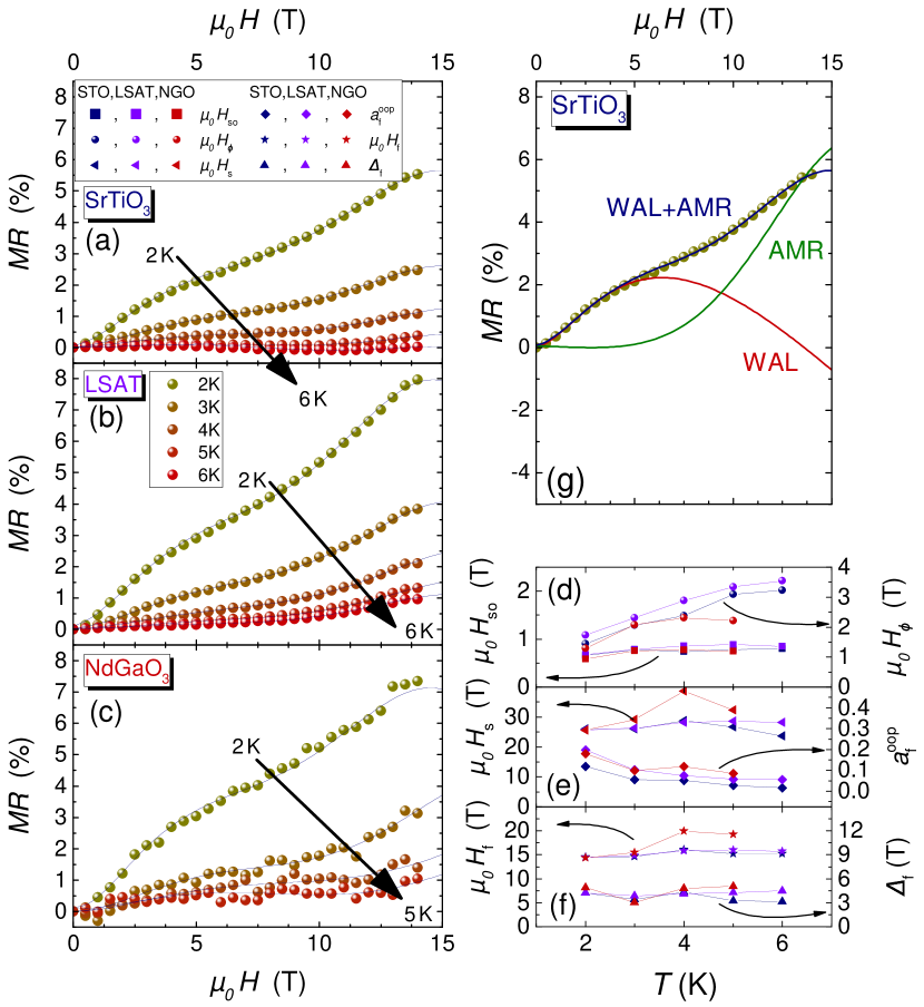
Considering the information on the magnetic anisotropy, obtained in the ”Spectroscopy” section, we can now address the magnetotransport properties of the SCIO thin films under different strains. Next, we focus on the low-temperature isothermal magnetoresistance (MR) of (001) strained SCIO thin films. As discussed previously in section C, the magnetic easy axis in this series changes from the ”in-plane” to the ”out-of-plane” as the strain changes from tensile to compressive. This change of the magnetic anisotropy has a direct influence on the magnetoresistance. As shown in Figure 9, MR below 6 K is positive for thin films grown under compressive strain on LSAT substrate and negative for those under tensile strain on GSO substrate. This indicates a direct relation between MR sign and magnetic anisotropy. This is further corroborated by the comparison of the MR at 2 K of all strained SCIO thin films, which, as shown in Figure 10, follow this trend. This observation suggests a strong influence of the anisotropic magnetoresistance (AMR) effect in combination with the reorientation of the AF M ordered Co sublattice in SCIO in an external transverse magnetic field.
In addition, structural disorder in combination with large spin orbit coupling will generate a quantum correction to MR due to weak anti-localization (WAL). Based on the Dresselhaus effekt Dresselhaus we used for the description of the WAL term of the MR a Dresselhaus like contribution with isotropic spin orbit scattering, see supplemental material SM . For the AMR contribution the orientation of the moments of Co sublattices in their AF ground state with respect to the field direction is important. For tensile strain at zero field the moments are oriented in the film plane and application of a transverse field leads to a continuous rotation of both sublattice moments out of the plane. This leads to a negative MR. For compressive strain, the moments of the two sublattices initially point parallel and antiparallel to the applied field. If there would be very weak coupling between the two sublattices, only the moments of the antiparallel sublattice would continuous ly rotate towards the applied field direction with increasing field. In the alternative case, upon increasing magnetic field the moments remain in their orientation until a spin-flip occurs (for a sketch, see supplemental material), followed by continuous rotation towards the field. Since there is no indication for a sharp spin flip, we modeled the MR behavior in a smeared spin flip scenario. For more details, we refer to supplemental material SM .
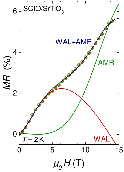
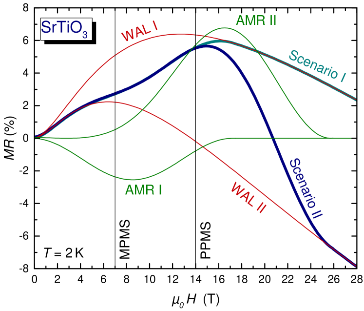
By combining AMR and WAL a valuable quantitative description of the measured MR is possible for all strained SCIO thin films. This is exemplified in Figure 11 for compressively strained SCIO. Within the smeared spin-flip scenario, a positive AMR contribution to the MR dominates between 10 and 24 T SM . As detailed in supplemental material, the obtained parameter for the WAL and AMR contributions within the smeared spin-flip scenario are more realistic compared to the assumption of very weak coupling between the two Co sublattices. To point out our key arguments: We expected a positive contribution from AMR and a temperature independent spin-orbit scattering field within the WAL contribution. Both is only the case in the smeared spin-flip scenario.
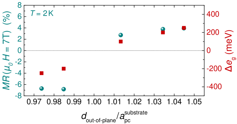
As indicated by Figure 12 the strain induced change of the Co d-level splitting, and respective change of moment orientation from in-plane (for tensile strain) to out-of plane (for compressive strain) goes hand in hand with a change of the MR from negative to positive. Due to the counteracting contributions of WAL and AMR effect in the samples with compressive strain, the absolute value of the MR is much smaller than for tensile strained samples, cf. Figure 10.
IV Conclusion
For the first time B–site ordered SCIO thin films have been grown on (111) oriented STO substrates and within a strain series also on various (pseudo) cubic (001) oriented substrates. Our electrical transport measurements of (111) oriented samples with and without an air protection layer out of STO indicated in comparison to literature results from reference Narayanan that the SCIO thin films degenerate in direct air contact. This leads us to the development of a four step in-situ lithographical process to investigate the temperature and magnetic field dependencies of the electrical transport properties for protected samples.
The complete strain transfer from the substrate to the thin film was checked in all cases of the (001) strain series by RSMs around the (013) substrate peak in combination with HAADF STEM images in [100] direction. The, at least partial, B–site ordering of the SCIO thin films was proven by XRD scans in tilted geometry as well as by polarization dependent Raman spectroscopy. HAADF STEM images in [110] direction of selected samples reinforce these results.
The magnetic properties were investigated with SQUID magnetometry. The AFM ordering temperature of the thick SCIO thin films is reduced in comparison to the bulk value ( Narayanan ). Using polarization dependent x-ray absorption spectroscopy at the Co edges, we revealed that the Co orbital occupation strongly depends on the strain in the SCIO thin films induced by the substrates. The tensile strained SCIO thin films stabilize the occupation of the minority orbital state with x/y character, whereas the compressive strained SCIO thin films favor the occupation of the minority orbital state with z character. Together with the calculations using the well proven configuration interaction cluster model, we were able to determine the magnetic easy axis change due to the induced strain from the substrates, and the sign and the magnitude of the magnetic anisotropy energy of the antiferromagnetically ordered high-spin Co3+ ions. We presented a quantitative model including the anisotropic magnetoresistance and weak anti-localization effects to explain the opposite behavior and its magnitude of the low-temperature magnetoresistance in the tensile strained from the compressive strained SCIO thin films.
Acknowledgements.
The authors like to thank S. Meir for developing the shadow mask argon ion etching method at Augsburg University and B. Meir for the support with it. We thank R. Pentcheva and P. Seiler for stimulating discussions. The work at Augsburg was supported by the Deutsche Forschungsgemeinschaft (DFG) through SPP 1666 and TRR 80. The research in Dresden was partially supported by the DFG through SFB 1143 and the study in Göttingen through SFB 1073 (TP A02).References
- (1) S. Vasala and M. Karppinen, Prog. Solid State Ch.43, (2015) 1.
- (2) A. Ohtomo, S. Chakraverty, H. Mashiko, T. Oshima, and M. Kawasaki, J. Mater. Res. 28 (2013) 5.
- (3) M. T. Anderson, K. B. Greenwood, G. A. Taylor, and K. R. Poeppelmeier, Prog. Solid State Chem. 22 (1993) 197.
- (4) S. Chakraverty, A. Ohtomo, D. Okuyama, M. Saito, M. Okude, R. Kumai, T. Arima, Y. Tokura, S. Tsukimoto, Y. Ikuhara, M. Kawasaki, Phys. Rev. B 84 (2011) 064436.
- (5) D. Serrate, J. M. D. Teresa, and M. R. Ibarra, J. Phys.-Condens Mat. 19, (2007) 023201.
- (6) M. P. Singh, K. D. Truong, and P. Fournier, Appl. Phys. Lett. 91, (2007) 042504.
- (7) H. L. Feng, M. Arai, Y. Matsushita, Y. Tsujimoto, Y. Yuan, C. I. Sathish, J. He, M. Tanaka, and K. Yamaura, J. Solid State Chem. 217 (2014) 9.
- (8) B. J. Kim, H. Jin, S. J. Moon, J.-Y. Kim, B.-G. Park, C. S. Leem, J. Yu, T. W. Noh, C. Kim, S.-J. Oh, J.-H. Park, V. Durairaj, G. Cao, E. Rotenberg, Phys. Rev. Lett. 101, (2008) 076402.
- (9) B. J. Kim, H. Ohsumi, T. Komesu, S. Sakai, T. Morita, H. Takagi, and T. Arima, Science 323, (2009) 1329.
- (10) Y. F. Nie, P. D. C. King, C. H. Kim, M. Uchida, H. I. Wei, B. D. Faeth, J. P. Ruf, J. P. C. Ruff, L. Xie, X. Pan, C. J. Fennie, D. G. Schlom, and K. M. Shen, Phys. Rev. Lett. 114, (2015) 016401.
- (11) G. Jackeli, and G. Khaliullin, Phys. Rev. Lett. 102, (2009) 017205.
- (12) A. Kitaev, Ann. Phys. 321, (2006) 2.
- (13) S. M. Winter, A. A. Tsirlin, M. Daghofer, J. van den Brink, Y. Singh, P. Gegenwart, and R. Valenti, J. Phys.: Condens. Matter 29, (2017) 493002.
- (14) K. Momma, and F. Izumi, J. Appl. Crystallogr. 44 (2011) 1272.
- (15) D. Mikhailova, N. Narayanan, W. Gruner, A. Voss, A. Senyshyn, D. M. Trots, H. Fuess, and H. Ehrenberg, Inorg. Chem. 49 (2010) 10348.
- (16) S. Kanungo, K. Mogare, B. Yan, M. Reehuis, A. Hoser, C. Felser, and M. Jansen, Phys. Rev. B 93, (2016) 245148.
- (17) G. Cao, A. Subedi, S. Calder, J.-Q. Yan, J. Yi, Z. Gai, L. Poudel, D. J. Singh, M. D. Lumsden, A. D. Christianson, B. C. Sales, and D. Mandrus, Phys. Rev. B 87, (2013) 155136.
- (18) G. Cao, T. F. Qi, L. Li, J. Terzic, S. J. Yuan, L. E. DeLong, G. Murthy, and R. K. Kaul, Phys. Rev. Lett. 112, (2014) 056402.
- (19) L. T. Corredor, G. Aslan-Cansever, M. Sturza, Kaustuv Manna, A. Maljuk, S. Gass, T. Dey, A. U. B. Wolter, Olga Kataeva, A. Zimmermann, M. Geyer, C. G. F. Blum, S. Wurmehl, and B. Büchner, Phys. Rev. B 95, (2017) 064418.
- (20) F. Hammerath, R. Sarkar, S. Kamusella, C. Baines, H.-H. Klauss, T. Dey, A. Maljuk, S. Ga , A. U. B. Wolter, H.-J. Grafe, S. Wurmehl, and B. Büchner, Phys. Rev. B 96, (2017) 165108.
- (21) J.-M. Carter, V. V. Shankar, M. A. Zeb, and H.-Y. Kee, Phys. Rev. B 85, (2012) 115105.
- (22) N. Narayanan, D. Mikhailova, A. Senyshyn, D. M. Trots, R. Laskowski, P. Blaha, K. Schwarz, H. Fuess, and H. Ehrenberg, Phys. Rev. B 82 (2010) 024403.
- (23) M. Schneider, D. Geiger, S. Esser, U. Pracht, C. Stingl, Y. Tokiwa, V. Mosneaga, I. Sheikin, J. Mravlje, M. Scheffler, and P. Gegenwart, Phys. Rev. Lett. 112, (2014) 206403.
- (24) V. Moshnyaga, I. Khoroshun, A. Sidorenko, P. Petrenko, A. Weidinger, M. Zeitler, B. Rauschenbach, R. Tidecks, and K. Samwer, Appl. Phys. Lett. 74 (1999) 2842.
- (25) M. Jungbauer, S. Hühn, M. Michelmann, E. Goering, und V. Moshnyaga, J. Appl. Phys. 113 (2013) 17D709.
- (26) S. Macke, S. Brück, P. Audehm, M. Harlander, and E. Goering, ReMagX: X-ray Magnetic Reflectivity Tool, 2009, Available at http://www.mf.mpg.de/remagx.html.
- (27) See supplemental material for details concerning the in-situ lithographical prozess, additional structural information, the foreign phase determination, details of the zero field transport properties as well as the magnetoresistance modell and additional XAS spectra.
- (28) M. N. Iliev, M. V. Abrashev, A. P. Litvinchuk, V. G. Hadjiev, H. Guo, and A. Gupta, Phys. Rev. B 75 (2007) 104118.
- (29) K. D. Truong, J. Laverdière, M. P. Singh, S. Jandl, and P. Fournier, Phys. Rev. B 76, (2007) 132413.
- (30) C. Meyer, S. Hühn, M. Jungbauer, S. Merten, B. Damaschke, K. Samwer, and V. Moshnyaga, J. Raman Spectrosc. 48, (2017) 46.
- (31) D. Kumar, und D. Kaur, J. Alloy. Compd. 554, (2013) 277.
- (32) A. J. Hauser, R. E. A. Williams, R. A. Ricciardo, A. Genc, M. Dixit, J. M. Lucy, P. M.Woodward, H. L. Fraser, and F. Yang, Phys. Rev. B 83, (2011) 014407.
- (33) Sebastian Esser, Dissertation (2018),University of Augsburg.
- (34) A. Belenchuk, O. Shapoval, V. Roddatis, V. Bruchmann-Bamberg, K. Samwer, and V. Moshnyaga, Appl. Phys. Lett. 109, 232405 (2016).
- (35) M. W. Haverkort, S. I. Csiszar, Z. Hu, S. Altieri, A. Tanaka, H. H. Hsieh, H.-J. Lin, C. T. Chen, T. Hibma, and L. H. Tjeng, Phys. Rev. B 69, (2004) 020408(R).
- (36) S. I. Csiszar, M. W. Haverkort, Z. Hu, A. Tanaka, H. H. Hsieh, H.-J. Lin, C. T. Chen, T. Hibma, and L. H. Tjeng, Phys. Rev. Lett. 95, (2005) 187205.
- (37) C.-Y. Kuo, Z. Hu, J. C. Yang, S.-C. Liao, Y. L. Huang, R. K. Vasudevan, M. B. Okatan, S. Jesse, S. V. Kalinin, L. Li, H. J. Liu, C.-H. Lai, T. W. Pi, S. Agrestini, K. Chen, P. Ohresser, A. Tanaka, L. H. Tjeng, and Y. H. Chu, Nat. Comms. 7, (2016) 12712.
- (38) Z. Hu, H. Wu, M. W. Haverkort, H. H. Hsieh, H.-J. Lin, T. Lorenz, J. Baier, A. Reichl., I. Bonn, C. Felser, A. Tanaka, C. T. Chen, and L. H. Tjeng, Phys. Rev. Lett. 92, (2004) 207402.
- (39) C. F. Chang, Z. Hu, H. Wu, T. Burnus, N. Hollmann, M. Benomar, T. Lorenz, A. Tanaka, H.-J. Lin, H. H. Hsieh, C. T. Chen, and L. H. Tjeng, Phys. Rev. Lett. 102, (2009) 116401.
- (40) R. Galceran, L. Lopez-Mir, B. Bozzo, J. Cisneros-Fernandez, J. Santiso, L. Balcells, C. Frontera and B. Martinez, Phys. Rev. B 93, 144417 (2016).
- (41) L. Lopez-Mir, R. Galceran, J. Herrero-Martin, B. Bozzo, J. Cisneros-Fernandez, E.V. Pannunzio Miner, A. Pomar, L. Balcells, B. Martinez, and C. Frontera, Phys. Rev. B 95, 224434 (2017).
- (42) S. Agrestini, C.-Y. Kuo, D. Mikhailova, K. Chen, P. Ohresser, T. W. Pi, H. Guo, A. C. Komarek, A. Tanaka, Z. Hu, and L. H. Tjeng, Phys. Rev. B 95, (2017) 245131.
- (43) F. M. F. de Groot, J. Electron Spectrosc. Relat. Phenom. 67, (1994) 529.
- (44) A. Tanaka, and T. Jo, J. Phys. Soc. Jpn. 63, (1994) 2788.
- (45) P. D. Dresselhaus, C. M. A. Papavassiliou, R. G. Wheeler, and R. N. Sacks, Phys. Rev. Lett. 68, (1992) 106.
- (46) R. R. Birss, Symmetry and magnetism, Band 863, North-Holland Amsterdam, (1964).
- (47) P. K. Muduli, K.-J. Friedland, J. Herfort, H.-P. Schönherr, and K. H. Ploog, Phys. Rev. B 72, (2005) 104430.
Supplemental Material
In this Supplemental Material we provide a detailed description of the in-situ lithographical process, additional HAADF STEM images in [110] direction to clarify the B–site ordering and x-ray characterization as well as the field dependence of the magnetization of the sample measured in the conventional SQUID magnetometer to estimate the volume fraction of the magnetic impurity phase. Furthermore more details are given on the electronic transport properties, including a detailed evaluation of the field dependence of the magnetoresistance by combining weak anti-localization and AMR effect, and details to the XAS spectra and the configuration interaction cluster calculation.
In-situ lithographical process
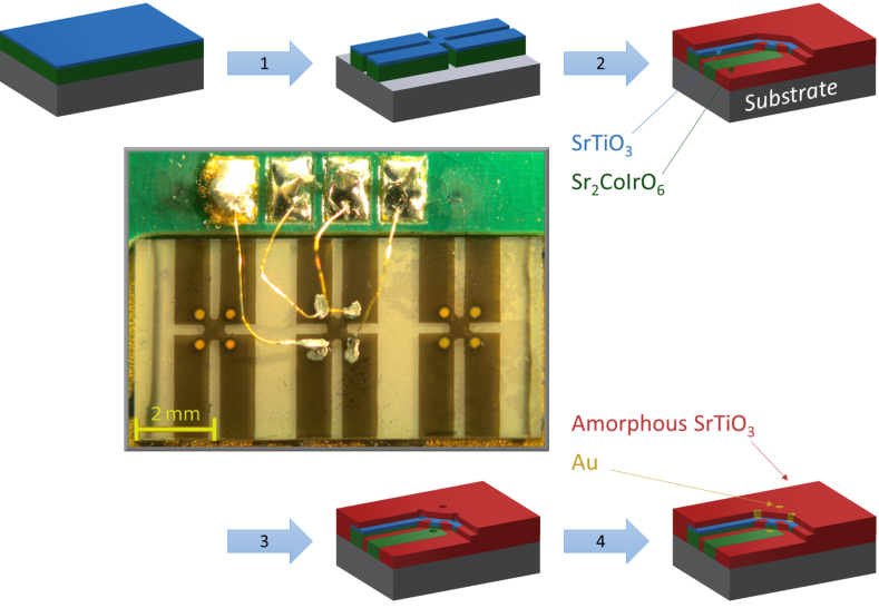
As mentioned in the main text we developed a four step method (sketched in Figure S1) with the following procedure to exclude an air exposure of the samples during the lithographic process:
-
1.
A van der Pauw measurement geometry is structured by using a shadow mask argon ion etching technique.
-
2.
The shadow mask is removed and for air protection a thick amorphous STO layer is ablated by pulsed laser deposition using a KrF (248 nm) excimer laser focused into a vacuum chamber to an energy density of 2-3 J/cm2 at the target at room temperature with an O2 background gas pressure of .
-
3.
A second shadow mask argon ion etching process digs contact holes through the STO cappings into the SCIO layer at the contact pads of the Van der Pauw measurement geometry.
-
4.
Those holes are filled with RF sputtered gold through the holes of the second shadow mask.
A structured and contacted sample is shown in the photo of Figure S1.
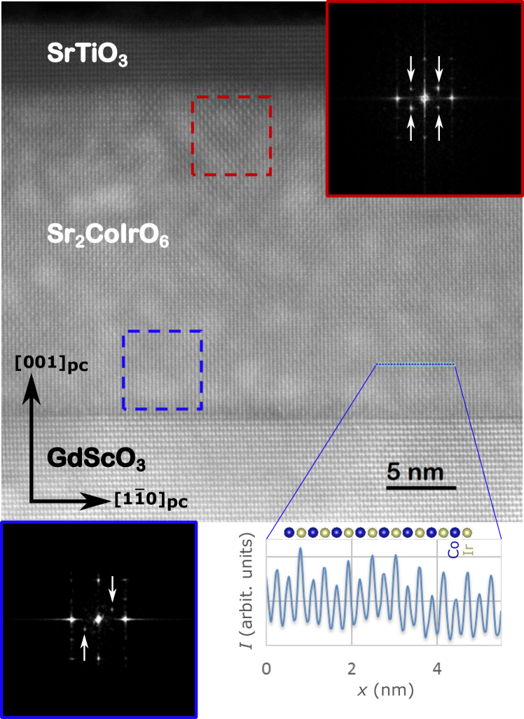
HAADF STEM measurements in [110] direction
To verify the B-site ordering of the samples on the micro scale, HAADF STEM measurements in [110] direction were performed on the SCIO samples grown on (001) oriented NGO, STO and GSO (see Figure S3, S4 and S5). As shown in Figure S2 this special direction provides an alternating arrangement of Co and Ir pillars only in a well ordered double perowskite structure.
Due to the good -contrast S_Hartel () of the HAADF mode, the difference between Co and Ir is clearly visible. The theoretical intensity ratio is and therefore line scans can already provide the desired information about the B-site ordering.
In our case most parts of the sample seems to be in a well ordered state, supporting the results shown in the main text.
In order to estimate the degree of B-site ordering we have performed a simulation of HR-STEM images for different occupancies of the corresponding columns with Co and Ir atoms. The results are shown in Fig. S3. The simulations allow us to estimate the degree of Co/Ir ordering to be 80-90%. Moreover, our HR-STEM images also show areas which do not have pronounced difference in the intensity of Ir/Co atomic columns. The corresponding FFT pattern also do not reveal the superstructure spots. In general, TEM is an essentially local method. However, the images of all studied films demonstrate a very similar ratio of ordered and disordered areas, which is at least . Thus, we can conclude that the degree of Co/Ir ordering is higher than 65%. Similar results were also reported for the bulk SCIO material (13.2% foreign B species occupation) S_Narayanan .
Identification of foreign phase within the SCIO sample for SQUID measurements and estimation of its relative volume fraction
Figure S6 shows the XRD pattern of the thick (111) oriented SCIO sample, which was used to probe the magnetic properties with the SQUID magnetometer. The additional peak at could be identified as tetragonal or orthorhombic Sr3Co2O6-δ (SCO). The further non substrate peaks belong to (111) oriented Sr2CoIrO6. The clearly visible super lattice peaks (marked by red arrows) indicate well developed B-site ordering. The thin film is still fully strained, as evidenced by the extracted out-of-plane lattice constant, which is the same as for thinner samples.
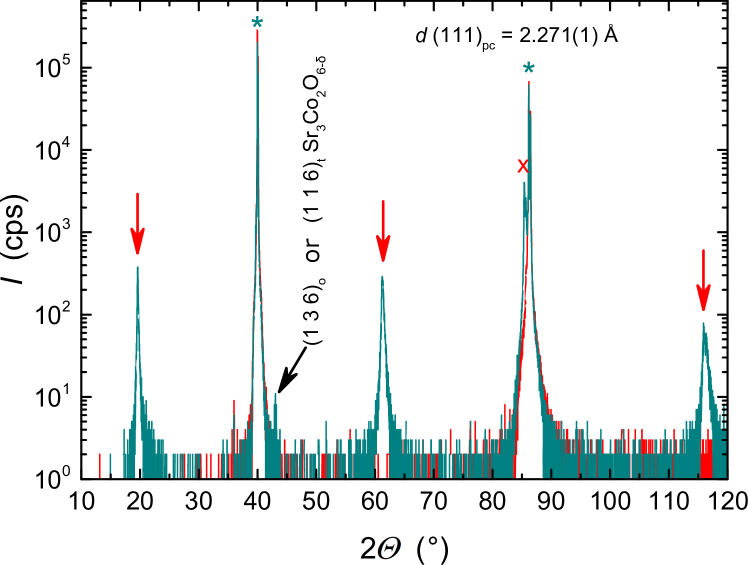
For a quantitative determination of the volume fraction of the Sr3Co2O6-δ foreign phase we could use the literature data of the field dependence of its magnetization from reference S_Wang . To describe our measured thin film magnetization (blue stars in Figure S7 (a)) a volume weighted superposition of SCIO and Sr3Co2O6-δ has been assumed. The estimated foreign phase fraction is (see Figure S7 (b)) and the pure SCIO signal follows in good agreement with the literature data from reference S_Narayanan a linear behavior.
XAS spectra and configuration interaction cluster calculation
Figure S8 shows the experimental isotropic Co XAS spectra of the SCIO thin films on GSO, DSO, STO, LSAT and NGO substrates taken at 300 K,
together with a standard Co2+ spectrum from CoO. The foot of the main line of the SCIO thin films at 776.9 eV is due to Co2+ contributions. Comparing the intensity ratio of the foot (776.9 eV) and the main line (779.74 eV), we derive 10 %, 7 %, 9 %, 6 %, and 8 % of Co2+ impurities from the SCIO thin films on GSO, DSO, STO, LSAT and NGO substrates, respectively. The isotropic XAS spectra were obtained via the formula of , where is the spectrum with the E parallel to the [001]pc surface normal extracted from . and are the spectra measured with E 20∘ off the [001]pc surface normal and E the [001] surface normal, i.e. E ab, respectively.
The x-ray absorption (XAS) spectra were calculated using the well established configuration interaction cluster model that includes the full atomic multiplet theory and the local effects of the solid S_deGroot ; S_Tanaka . It accounts for the intra-atomic Co and Coulomb and exchange interactions, the atomic and spin-orbit couplings, the O -Co hybridization and the local ionic crystal field. The calculations were done using the program XTLS 8.3 S_Tanaka . We have considered a CoO6 cluster. Parameters for the multipole part of the Coulomb interactions were given by 80% of the Hartree-Fock values for the and Slater integrals, while the monopole parts (, ) as well as the O -Co charge transfer energy were adopted from typical values for Co3+ S_PRL92 ; S_PRL102 ; S_PRB95 . The hopping integrals between the Co and O were calculated for the various Co-O bond lengths according to Harrison’s description. The ionic crystal field splitting of the and levels is set to be 0.5 eV for all SCIO thin films. Due to the epitaxial strain from the substrates, the levels are split into a and a with an energy difference of , and the levels are split into a doublet ( and ) and a singlet () with an energy difference of . The and were tuned to fit the experimental spectra: = -0.25 (GSO), -0.2 (DSO), 0.1 (STO), 0.2 (LSAT), and 0.25 (NGO) eV; = -0.03 (GSO), -0.018 (DSO), 0.008 (STO), 0.019 (LSAT), and 0.023 (NGO) eV. We show the experimental and calculated polarization-dependent Co XAS spectra of the SCIO thin films on DSO, STO, and LSAT substrates in Figure S9 (a), (b), and (c), respectively. Those results for the thin films on GSO and NGO are shown in Figure 7 of the main text. We argue that these XAS derived parameters can be used for the analysis of the low temperature magnetic properties since the change of the anisotropy in the crystal field parameters in going from room temperature to low temperatures due to thermal contraction of the substrates is negligible as we will explain now. From literature we can find the following thermal expansion coefficients for the substrates: GSO=1.09x10⁻⁵ (K-1), DSO=0.84x10⁻⁵ (K-1), STO=0.9x10⁻⁵ (K-1), LSAT=0.82x10⁻⁵ (K-1), NGO=0.9x10⁻⁵ (K-1). We then can estimate the substrate lattice constants at, for example, 5 K. Knowing that the SCIO films are fully strained, and knowing their Poisson ratio (from the data displayed in Fig. 4) together with the volume change of the bulk SCIO from 300 K (238.56 ) to 5 K (237.09 ) S_Mikhailova , we can subsequently estimate the out-of-plane lattice constants of the SCIO films at 5 K. We thus find that the c/a ratio at 5 K on GSO, DSO, STO, LAST, and NGO is 0.9766, 0.9855, 1.0141, 1.0363, and 1.045, respectively. This is marginally different from the values at 300 K, namely 0.9751, 0.9858, 1.0141, 1.0369, and 1.0451. Thus the anisotropy due to the crystal field at 5 K is practically the same as that at 300K. Please be noted that for comparing with the calculated spectra the experimental spectra in Figure S9 (a), (b), and (c) have been subtracted by 7 %, 9 % and 6 % of Co2+ impurities, respectively. For the simulations of the magnetic anisotropy energy as a function of the spin direction, an exchange field is applied on the Co ion.
Zero field transport properties
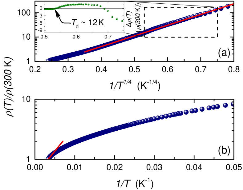
We analysed the high temperature electrical resistance behavior of the air protected thin film in a simple thermal activation scenario as shown in Figure S10 (b) and extracted as transport gap size . The deviation from Arrhenius type behavior sets in at and for we could describe our measurement in a good agreement with a three-dimensional variable-range hopping (VRH) model as introduced by Mott for disordered systems S_Mott (see Figure S10 (a)). At we observe a small kink and deviation from VRH (see inset of Figure S10 (a) and Figure S11). This deviation is not induced by the quantum correction due to weak anti-localization (WAL), because such correction would lead to a negative contribution (positive derivative of ) being logarithmic in temperatu re S_Bergmann ; S_Anderson , as found below (see Figure S11). Thus, it is likely, that the positive contribution results from the magnetic ordering of the Co sublattice, as it could be found in a similar way in the resistivity along the c-axis in the related perovskite Sr2IrO4 S_Fruchter , but this assumption needs to be substantiated by further investigations.
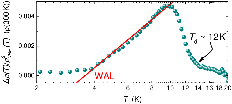
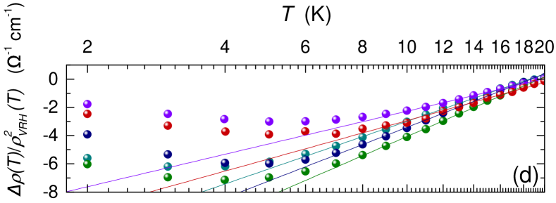
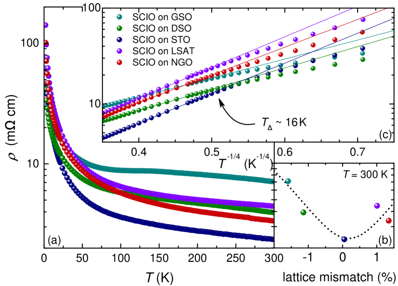
Figure S12 (a) shows temperature dependent transport measurements of various (001) strained samples. The overall insulating behavior is not changed by epitaxial strain and also the deviation temperature from the low temperature 3D VRH scenario does not change significantly (see Figure S12 (b)). Our analysis of the high temperature behavior within the simple thermal activation of electronic transport scenario reveals a transport gap size which is reduced compared to the (111) oriented sample.
Another obvious effect of the strain is the evolution of the specific resistance at room temperature , which increases with increasing absolute strain strength , whereby is the lattice mismatch (see Figure S12 (c)). Compared to other transition metal oxides this effect is not unexpected and was found (with other power law behavior) also in La0.7Ca0.3MnO3 S_Wu and ZnO S_Ghosh .
Magnetotransport for (001) strained SCIO
Historically motivated by the Dresselhaus effect the WAL quantum corrections leads to S_Dresselhaus
| (1) |
in which we assume isotropic spin orbit scattering and where with the Digamma function . Consequently the WAL will influence the magnetoresistance as follows
| (2) |
Furthermore at lowest temperature the AFM ordering of the Co sublattice and its response to external magnetic field by the anisotropic magnetoresistance (AMR) effect needs to be taken into account. For the description of the field dependence of the AMR effect we follow the Ansatz of Birss S_Birss and Muduli et al. S_Muduli . The components of the resistance tensor are written in a taylor expansion of the components of the magnetization direction for each of the two Co sublattices ()
| (3) |
in which the expansion coefficients have to preserve the lattice symmetry S_Limmer . Due to the Onsager theorem equation (3) could be divided into a symmetric and an antisymmetric part, where the symmetric part describes the generalized magnetoresistance and the antisymmetric part the generalized Hall effect S_McGuire . For in-plane current direction, a symmetry and Taylor expansion until second order in magnetization, the symmetric part of equation (3) reduces to
| (4) |
where is a diagonal matrix. With the assumption that the field dependence of equation (4) is mainly located in the magnetization orientation, the AMR effect will influence the magnetoresistance as follows
| (5) |
which leads in total to
| (6) |
We now need to model the magnetic response of the AFM ordered Co sublattice in case of an external field perpendicular to the thin film plane. Due to the change of magnetic easy axis with inversion of the strain direction we need to setup a separate model for each strain direction. Furthermore we have to distinguish between to scenarios in case of the external magnetic field parallel to the magnetic easy axis (quasi independent FM sublattices vs. classical spin-flip). Figure S13 illustrates all of our scenarios.
For the tensile strain case we assume, that the angle between the magnetization and the current direction is proportional to the external magnetic field and reaches at the saturation field . Then the magnetisation direction could be described by
| (7) |
where () is a unit vector in out-of-plane (in-plane) direction and the Heaviside step function. The field dependence of the MR in tensile strained case therefore leads to
| (8) |
where .
This model enables us to describe in good consistency the collected MR data which are shown in Figure S14.
As expected the spin-orbit scattering field is nearly temperature independent, whereas the inelastic scattering field follows a power law behavior with . The saturation field also slightly increases with temperature. This is reasonable because in the mean field approximation the argument of the Brillouin function needs to be constant to reach the saturation.
In case of compressive epitaxial strain we have to distinguish between two possibilities. In the first scenario the AFM coupling between the two sublattices is very weak, which enables us to deal with two quasi independent FM sublattices. In this scenario only the () sublattice, where the magnetization is aligned antiparallel to the external field, is influenced and has to be taken into account in equation (5). As in the tensile strained case we model its magnetization direction by a linear coupling of the external magnetic field to the angle between magnetization and the current direction. This leads to
| (9) |
and thereby to the following field dependence of MR
| (10) |
where .
In the other possible scenario for the (001) compressive strained SCIO samples we want to use a spin-flip scenario with a spin-flip field followed by a continues rotation as in the other two cases. In this scenario the magnetisation direction could be modeled with
| (11) |
where is the spin-flip angle as defined in Figure S13. With this the field dependence of the MR in the spin-flip scenarios turns out to be
| (12) |
with . Due to fact that we did not observed any sharp jump in the MR data (see Figure S15 or S16) the spin-flip field needs to be smeared out by , which is justifiable because due to the incomplete B-site ordering a multi domain structure with different magnetic environments will be develop, resulting in slightly different spin-flip fields. With a smeared out step function localized at the field dependence of the MR turns out to be
| (13) |
To select the more realistic scenario we analyze the obtained fitting parameters shown in Figure S15 (d) - (e) and S16 (d) - (f) in comparison to the values and temperature behaviors obtained for tensile strained samples (see Figure S14 (c) - (d)).
Concerning the WAL part of the MR, the results obtained in the spin-flip scenario (II) are closer to those of the tensile strained case (TSC) than those of the quasi independent FM sublattice scenario (I) and therefore favoring the spin-flip scenario. In more detail the spin-orbit scattering field in scenario I is twice as big as in TSC and not temperature independent. On the other hand, for the second scenario the magnitude of is similar to the TS and also its temperature behavior is as expected. The inelastic scattering field follows in both cases the same linear behavior as in TSC, but the slope (TSC , I , II ) and also the absolute values are in the second scenario closer to those obtained in TSC.
Furthermore the spin-flip scenario is supported by the results of the AMR parts of the MR fits. Certainly strain influences the components of the galvanomagnetic tensor and therefore we did not restrict the prefactors and for the fits done in Figure S15 and S16. However, in principle they are linked to each other by and should be therefore positive because is negative. In case of the spin-flip scenario is positive over the whole temperature range and at least at the relation is satisfied. Nevertheless the temperature behaviors of and are slightly different. In contrast to this, the prefactor in scenario I is unexpectedly negative and much smaller (one orde r of magnitude) then in scenario II and also the increase of the saturation field with temperature is in this scenario much stronger than in scenario II () and in the TSC ().
Another argument for the validity of the spin-flip scenario is the temperature independence of the spin-flip field and the smearing of the spin-flip field . For a clear separation between the two scenarios we want to propose two experiments:
-
1.
By measuring the MR up to fields above the saturation field the AMR part cancels out of the MR and only the WAL part is remaining (see Figure S17). This region could be fitted separatly, using only the WAL formula, equation (2), and after subtraction of it from the total MR signal the remaining part could be analyzed in both ways.
-
2.
By using a STO buffer layer on a (001) piezoelectrical Pb(Mg1/3Nb2/3)0.72Ti0.28O3 (PMN-PT) substrate S_Doerr it should be possible to build a sample (STO/SCIO/STO/PMN-PT) in which a gate voltage could switch between the two different strain states in-situ. This could be used to determine in a first measurement in tensile configuration the WAL part, which than could be subtracted in the second measurement of MR in compressive configuration. As in the first proposed experiment the remaining part could be analyzed in both possible scenarios.
References
- (1) P. Hartel, H. Rose, and C. Dinges, Ultramicroscopy 63, (1996) 93.
- (2) K. Momma, and F. Izumi, J. Appl. Crystallogr. 44 (2011) 1272.
- (3) D. Mikhailova, N. Narayanan, W. Gruner, A. Voss, A. Senyshyn, D. M. Trots, H. Fuess, and H. Ehrenberg, Inorg. Chem. 49 (2010) 10348.
- (4) N. Narayanan, D. Mikhailova, A. Senyshyn, D. M. Trots, R. Laskowski, P. Blaha, K. Schwarz, H. Fuess, and H. Ehrenberg, Phys. Rev. B 82 (2010) 024403.
- (5) X. X. Wang, J. J. Li, Y. G. Shi, Y. Tsujimoto, Y. F. Guo, S. B. Zhang, Y. Matsushita, M. Tanaka, Y. Katsuya, K. Kobayashi, K. Yamaura, and E. Takayama-Muromachi, Phys. Rev. B 83, (2011) 100410.
- (6) F.M.F. de Groot, J. Electron Spectrosc. Relate. Phenom. 67, (1994) 529.
- (7) A. Tanaka, and T. Jo, J. Phys. Soc. Jpn. 63, (1994) 2788.
- (8) Z. Hu, H. Wu, M. W. Haverkort, H. H. Hsieh, H.-J. Lin, T. Lorenz, J. Baier, A. Reichl., I. Bonn, C. Felser, A. Tanaka, C. T. Chen, and L. H. Tjeng, Phys. Rev. Lett. 92, (2004) 207402.
- (9) C. F. Chang, Z. Hu, H. Wu, T. Burnus, N. Hollmann, M. Benomar, T. Lorenz, A. Tanaka, H.-J. Lin, H. H. Hsieh, C. T. Chen, and L. H. Tjeng, Phys. Rev. Lett. 102, (2009) 116401.
- (10) S. Agrestini, C.-Y. Kuo, D. Mikhailova, K. Chen, P. Ohresser, T. W. Pi, H. Guo, A. C. Komarek, A. Tanaka, Z. Hu, and L. H. Tjeng, Phys. Rev. B 95, (2017) 245131.
- (11) N. F. Mott, Philos. Mag. 19, (1969) 835.
- (12) G. Bergmann, Phys. Rep. 107, (1984) 1.
- (13) P. W. Anderson, E. Abrahams, and T. V. Ramakrishnan, Phys. Rev. Lett. 43, (1979) 718.
- (14) L. Fruchter, G. Collin, D. Colson, and V. Brouet, Eur. Phys. J. B 88, (2015) 141.
- (15) T. Wu, S. B. Ogale, J. E. Garrison, B. Nagaraj, A. Biswas, Z. Chen, R. L. Greene, R. Ramesh, T. Venkatesan, and A. J. Millis, Phys. Rev. Lett. 86, (2001) 5998.
- (16) R. Ghosh, D. Basak, and S. Fujihara, J. Appl. Phys. 96, (2004) 2689.
- (17) P. D. Dresselhaus, C. M. A. Papavassiliou, R. G. Wheeler, and R. N. Sacks, Phys. Rev. Lett. 68, (1992) 106.
- (18) R. R. Birss, Symmetry and magnetism, Band 863, North-Holland Amsterdam, (1964).
- (19) P. K. Muduli, K.-J. Friedland, J. Herfort, H.-P. Schonherr, and K. H. Ploog, Phys. Rev. B 72, (2005) 104430.
- (20) W. Limmer, J. Daeubler, L. Dreher, M. Glunk, W. Schoch, S. Schwaiger, and R. Sauer, Phys. Rev. B 77, (2008) 205210.
- (21) T. McGuire, and R. L. Potter, IEEE Trans. Magn. 11, (1975) 1018.
- (22) O. Bilani-Zeneli and A. D. Rata and A. Herklotz and O. Mieth and L. M. Eng and L. Schultz and M. D. Biegalski and H. M. Christen and K. Dörr, J. Appl. Phys. 104, (2008) 054108.