Electronic band structure engineering in InAs/InSbAs and InSb/InSbAs superlattice heterostructures
Abstract
We report a detailed ab initio study of two superlattice heterostructures, one component of which is a unit cell of CuPt ordered InSb0.5As0.5. This alloy part of the heterostructures is a topological semimetal. The other component of each system is a semiconductor, zincblende-InSb, and wurtzite-InAs. Both heterostructures are semiconductors. Our theoretical analysis predicts that the variation in the thickness of the InSb layer in InSb/InSb0.5As0.5 heterostructure renders altered band gaps with different characteristics (i.e. direct or indirect). The study holds promise for fabricating heterostructures, in which the modulation of the thickness of the layers changes the number of carrier pockets in these systems.
I Introduction
Low band gap materials, like InSbAs alloys, find potential applications in various infra-red device fabrications Pitanti1 ; Hoglund1 ; Steveler1 ; Jiang1 ; Wu1 . In addition, due to large lande-g factor, significant spin-orbit coupling strength and small effective mass, these compounds are also used in high-speed Ashley ; Sourribes1 and spin-related Nilsson devices. The promising characteristics of InSbxAs1-x/InSbyAs1-y heterostructures (HSs) in various applications motivated us to investigate electronic band structure of two superlattice HSs. One component of both HSs consists of one unit cell of InSb0.5As0.5 in CuPt ordering. For one of the HSs, the other component is InSb in zinc-blende (ZB) structure along [111] direction. For the second HS, the other component is InAs in wurtzite (WZ) phase along [0001] direction. We varied the thickness of InAs or InSb segments. Thus, we have studied band structures of two sets of systems, (InSb)n(ZB)/InSb0.5As0.5(CuPt) and (InAs)m(WZ)/InSb0.5As0.5(CuPt), named as H-I and H-II, respectively. Here, and are the number of unit cells of InSb and InAs segments in H-I and H-II. The choice of two different phases (i.e. ZB and WZ) of InSb and InAs parts originates from the fact that while growing these HSs (eg., in HS nanowires) using MOCVD or CBE techniques, InSb and InAs components are formed in these phases Johansson ; Ercolani1 . Moreover, these two different semiconductor layers result in compressive and tensile strain at the heterointerface with CuPt-InSb0.5As0.5.
In this article, we demonstrate that the band gap of the HSs can be tuned by the choice of semiconductor segments and their thickness (i.e., and ). Interestingly, for H-I with =1 both direct and indirect band gaps are of equal energy. In addition, the calculated band structure opens a possibility of achieving different number of carrier pockets in these HSs under perturbation.
II Methodology
We have carried out first principles calculations with Wien2k, which is an all-electron-full potential code Singh1 ; Blugel ; Blaha1 . All crystal structures, discussed in this article, were optimized following Ref. Patra1 . To study the electronic band structure, we have performed calculations using local density approximation (LDA) and through modified Becke-Johnson exchange potential (mBJLDA) Tran1 . The spherical harmonic function inside the muffin-tin spheres was limited by lmax = , where the muffin-tin radii for In, As and Sb were fixed at , and a.u., respectively. In interstitial regions the charge density and potential were defined through Gmax at Bohr-1. The tetrahedron method was employed for Brillouin zone (BZ) integrations within self-consistency cycles Blochl1 . The basis set convergence parameter () was set to for all calculations.
The -mesh for the band structure of CuPt ordered InSb0.5As0.5 was . The calculations for HSs were carried out with a -mesh of . To obtain high accuracy in our calculations the effect of spin-orbit coupling (SOC) was implemented through a second variational procedure, where states up to 9 Ry above Fermi energy () were included in the basis expansion and the relativistic corrections were incorporated for the higher lying p orbitals.
III Results and Discussion
III.1 Structural properties
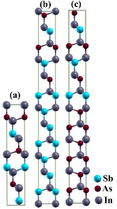
The atomic arrangement in a unit cell of CuPt ordered InSb0.5As0.5 is shown in Fig. 1 (a). The atomic arrangement in optimized HS unit cells of H-I with n=2 and H-II with m=3 are shown in Fig. 1 (b) and (c). The optimized structures of other HSs, i.e. with =1,3 (in H-I) and =1,2 (in H-II) are also obtained. A unit cell of CuPt ordered InSb0.5As0.5 has 12 layers of atoms. A unit cell of a ZB-InSb [111] has six layers of atom; whereas, the same for a WZ structure in [0001] direction has four layers of atomic arrangement. Thus, the number of layers in H-I are 18 (n=1), 24 (n=2) and 30 (n=3) whereas in H-II, the values are 16 (m=1), 20 (m=2) and 24 (m=3). The optimized lattice constant for CuPt ordered InSb0.5As0.5 are Å and Å with the space group (no. 160). Both H-I and H-II take a trigonal structure with the space group (no. 156). The lattice parameters of H-I (n=1–3) and H-II (m=1–3) are listed in Table-1.
| HS | a | c | |||
|---|---|---|---|---|---|
| in Å | in Å | ||||
| n | |||||
| 1 | 4.6077 | 33.8598 | |||
| H-I | 2 | 4.6154 | 45.2216 | ||
| 3 | 4.6231 | 56.6206 | |||
| m | |||||
| 1 | 4.4935 | 29.3514 | |||
| H-II | 2 | 4.4636 | 36.4449 | ||
| 3 | 4.3752 | 43.9056 |
III.2 Electronic properties
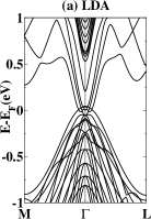
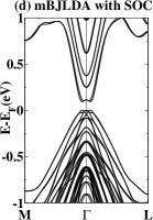
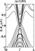
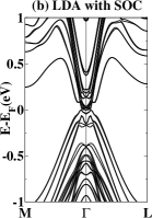
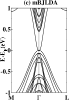
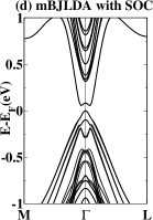
We have carried out systemic band structure calculations on two HSs, H-I and H-II with (n,m=1–3), using LDA, LDA with SOC, mBJLDA and mBJLDA with SOC schemes to demonsrate the role of the mBJLDA exchange potential and SOC in the band structure. From the calculated band structure, we plot the energy bands along -- k-paths. Fig. 2 (a)–(d) present the same for H-I (n=2). The standard LDA method yields this system as a gapless material (Fig. 2 (a)), However, the implementation of SOC interaction over LDA does not open a gap in the system (Fig. 2 (b)). The mBJLDA exchange potential creates a separation between the bands, present near the EF (see Fig. 2 (c)). Nonetheless, the band structure still exhibits metallic behavior. Incorporation of SOC over the mBJLDA calculation, as shown in Fig. 2 (d), shows a band gap. Similarly, for H-I with =1,3, the band gap could be obtained only using mBJLDA exchange potential with SOC. Above mentioned other calculation schemes showed the metallic behavior of the systems.
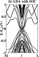
We have performed the calculations on H-II, with =1–3, following the same four-steps procedure as used for H-I. H-II (with =1–3) exhibited the same trend, as observed in the case of H-I. Under LDA, LDA with SOC and mBJLDA schemes, we obtained metallic behavior of this system. Incorporation of SOC over mBJ corrected LDA calculation opens a gap at the point. In Fig. 3 (a)–(d) we plot the energy bands of H-II with =3, as obtained using above the mentioned schemes.
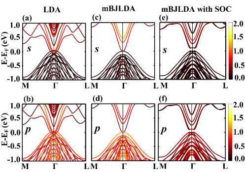
We note that the LDA underestimates the separation between different bands to a great extent. It is to be noted that for InSb based materials Sb-p states dominate near Cardona1 . Fat band analysis provides the contribution of atomic orbitals in the band structure. Fat bands showing the contribution of and orbitals in the band structure of H-I with n=2 under the LDA scheme are plotted in Fig. 4 (a)–(b), mBJLDA in Fig. 4 (c)–(d) and under mBJLDA+SOC in Fig. 4 (e)–(f). While the upper three panels, (a), (c) and (e), reveal the contribution of orbitals, the lower three panels (b), (d) and (d), demonstrate the contribution of the orbitals. We find that under LDA, In/As s and Sb p-orbitals mostly contribute near . The spin-orbit interaction becomes significant for high Z elements, like Sb. Incorporation of SOC in the calculation splits the bands and make the band structure more densely packed. However, this does not remove the contribution from the s-states, and it does not open the band gap. Since the mBJ potential corrects the conventional LDA Kim1 type of exchange correlations by considering the effect of holes, it creates the proper separation between the levels near EF Tran1 . The mBJLDA exchange potential separates the s-like states from the p-states near EF (see Fig. 4 (c)–(d)), which were wrongly mixed up at the LDA level. Under this scheme the Sb-p states dominate near , as expected Cardona1 . When SOC is included over the mBJLDA corrected bands, it provides the necessary symmetry breaking at the point, which in turn leads to a correct band structure (Fig. 4 (e)–(f)). We could apply the above arguments to explain the role of mBJLDA exchange potential and SOC in determining correct electronic band structure of other systems under study.
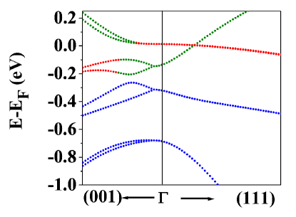
The band structure of InSb0.5As0.5 with CuPt ordering, calculated using mBJLDA potential, with SOC is shown in Fig. 5. We obtain stated Winkler1 topological features like band inversion at the level and the existence of the triple point. A novel topological phase is observed in this system through appearance of the triple point in the band structure. Our calculated band structure is an excellent match with that reported using HSEO6 Winkler1 . Here also we find that mBJLDA+SOC scheme is reliable to obtain details of electronic band structure.
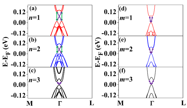
Next we take a close look at band structures near point for HSs under study. Refer to Fig. 6 (a)–(c) for H-I with n=1–3. In the figure the direct and indirect band to band transitions are shown by green and violet lines, respectively. For H-I with n=1,2 four transitions, two direct (shown by green) and two indirect (shown by violet lines) transitions are possible. All direct and indirect gaps are equal. The obtained values of the gaps are 0.143 eV and 0.115 eV for H-I with n=1 and =2, respectively. However, the band structure gets modified as the InSb layer thickness is further increased to . It has two indirect band gaps of same energy, 0.54 eV. On the contrary, no qualitative change in the nature of the band structure was observed as we vary the InAs layer thickness in H-II (Fig. 6 (d)–(f)). The systems, with m=1–3, exhibit two indirect band gaps of equal energy. Table-2 lists the gap energies (Egs) of the HSs. H-I shows a decrease of the gap from 0.143 to 0.054 eV for 1–3. However, for H-II with =1–3 the band gap changes only from 0.075 to 0.084 eV. The variation in band gap is an order of magnitude higher in H-I than in H-II with increase in the thickness of the layers.
| HS | Eg | hole | electron | ||
|---|---|---|---|---|---|
| in eV | pockets | pockets | |||
| n | |||||
| 1 | 0.143 | 6 | 1 | ||
| H-I | 2 | 0.115 | 7 | 6 | |
| 3 | 0.054 | 1 | - | ||
| m | |||||
| 1 | 0.075 | 1 | - | ||
| H-II | 2 | 0.074 | 1 | - | |
| 3 | 0.084 | 1 | - |
Doping or external field is often used to shift the EF in a system Zhu1 ; Yuan1 ; Song1 . A close inspection of the band structures of both HSs near the point reveals that a small shift in EF is expected to generate different number of Fermi pockets. A positive effective mass defines an electron pocket while a hole pocket has a negative effective mass. The curvature of the bands define the effective mass either to be positive or to be negative. Refer to Table-2. With a shift in EF, six hole pockets (three along equivalent - and similarly three along - direction) can be obtained in the band structure of H-I with =1. In addition, we find the possibility of having an electron pocket only at the point. With increase in the layer thickness, i.e. for 2 the number of hole and electron pockets increased to seven and six respectively. However, the number of carrier pockets reduced to one for =3. With a shift in , the band structure of H-II with =1–3 (see Fig. 6 (d)–(f)) is expected to exhibit only one hole pocket. Thus, we demonstrate that by varying the InSb layer thickness, one can engineer different carrier pockets (CPs) in H-I. CPs at a low symmetry points are enhances material functionality. For example, materials with large numbers of CPs are ideal for thermoelectric devices Rabin1 ; Zhou1 .
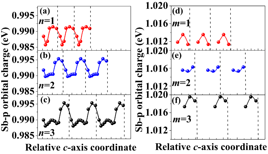
In above we observe that the intricate features of electronic band structures of H-I and H-II are markedly different. To find the possible origin of this difference in evolution characteristic of the electronic band structures of H-I and H-II with layer thickness, we looked into the charge modulation along the axis of the HSs. As seen through the fat band analysis, Sb p-orbitals of these systems have a dominant contribution near . We studied the variation of charge on Sb sites along the axis, as shown in Fig. 7 (a)–(c) and (d)–(f) for H-I and H-II respectively. In H-I, as we change the InSb layer thickness, the number of Sb atoms increases from six to twelve and they are inequivalent (see Fig. 7 (a)-(c)). Thus, the increase in InSb layer thickness in H-I has two consequences. First it shrinks the BZ along the Z-direction and secondly, it increases the number of states within the BZ (due to increase in inequivalent Sb atoms). As a consequence, the band structure significantly changes when changes from 1 to 3. In H-II, with an increase in the InAs layer thickness, the BZ shrinks. However, the numbers of relevant inequivalent atoms remain three for =1–3 (see Fig. 7 (d)–(f)). Hence, we do not find appreciable change in the band structure for this system.
IV Conclusion
In summary, we have calculated electronic band structure of two different HSs, one component of which is a topological semimetal of CuPt ordered InSb0.5As0.5 and other component is a band insulator. The HSs are also semiconductors. We have shown that for InSb/InAs0.5Sb0.5 HS, the band gap as well as fine features near the Fermi level can be modulated by varying the thickness of the InSb segment. Another important take away from this work is how differently these HSs would respond to a small perturbation owing to the difference in the number of their Fermi pockets.
Acknowledgements
Authors thank Professor Debraj Choudhury, IIT Kharagpur, for
valuable discussion. Authors also acknowledge the use of the
computing facility from the DST-Fund for Improvement of S&T
infrastructure ( phase-II) Project installed in the Department of
Physics, IIT Kharagpur, India. AR thanks Department of Science and
Technology, Government of India, for financial assistance.
References
- (1) A. Pitanti, D. Coquillat, D. Ercolani, L. Sorba, F. Teppe, W. Knap, G.De Simoni, F. Beltram, A. Tredicucci, M.S. Vitiello, Appl. Phys. Lett. 101 , 141103 (2012).
- (2) L. Höglund, D.Z. Ting, A. Khoshakhlagh, A. Soibel, C.J. Hill, A. Fisher, S. Keo, S.D. Gunapala, Appl. Phys. Lett. 103, 221908 (2013).
- (3) E. Steveler, M. Verdun, B. Portier, P. Chevalier, C. Dupuis, N. Bardou, J.-B. Rodriguez, R. Hal̈dar, F. Pardo, and J.-L. Pelouard, Appl. Phys. Lett. 105, 141103 (2014).
- (4) D. Jiang, X. Han, H. Hao, Y. Sun, Z. Jiang, Y. Lv, C. Guo, G. Wang, Y. Xu, Y. Yu, and Z. Niu, Appl. Phys. Lett. 111, 161101 (2017).
- (5) D. H. Wu, A. Dehzangi, Y. Y. Zhang, and M. Razeghi, Appl. Phys. Lett. 112, 241103 (2018).
- (6) T. Ashley, A. B. Dean, C. T. Elliott, G. J. Pryce, A. D. Johnson, and H. Willis, Appl. Phys. Lett. 66, 481 (1995).
- (7) M. J. L. Sourribes, I. Isakov, M. Panfilova, and P. A. Warburton, J. Appl. Phys. 121, 024304 (2017).
- (8) H.A. Nilsson, P. Caroff, C. Thelander, M. Larsson, J.B. Wagner, L.E. Wernersson, L. Samuelson and H. Q. Xu, Nano Lett. 9, 3151 (2009).
- (9) J. Johansson, K. A. Dick, P. Caroff, M. E. Messing, J. Bolinsson, K. Deppert, L. Samuelson J. Phys. Chem. C 114, 3837 (2010).
- (10) D. Ercolani, M. Gemmi, L. Nasi, F. Rossi, M. Pea, A. Li, G. Salviati, F. Beltram, and L. Sorba, Nanotechnology 23, 115606 (2012).
- (11) D. Singh, and L. Nordstrom, Planewaves, Pseudopotentials, and the LAPW Method (Springer, Berlin, 1994).
- (12) S. Blügel, and G. Bihlmayer, in Computational Nanoscience:, edited by J. Grotendorst, S. Blügel, and D. Marx, John von Neumann Institute for Computing NIC Series Vol. 31 (John von Neumann Institute for Computing, Jülich, 2006), p. 85.
- (13) P. Blaha, K. Schwarz, G. Madsen, D. Kvasnicka, and J. Luitz, WIEN2K, An Augmented Plane Wave plus Local Orbitals Program for Calculating Crystal Properties (Vienna University of Technology, Vienna, 2001).
- (14) A. Patra, M. Chakraborty, and A. Roy, Nanoscale 8, 18143 (2016).
- (15) F. Tran, and P. Blaha, Phys. Rev. Lett. 102, 226401 (2009).
- (16) P. E. Blöchl, O. Jepsen, and O. K. Andersen, Phys. Rev. B 49 ,16223 (1994).
- (17) M. Cardona, N. E. Christensen, and G. Fasol, Phys. Rev. 38, 1806 (1988).
- (18) Y.S. Kim, M. Marsman, G. Kresse, F. Tran and, P. Blaha, Phys. Rev. B 82, 205212 (2010).
- (19) G. W. Winkler, Q. Wu, M. Troyer, P. Krogstrup, and A. A. Soluyanov, Phys. Rev. Lett. 117, 076403 (2016).
- (20) Z. Y. Zhu, Y. C. Cheng, and U. Schwingenschlögl, Phys. Rev. B 84, 153402 (2011).
- (21) H. Yuan, M. S. Bahramy, K. Morimoto, S. Wu, K. Nomura, B. J. Yang, H. Shimotani, R. Suzuki, M. Toh, Ch. Kloc, X. Xu, R. Arita, N. Nagaosa, and Y. Iwasa, Nat. Phys. 9, 563 (2013).
- (22) Y. Song, X. Wang, and W. Mi, Npj Quantum Mater. 2, 15 (2017).
- (23) O. Rabin, Y.-M. Lin, and M. S. Dresselhaus, Appl. Phys. Lett. 79, 81 (2001).
- (24) Y. Zhou, and L.D. Zhao, Adv. Mater. 29, 1702676 (2017).