Influence of image forces on the interlayer exchange interaction in magnetic tunnel junctions with ferroelectric barrier
Abstract
We study interlayer exchange interaction in magnetic tunnel junctions with ferroelectric barrier. We focus on the influence of image forces on the voltage dependence of the interlayer magnetic interaction (magneto-electric effect). The influence of the image forces is twofold: 1) they significantly enforce magneto-electric effect occurring due to the surface charges at the interface between ferroelectric and ferromagnets; 2) in combination with voltage dependent dielectric constant of the ferroelectric barrier image forces cause an additional contribution to the magneto-electric effect in magnetic tunnel junctions. This contribution can exceed the one coming from surface charges. We compare the interlayer exchange coupling voltage variation with spin transfer torque effect and show that for half-metallic electrodes the interlayer exchange coupling variation is dominant and defines the magnetic state and dynamics of magnetization in the tunnel junction.
pacs:
75.50.Tt 75.75.Lf 75.30.Et 75.75.-cI Introduction
Interlayer exchange coupling (IEC) in magnetic tunnel junction (MTJ) is the long standing problem in the field of spintronics [Slonczewski, 1989; Carrera et al., 2016; Oh et al., 2009; Kubota et al., 2008; Sankey et al., 2008; Faure-Vincent et al., 2002; Bruno, 1995; Popova et al., 2006; Petit et al., 2007; Slonczewski, 2005; Katayama et al., 2006; Wu et al., 2009; Mavropoulos et al., 2005; Hammerling et al., 2003]. IEC is the interaction between magnetic moments of MTJ electrodes. It is described as the surface energy term of the form , where are the magnetizations of ferromagnetic (FM) leads (see Fig. 1) and is the coupling constant. The coupling induces an effective magnetic field acting on FM layers in MTJ, , with being the thickness of -th layer. This field may exceed coercive fields of the magnetic leads [Katayama et al., 2006; Popova et al., 2006; Faure-Vincent et al., 2002]. Thus, the IEC effect is of crucial importance for MTJ magnetic state. Moreover, it is shown theoretically and experimentally that IEC effect can be controlled with voltage () applied to MTJ [Xiao et al., 2008; Tang et al., 2009; Petit et al., 2007; Skowronski et al., 2013; Oh et al., 2009; Kubota et al., 2008; Sankey et al., 2008]. This opens an avenue to the voltage-based magnetization switching in MTJ, which is the crucial issue for magnetic memory applications. Note that IEC voltage dependence can be considered as magneto-electric (ME) effect [Eerenstein et al., 2006].
Applying voltage to MTJ results in a charge current which is spin polarized due to FM nature of electrodes. Such a current causes the so-called spin transfer torque (STT) effect [Slonczewski, 1989; Stiles and Zangwill, 2002], which is actively studied at now [Xiao et al., 2008; Tang et al., 2009; Petit et al., 2007; Skowronski et al., 2013; Oh et al., 2009; Kubota et al., 2008; Sankey et al., 2008]. STT effect leads to dynamics of magnetization and can be used to control MTJ magnetic state. However, switching of magnetization in MTJ with STT effect appears only at huge currents overheating the system. Another issue is the dynamical nature of STT based magnetization switching requiring sophisticated tuning of voltage pulse.
The IEC effect is not caused by electrical current flowing across the MTJ and exists even at zero voltage. In contrast, the STT effect is directly related to the electron flow between electrodes of the tunnel junction (TJ) and may not be associated with any energy term. This is a fundamental difference between IEC and STT effects. Spin transfer torque enters the macroscopic equation for magnetization dynamics as an additional dissipation term of the form , where is the strength of the STT effect, and is the gyromagnetic ratio.
In symmetric MTJ with the same FM metal in both electrodes the IEC effect is the even function of voltage, [Tang et al., 2009; Wilczynski et al., 2008; Chshiev et al., 2008; Theodonis et al., 2006; Xiao et al., 2008]. However, from practical point of view the odd voltage dependence of the IEC is more useful. It would allow one to change the magnetic coupling type from FM to antiferromagnetic (AFM) and finally to realize controllable reversible magnetization switching in MTJ avoiding problems of dynamical SST-based remagnetization.
Theoretically it is shown that the odd contribution to may appear for asymmetric MTJ (having different leads) [Tang et al., 2009]. IEC effect appears due to virtual hopping of electrons between FM leads and therefore is defined by the tunneling matrix. MTJ with different electrodes has asymmetric barrier resulting in the odd in voltage contribution to the tunneling probability. Weak odd contribution can also appear in the system with FM leads of different thickness [Heiliger and Stiles, 2008]. Recently, the IEC was considered in asymmetric MTJ with ferroelectric (FE) barrier [Zhuravlev et al., 2010]. Following Ref. [Dai, 2016] we will call such systems multiferroic tunnel junctions (MFTJ). In MFTJ the magnitude of IEC effect is defined by the direction of FE polarization. Switching of polarization direction changes the IEC strength. The dependence of the IEC effect on the polarization appears due to surface charges at the FE/FM interfaces in MTJ. They deform the barrier potential profile and therefore change tunneling matrix elements defining the IEC strength. These theoretical findings were not verified experimentally. IEC was studied mostly in symmetric MTJs without FE (such as Fe/MgO/Fe).
New mechanism of IEC was recently proposed for MFTJ and granular multiferroics [Udalov and Beloborodov, 2017a, b, c; Udalov et al., 2015a, b]. The IEC may appear due to the spin-dependent part of the s-s electron Coulomb interaction. Two electrons in different leads experience the Coulomb based exchange interaction as in the Heitler-London model. Summation of the interaction over all electron pairs gives the magnetic coupling between leads. In the case of granular system the Coulomb blockade affects the IEC and also depends on dielectric constant. Interestingly, the IEC due to the many-body effects is inversely proportional to the FE barrier dielectric constant, . In its turn is voltage dependent in FEs and has the odd in voltage contribution leading to the odd component of the IEC effect in MFTJ.
In the present paper we will study one more mechanism leading to odd contribution in IEC voltage dependence in MFTJ. In contrast to our previous works [Udalov and Beloborodov, 2017a, b, c; Udalov et al., 2015a, b], here we do not take into account the exchange interaction between s-s electrons and the Coulomb blockade. We focus on the hopping based IEC effect taking into account image forces acting on electrons in the barrier. Image forces were neglected in previous studies of IEC effect. This is reasonable for MTJ without FE barrier since in this case the forces just reduce the barrier height independently of applied voltage. This is not the case in MFTJ. Image forces are inversely proportional to the barrier dielectric constant, . Since is voltage dependent in FEs, the barrier reduction due to the image forces is also voltage dependent. This introduces an additional odd contribution to dependence in MFTJ.
Recently, influence of image forces on electron transport in non-magnetic TJ with FE barrier and in granular metal with FE matrix was studied [Udalov et al., 2014a, b; Udalov and Beloborodov, 2017d]. In the case of granular FE the image forces affect the Coulomb blockade effect leading to conductivity modification. In FE tunnel junctions the image forces essentially influence electron transport and cause significant electro-resistance effect. In the present manuscript we add magnetic degrees of freedom and study thermodynamic rather than transport properties of TJ.
The goals of this work are the following: 1) study the influence of image forces on the IEC effect due to surface charges created by the FE polarization, Ref. [Zhuravlev et al., 2010]; 2) investigate the ME effect appearing due to combination of image forces and voltage dependent dielectric constant of the FE barrier; 3) compare IEC voltage variation with STT effect.
TJ with FE barrier is currently not very well studied. Thin FE films lose their electrical properties as their thickness is reduced down to the nm scale range [Fridkin, 2006]. Therefore, the fabrication technique for TJ with FE barrier is rather complicated. A lot of efforts were spent to investigate transport properties of non-magnetic TJ with FE barrier [Tsymbal and Gruverman, 2013]. The magneto-resistance effect in MFTJ was also studied [Yin et al., 2011]. Investigation of IEC effect in MFTJ is just started recently [Carrera et al., 2016].
The paper is organized as follows. The model of MTJ with FE barrier and calculations of IEC and STT effects are given in Sec. II. In Sec. III subsections A and B we discuss general behavior of IEC and STT effects. Dependencies of IEC and STT effects on various parameters are discussed in subsections C-H of Sec. III. Last subsection of Sec. III is devoted to magnetization switching based on the IEC effect in MFTJ.
II The model
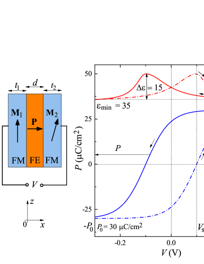
In order to study the IEC in MFTJ we will use the following simple model. We assume that conduction electrons are responsible for the interlayer interaction. MFTJ consists of two homogeneously magnetized FM layers and FE insulating spacer. Electrodes are thick enough and can be considered as infinite. A voltage is applied to the MFTJ. The FE barrier has polarization , dielectric constant and thickness (see Fig. 1). Polarization is uniform and directed along the x-axis. Both polarization and dielectric constant are functions of the applied voltage (see details in Sec. II.1). The Hamiltonian for electrons is given by
| (1) |
where unit vectors are directed along magnetizations of the leads, is the vector of Pauli matrices, is the spin subband splitting occurring due to interaction of conduction electrons with localized ones (as in Vonsovskii s-d model) or due to exchange interaction between conduction electrons themselves [Vonsovskii, 1974], is the coordinate perpendicular to the layers surfaces, and are the effective electron masses in metallic leads and the insulator layer. Generally the effective mass in FM leads may be spin dependent, especially in half-metals, but we do not take this into account for simplicity. defines the barrier height above the Fermi level of the left lead. We assume that the Fermi level of the left electrode corresponds to zero energy. The right lead is biased by the applied voltage. Quantities determine the bottoms of the conduction majority and minority spin bands. Using these quantities one can define the minority and majority Fermi momentums, . If both minority and majority bands exist and we have two band ferromagnet (TBF). If , only one spin subband works and the leads are half-metal ferromagnets (HMF). The potential appears due to the influence of the FE polarization and is defined as follows [Zhuravlev et al., 2005a]
| (2) |
with the characteristic potential created by surface charges
| (3) |
Here is the electron charge, is the vacuum dielectric constant, is the Thomas-Fermi screening length. The potentials are found using electrostatic problem where FE with polarization is clamped in between two metals. The metals are treated within the Thomas-Fermi approximation with close circuit conditions.
The term in Eq. (1) describes the influence of the image forces. They appear due to the interaction of electron inside the barrier and image charges occurring in metallic leads. We assume that electron concentration in the leads is high enough and the screening length in these metals is small enough (). In this case one can use a simple picture of image forces inside the insulating barrier [Burstein and Lundqvist, 1969]
| (4) |
The terms with voltage in Eq. (1) describe the effect of the applied voltage. Following Refs. [Burstein and Lundqvist, 1969,Zhuravlev et al., 2005a] we introduce the total potential barrier “seen” by tunneling electron as follows (region )
| (5) |
Calculating the image forces potential we treat the metallic leads as ideal neglecting corrections due to finite screening length. When calculating potentials the finite screening length is crucial and can not be neglected. Note that diverges at points and . In fact, in the vicinity of these points the image forces approximation does not work. The region where potential is not valid is defined by the size of the correlation hole size in metal. Usually it is of order of 0.05 nm. In this region the potential should smoothly transform from to the bulk metal potential. Since we consider FM lead the potential in the vicinity of metal/insulator interface should be spin dependent even inside the insulator. In our calculations we restricted image force potential at the level of the lower spin subband bottom. We tried a number of image forces potential shapes. All shapes give the same result, due to the fact that the shape of image forces potential in the close proximity to FM/FE interface influences only the low lying electron states. These electrons make small contribution to the overall IEC effect. The true potential profile in the vicinity of the interface is a long standing problem which is not fully resolved by now. Even ab initio calculations based on density functional theory do not provide an acceptable picture of the potential profile.
II.1 FE layer
FE polarization below the Curie temperature is a function of applied voltage and has a hysteresis. We use the following formula to describe the FE polarization as a function of applied voltage
| (6) |
where is the switching voltage, is the saturation polarization, is the width of the transition region. Superscripts “” and “” correspond to the upper and the lower hysteresis branch, respectively. For example, the polarization of HfZrO2 is shown in Fig. 1 and can be approximately described with the following parameters: C/cm2, V (with being measured in m), and . The parameters were obtained by fitting the experimental curves of Ref. [Muller et al., 2012].
The dependence of dielectric constant on voltage is given by the expression
| (7) |
This dependence captures the basic features of dielectric constant behavior as a function of electric field. The dielectric permittivity has two branches corresponding to two polarization states. In the vicinity of the switching bias the dielectric permittivity, has a peak. For example, the dielectric constant of HfZrO2 can be described using the following parameters: , (see Fig. 1).
II.2 Toy model of the electron potential profile
On one hand the potential profile given in Eq. (5) is complicated enough and does not allow for analytical solution of Shrodinger equation and calculating of wave functions. On the other hand the profile does not take into account several phenomena such as band structure of leads and the barrier, exchange-correlation effects in the vicinity of the FM/I interface. Since it does not allow making quantitative estimates of the IEC in MTJ we will further simplify the potential profile. Our simplification will not reduce the quantitative precision of our calculations but still capture the main physical phenomena that we will study in the present work.
The effect of the surface charges potential on IEC is studied in Ref. [Zhuravlev et al., 2005b]. Surface charges change the potential barrier for electrons and therefore change the tunneling probability. This effect can be captured within the quasiclassical approximation in which the average barrier height defines the tunneling probability. The influence of image force on the total barrier profile is twofold: 1) decreasing of the effective barrier width; and 2) decreasing of the effective barrier height. Generally, these two effects are also captured by the quasiclassical approximation.
We will change the initial barrier in Eq. (5) with effective rectangular barrier of width and height . Within the quasiclassical approximation the effective barrier thickness is defined by the intersection of the potential profile with the electron energy level. The points of intersection are and . This point generally depends on the electron energy.
Note that due to the bias applied to the MFTJ the Fermi levels are different in the left and the right leads and the effective barrier “seen” by electrons in the right and the left electrodes is different. Generally, we can introduce a different barrier thickness for electrons in different leads . To determine we find the intersection (points ) of with electron energy. To determine we find intersections (points ) of with energy which is the Fermi level of the right lead). At zero bias .
If we neglect the image forces the effective barrier thickness is the same for electrons in both leads and at any energy is equal to . In the opposite situation when we neglect the effect of the bias and polarization the effective thickness at Fermi level is given by . The quantity is given by
| (8) |
This is the characteristic potential associated with image forces in TJ. Particularly, is the reduction of the initial potential barrier height (see Eq. (5)) at the symmetry point () at zero bias.
Effective barrier height “seen” by electrons in different leads is also different and one can introduce . Even in the absence of the image forces and surface charges the applied bias leads to difference in the height of and . A general expression for the effective barrier height has the form
| (9) |
Here is the electron energy counted from the Fermi level of the left electrode. Since due to the bias occupied electron energies are different in the left and the right lead one has different effective barriers.
In the next two subsections we provide simplified expressions for IEC and STT in MTJ. In these formulas we take into account only the electrons at the Fermi level and use for effective barrier heights for electrons in the left and the right leads at their Fermi levels. While this approach is oversimplified and misses some important phenomena it still gives general trends of IEC and STT effect which is useful to keep in mind. In Sec. III we calculate IEC and STT effects taking into account all electrons at all energy levels (see Appendix A).
The most important phenomena that we study is the dependence of the IEC on dielectric properties of the barrier. The higher the dielectric constant the weaker the influence of image forces. For infinite the image force potential disappears. This effect is captured in the toy potential. Similarly, the influence of voltage and FE polarization is also captured in this approach.
II.3 Exchange interaction in MTJ
Interlayer exchange coupling in MTJ can be described using the following macroscopic surface energy density, . IEC effect enters in to the Landau-Lifshitz-Gilber (LLG) equation as the torque, . We will follow Slonczewski approach to calculate the IEC in MFTJ. The IEC is given by the equation
| (10) |
where is the y spin component of the spin current density carried by the electron in the state . The sum is over all orbital and spin states in both leads. Orbital state is described by quasimomentum inside each lead. Spin quantization axis for electrons in left (right) lead is along magnetization of left (right) electrode. To calculate spin current of an electron in the state we find an electron wave function using the effective rectangular barrier model. We calculate the effective barrier height and width for each state (see more details in the Appendix A). The magnitude of the spin current depends on the mutual orientation of and as , where is the angle between and . We calculate spin currents at .
Simplified analytical expressions for IEC in MFTJ can be found following Slonczewski approach [Slonczewski, 1989]
| (11) |
where
| (12) |
Here we use the electron wave function inverse decay lengths, . The effective barrier parameters should be calculated at the Fermi levels of the left and the right electrodes, correspondingly. For zero voltage, , and the above expression turns into Slonczewski formula. At finite bias the electron tunneling from the left electrode to the right one “sees” a different barrier comparing to electron moving in the opposite direction. This results in voltage dependence of IEC effect.
II.4 Spin transfer torque
The STT appears at finite bias [Slonczewski, 1989]. This effect is described by a tensor with spin and orbital indexes. In our case the electron current flows along the x-axis. The tensor elements with orbital indexes and are zero. Therefore, we omit the orbital index in the spin current notation and keep only the spin index. The STT effect can not be associated with some energy contribution as the IEC effect [Slonczewski, 2005]. It can be introduced into LLG equation for leads magnetizations as an additional torque in the form, . Note that the magnitude of the torques acting on the left and the right leads can be different at finite voltage. System symmetry results in the following relation, . Below we will calculate the STT acting on the left lead and will omit the upper index. The STT effect does not exist without a charge current and is always related to energy dissipations. Therefore, we mark it with the subscript “”.
STT has angular dependence similar to IEC, . For clarity we assume that is along z-axis. Then, the x-component of spin current flowing into the left lead is associated with STT effect. We neglect the z-component of the spin current when calculating the STT acting on the left lead. This is reasonable providing that the magnitude of magnetization is fixed by strong internal interaction. The STT effect constant is given by the following expression
| (13) |
where summation is only over electrons carrying the electric current (see Appendix A for details).
For analytical analysis one can use the simplified expression [Slonczewski, 1989]
| (14) |
where the quantity is given by
| (15) |
The effective barrier parameter are calculated at the Fermi level of the left (right) lead for positive (negative) . Equation (14) provides the linear in voltage term to the STT only. Therefore, it can not describe the STT voltage asymmetry known theoretically and experimentally [Theodonis et al., 2006; Xiao et al., 2008; Oh et al., 2009; Kubota et al., 2008; Sankey et al., 2008]. In our numerical calculations we take this effect into account.
III Exchange interaction in MFTJ
In this section we will calculate the IEC and STT in MFTJ as a function of applied voltage depending on the system parameters.
Voltage dependence of IEC can be considered as ME effect in MFTJ. In the literature a variation of the IEC constant with voltage is called field-like (or perpendicular) STT effect [Xiao et al., 2008; Oh et al., 2009; Kubota et al., 2008; Sankey et al., 2008]. We will refer the IEC variation as the ME effect in the present work.
Variation of may cause a variation of the system magnetic state. Similarly, STT may also cause magnetization rotation. STT and IEC effects produce spin currents flowing across the tunnel junction. The spin direction of these currents is different. The IEC produces the spin current perpendicular to magnetization plane while the STT causes the spin current in the plane of system magnetization. We will compare here only magnitudes of these spin currents and . Magnetization dynamics in MFTJ under the action of IEC variation and the STT effect is beyond the scope of the present manuscript and requires a separate investigation.
III.1 System parameters
Generally, the system has a lot of parameters. To reduce the number of variables we fixed some of them. We will use the parameters value chosen in this section in all cases below.
On one hand the FE can not be thinner than a single atomic layer, on the other hand the IEC itself decreases exponentially with for nm [Katayama et al., 2006; Popova et al., 2006; Faure-Vincent et al., 2002]. So, we will use nm in all our calculations keeping in mind that only for such a thin barrier the IEC has some impact on the magnetic state of MTJ.
In a similar way we will fix the barrier height eV in all our calculations. Such a value is relevant for FE insulators. Obviously, increasing the height decreases the exchange interaction between the leads and the STT effect. Therefore, it is better to keep it as small as possible to be able to influence the magnetic state of MFTJ.
Also we fix parameters of the FE polarization hysteresis loop such as switching voltage, V and the switching transition region, V. They correspond to 1 nm thick layer of Hf0.5Zr0.5O2 (see experimental data of Ref. [Muller et al., 2012]).
We fix the effective mass in the barrier, at the level of 0.4 electron mass. It follows from Eq. (11) that the IEC effect decreases with the barrier effective mass growth. In the absence of polarization and image forces the following relation holds . The STT effect decreases slower than the IEC with the growth of barrier effective mass, , see Eq. (14).
Similar scaling rules can be written for effective mass of electron in FM leads, and . In all calculations we use of electron mass.
III.2 General remarks
In this section we use Eqs. (5), (11) and (14) to analyze general properties of IEC and STT effects.
1) Since we consider the symmetric MTJ the IEC effect does not depend on the direction of FE polarization at zero bias voltage. Spin transfer torque is absent at .
2) The IEC depends on while the STT depends on . This immediately leads to the fact that the STT becomes more important with decreasing of .
3) At zero polarization due to the system symmetry the IEC effect should be an even function of voltage. Neglecting the image charges one can get
| (16) |
The linear term does not contribute to the IEC effect (which follows from the symmetry consideration). The quadratic term shows that effective barrier reduces with increasing voltage. Thus, the IEC effect increases with voltage in agreement with other calculations [Theodonis et al., 2006].
4) Neglecting the surface charges () and at one gets the following expression for the average barrier height at the Fermi level
| (17) |
One can see that the higher the higher the barrier and the smaller and . This is the most general effect of the image forces.
Note that many FEs (for example BTO or PZT) have very high dielectric constants () making image forces negligibly weak. Image forces are significant in FEs with low dielectric constant only. There are a number of low dielectric constant FEs such as hafnium oxide family XHfO2 (where X can be Y, Co, Zr, Si) [Olsen et al., 2012; Park et al., 2014; Boscke et al., 2011], rare-earth manganites XMnO3 (where X is the rare-earth element) [Goto et al., 2004], colemanite [Fatuzzo, 1960], Li-doped ZnO [Wang et al., 2003], etc. There are also numerous organic FEs with low dielectric constant [Naber et al., 2010; Zhang and Xiong, 2012; Horiuchi and Tokura, 2008].
5) For voltage dependent dielectric constant the effective barrier height acquires an additional (to that shown in Eq. (16)) dependence on voltage. If has the odd component (as it does in FE), the barrier height and the IEC would also have the linear in voltage contribution caused by image forces.
6) At zero voltage and neglecting image forces one can get the following estimate for the effective barrier
| (18) |
Surface charges reduce the barrier at zero voltage and increases the IEC and STT effects. This reduction of barrier appears due to internal electric field created by the surface charges. This effect is similar to the one discussed in the third clause.
At finite voltage the electric fields produced by polarization and voltage can be co-directed or counter-directed. For example, for positive voltage and positive polarization both electric fields are co-directed leading to the reduction of the barrier height and to the increase of the IEC effect. Negative voltage at decreases the interlayer coupling. FE polarization (surface charges) breaks the MTJ symmetry and results in the linear contribution to the voltage dependence of the IEC effect.
III.3 IEC and STT as a function of spin subband splitting,
Figure 2 shows a typical dependence of IEC and STT on the spin subband splitting, , for the following parameters: eV, V (STT is finite only for non-zero voltage). We neglect here the FE polarization () but consider the image forces. We show the curves for several value of . The IEC is positive for small spin subband splitting and changes its sign for approaching . For HMF case () the IEC effect is negative. has a similar behavior, changing its sign for large spin subband splitting.
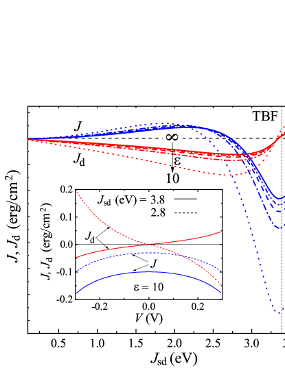
Note that spin subband splitting and Fermi energy can be tuned in many compounds varying proportions of material components. For example, the spin subband splitting in FM metal Co1-xFexS2 [Ramesha et al., 2004] strongly depends on concentration of Fe and Co. At zero Fe concentration the material is a TBF. Increasing of Fe concentration transforms this material to a half-metal.
STT is much weaker for MFTJ with half-metal electrodes (), comparing to the IEC constant . Thus, in HMF region the voltage based variation of IEC (ME effect) is the main option for the control of MFTJ magnetic state. For two band FM metals both the STT and IEC variation are important. For small enough spin subband splitting the STT becomes the most important mechanism causing MTJ magnetic dynamics under applied voltage.
Parameters and depend on dielectric constant of the barrier . Increasing increases the average barrier height according to our estimates, Eq. (17). This leads to decreasing of coupling and the STT effect. One can see that variation of with is significant and comparable to the value of the STT effect.
III.4 Dependence of the IEC and STT on voltage in MTJ without FE
Inset in Fig. 2 shows the IEC and STT effects as a function of applied voltage in MTJ with simple insulating barrier ( and is voltage independent). We use as in MgO barrier. Two curves for IEC correspond to different values of spin subband splitting, . It is known [Tang et al., 2009] that variation of IEC with applied voltage is comparable to the STT in MTJ. STT is asymmetric function (see red lines) of voltage in agreement with previous theoretical and experimental studies [Theodonis et al., 2006; Xiao et al., 2008; Oh et al., 2009; Kubota et al., 2008; Sankey et al., 2008]. Dependence of IEC on voltage is an even function of due to symmetry of the tunnel junction without FE barrier.
III.5 Influence of image forces and surface charges on the IEC in MFTJ
Both the surface charges (and associated potential ) and the image forces () influence the IEC effect in MTJ with FE barrier. To study their effect we calculate three different quantities , and . The first one, , is the IEC effect taking into account only image forces and neglecting the potential (we put but use the voltage-dependent in Eq. (7)). is calculated neglecting (image forces) but taking into account surface charges described by . Quantity accounts for both effects.
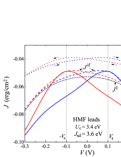
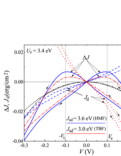
Figure 3 shows the IEC effect as a function of voltage for the case of HMF leads with eV and eV. These parameters correspond to HMF Co2MnSi [Galanakis et al., 2006; Sakuraba et al., 2006]. The HMF has a rather complicated band structure. We model it with free electron model. Majority and minority spin bands bottoms are taken from ab initio calculations. Effective mass is found by fitting the density of states at the Fermi level in the majority spin band to the density of states in ab initio calculations. The chosen effective mass ( of free electron mass) corresponds to HMF Co2MnSi. Note that this material demonstrates half-metallic properties and high tunneling magneto-resistance in MTJ structure [Sakuraba et al., 2006; Marukame et al., 2007] in contrast to many HMFs losing their high spin polarization at an interface [Katsnelson et al., 2008]. Curves in Fig. 3 correspond to FE barrier with saturation polarization C/cm2. Variation of dielectric constant in the barrier is described by Eq. (7) with and . These parameters correspond to Hf0.5Zr0.5O2 FE [Olsen et al., 2012].
Black short dashed line in Fig. 3 shows the IEC () as a function of voltage neglecting the dependence of polarization () and dielectric constant () on bias. Nevertheless the image forces are taken into account. This corresponds to the case of a simple insulator. The dependence is an even function of voltage. Variation of IEC with voltage is significant (about 25% in the shown voltage range). Increasing of IEC magnitude with voltage is caused by reducing of the effective barrier when bias voltage is applied (see Eq. (16)).
Dotted line in Fig. 3 shows the IEC in MFTJ neglecting image forces, . The exchange coupling as a function of voltage has two branches corresponding to two different FE polarization states, and . Arrows indicate the path of the hysteresis loop.
Two maxima at correspond to polarization switching. As we stated the electric fields induced by polarization and bias voltage can be either co-directed or counter-directed. Switching between these two situations happens at . This explains the occurrence of these two maxima.
At zero voltage the IEC has the same value for both branches due to the system symmetry. At finite voltage the symmetry is broken and the IEC depends on polarization state. At small voltages one can write, . This is in contrast to the situation considered in Ref. [Zhuravlev et al., 2005a] where MTJ with different magnetic leads show a different IEC effect at zero voltage for two different polarization states.
Note that even though the image forces are not taken into account when calculating the voltage dependence of dielectric constant, still influences the IEC. According to Eq. (2) the dielectric constant defines the potential barrier disturbance by the surface charges. The higher the lower the influence of surface charges. The influence of bias dependence on surface charge potential and on the tunneling electro-resistance and magneto-resistance was considered in Ref. [Zhang et al., 2012]. Similarly, contribute to the IEC variation in the present model.
Influence of the surface charges on the IEC effect does not exceed several percent which is less than IEC variation without FE barrier (black short dashed line).
Influence of image forces alone is shown with red and blue dashed lines, . Behavior of is similar to . It has two branches corresponding to two branches of dielectric constant and , Eq. (7). At zero bias the IEC is the same for both branches. According to our estimates (Eq. (17)) the increase of dielectric permittivity leads to the decrease of tunneling probability and therefore to the decrease of exchange coupling. The dielectric constant has maxima at . This explains two peaks of IEC at .
The change of IEC effect due to image forces alone is large than due to surface charges, but still not as large as changes caused by voltage itself. We estimate the IEC changes due to image forces as difference between IEC for the upper (or lower) branch at and at (). IEC variation due to voltage can be estimated as difference between at finite and at zero voltage (). One can see that at the quantity is larger than , but with increasing voltage exceeds the IEC changes due to image forces.
The situation changes drastically, when both image forces and surface charges are taken into account. Corresponding curves () are shown with red and blue solid lines in Fig. 3. The curves have similar shape as and , but have much larger variation. Moreover, the IEC has strong linear dependence at voltages , which may be useful for applications (see Sec. III.9). Thus, the curves demonstrate that image forces together with surface charges essentially change the dependence of the IEC effect on applied voltage in MFTJ.
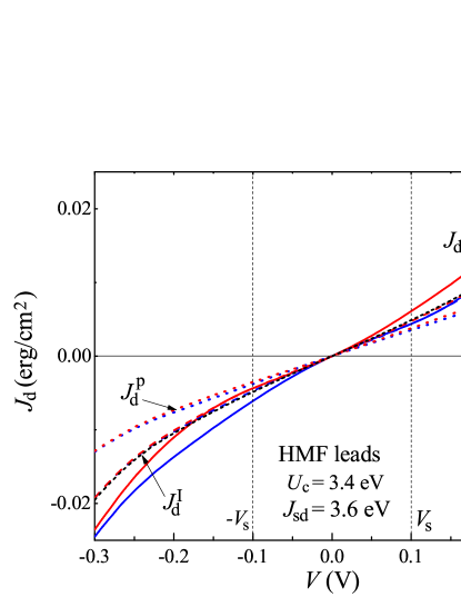
III.6 Influence of image forces and surface charges on STT in MFTJ
Image forces and surface charges influence the STT effect in MFTJ as well. However, their influence in this case is not very pronounced. Figure 5 shows the voltage dependence of the STT magnitude. The same parameters and notations are used as in the previous figure. Superscript “” means that the STT is calculated for MTJ with an insulator barrier ( and is voltage independent. Superscript “” stands for STT calculated in the presence of image forces and voltage dependent dielectric constant, but for . stands for STT effect accounting for surface charges in the absence of image forces. The STT in the presence of both effects is denoted with . Neither image forces nor surface charges qualitatively change the STT voltage behavior. However, a weak hysteresis appears when both effect are taken into account.
III.7 STT vs IEC in MFTJ
In this section we compare the magnitude of STT effect and variation of IEC effect with voltage (see Fig. 5). We subtract the IEC effect at zero voltage from the dependence introducing the notation, . Here we take both image forces and surface charges into account. Two cases are shown: (HMF case) and (TBF case). In the case of two band FM leads the STT effect grows fast with voltage and exceeds the IEC variation (compare red dotted and red dash dotted lines in Fig. 5). Thus, mostly the STT is responsible for magnetization dynamics in this case. In the case of HMF leads the IEC variation becomes stronger than the STT effect (compare blue dashed and blue solid lines in Fig. 5). In this case mainly the IEC defines the magnetization dynamics and even the magnetic state of MFTJ.
Black dash dot dotted and short dashed lines () shows the IEC variation in MTJ without FE barrier. Coupling changes caused by image forces and surface charges essentially exceed the ones caused by the voltage itself (), at least in the region of voltages below the FE switching ().
Thus, image forces and surface charges result in enforcement of IEC variation with voltage. Such variations become stronger than the STT effect in MFTJ with HMF leads. It is even more important that the image forces and surface charges produce the linear in voltage contribution to the IEC effect, which does not occur in symmetric MTJ without FE barrier.
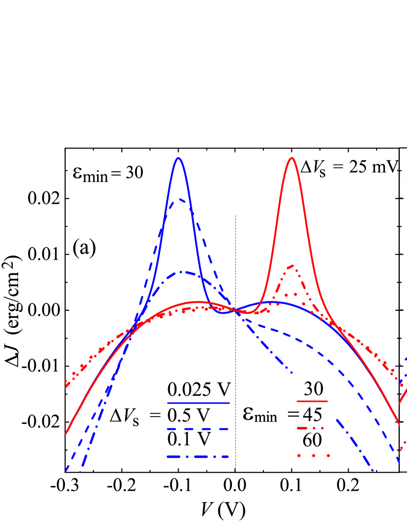
III.8 Variation of IEC as a function of barrier parameters
Figure 6 shows dependence of IEC variation on various barrier parameters. Here we calculate the IEC by taking into account both surface charges and image forces. Panel (a) shows as a function of minimum dielectric constant, and polarization switching region width, . Blue lines show for three different for fixed . These curves correspond to the upper branch of FE hysteresis loop. The dependence for lower branches is a mirror reflection with respect to zero voltage, . Red curves show for tree different at fixed V. Only lower hysteresis branches are shown. All curves are for the following parameters: V, , C/cm2, eV, eV.
The peak of IEC variation at grows with decreasing of the transition region width . This can be understood as follows. According to Eqs. (17) and (18) the decrease of dielectric constant decreases the effective barrier due to both surface charges and image forces. The decrease of transition region, leads to the reduction of at zero voltage (see Eq. (7)). The dielectric constant at stays the same, . Finally, the IEC effect grows at and stays the same at leading to peak growth.
Red curves show that the IEC variation strongly depends on the minimum dielectric constant, . Growth of leads to the decrease of IEC variation. The strength of image forces and potentials created by the surface charges are inversely proportional to the dielectric constant. Therefore, increasing of minimum value of reduces the effect of surface charges and image forces.
Panels (b) and (c) provide an additional insight into the effect of image forces on IEC. Both panels show for different values of saturation polarization, and variation of dielectric constant, . Blue (red) curves show modification of with varying of (). We use the following parameters: eV, eV and V. In panel (b) the curves correspond to the low barrier system with eV. In this case (see blue curves) influences the IEC effect much stronger than the (see red curves). We conclude that in this case the IEC variation appears due to modulation of FE polarization rather than due to the modulation of dielectric constant with voltage. However, image forces essentially enhance the effect of surface charges. Panel (b) shows the case of high barrier, eV. In this case situation is the opposite: curves weakly depend on polarization (see blue curves) and strongly depend on (see red curves). This means that the dependence of dielectric constant on voltage is the main source of the IEC variation (ME effect) and one can neglect the variation of polarization.
To conclude, the role of image forces is twofold: 1) they enhance the IEC variations caused by surface charges, even in the absence of voltage dependence of and 2) due to variation of dielectric constant with voltage the image forces cause the ME effect which can be even stronger than that caused by surface charges.
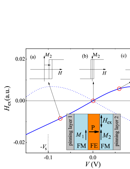
III.9 Magnetization switching in the MFTJ
Dependence of IEC on voltage can be used for switching of magnetization in MFTJ. Importantly, the switching mechanism is essentially different comparing to the STT effect. The STT effect may be used for dynamical switching only. It does not correspond to any energy contribution in the system Hamiltonian and can cause rotation of magnetization independently of magnetization state. In contrast, the IEC effect defines the system ground state. As it was shown above the interlayer coupling may have a linear contribution as a function of voltage. At zero voltage the IEC is finite. Consider the following system. The left FM layer is pinned (see Fig. 7) and can not be switched. At zero bias this layer produces an effective field acting on the right layer . The right layer has small enough coercive field and is pinned also. The second pinning layer is chosen such that it compensates the IEC effect at zero voltage. Pinning magnetic field acting on the right layer is . In this case the sign of the effective IEC (IEC effect + pinning) depends on voltage sign. Positive voltage would create the FM IEC while the negative voltage creates the AFM IEC. If coercive field of the right layer is smaller than the IEC variation, one can switch the magnetization with voltage. There is no need to tune voltage impulse parameters to get reliable switching, in contrast to STT based remagnetization. The IEC variation of erg/cm2 creates an effective field Oe acting on the material with saturation magnetization Gs and thickness nm. Therefore, if the material has a coercive field lower than 80 Oe, one can switch it with electric field.
For example, half-metal F3O4 has a rather small magnetization at room temperature about 140 Gs, meaning that the effective IEC field variation can be as high as 250 Oe which is the same as the coercive field of the material [Tang et al., 2001].
HMF considered in the present work Co2MnSi has the coercive field in the range of 10 to 100 Oe depending on fabrication conditions [Erb et al., 2010; Raphael et al., 2001]. Thus, it can be also switched with IEC variation effect.
IV Conclusion
We studied voltage dependence of the IEC and STT effects in MTJ with FE barrier. We took into account two phenomena influencing the IEC in MFTJ: 1) modification of the tunnel barrier potential due to the FE polarization; 2) modification of the barrier due to image forces acting on electrons in the tunneling spacer. Voltage dependent polarization results in the voltage dependent IEC effect. The influence of the image forces is twofold: i) they enhance the IEC variation occurring due to FE polarization and ii) image forces in combination with voltage dependent dielectric constant of the FE barrier produce an additional contribution to the interlayer coupling variation. This contribution becomes the dominant for MFTJ with high barrier. We compare the IEC with the STT effect occurring at finite voltage in MTJ. In the case of HMF the variation of IEC effect is the dominant mechanism defining MTJ magnetic state and dynamics. We estimate the variation of IEC effect and show that it can be used for controllable switching of magnetization in MFTJ with HMF leads.
V Acknowledgements
This research was supported by NSF under Cooperative Agreement Award EEC-1160504 and NSF PREM Award. O.U. was supported by Russian Science Foundation (Grant 16-12-10340).
Appendix A IEC and STT formulas
Consider two FM leads separated by a rectangular barrier of width (). Magnetizations of the leads are orthogonal. Left (right) lead magnetization is along the z(x)-axis. Consider a majority spin electron with unit incident flux in the left lead with energy moving to the barrier. The quasimomentum of up (or majority) band electron in the left lead is . For down (minority) spin band the quasimomentum is in the left lead. In the right lead the quasimomentum of up (down) spin electron with energy is (). Inside the barrier the electron wave function decays. The barrier potential is spin-independent. Therefore, the decay length, is spin-independent, however it is energy dependent. Lets calculate the spin current of a single electron inside the barrier. Spin current flows along the x-axis (across the barrier). We omit the spatial direction index in the notation of spin current and keep only the spin index. We consider several different cases depending on electron energy, bias voltage and spin subband splitting.
First consider the case when all , , and are real. In this case we have
| (19) |
| (20) |
| (21) |
These expressions coincide with Slonczewski formulas if one put and . The spin current for electron incident on the barrier from the left electrode with down spin can be found using the following relations , .
Note that here we use slightly different notations comparing to the main text (see Eq. (10)). The upper index here stands for spin state of an electron only, while in the main text the index was responsible for both spin and orbital states.
Now consider the case when only the majority spin states in both leads are allowed and the minority spin states can not propagate ( and are real, and are imaginary).
| (22) |
| (23) |
Minority (down) spin states do not propagate in this case and . This result agrees with Slonczewski result for one band leads (if one put and ).
However, at finite voltage (or in MTJ with different leads) the situations can occur when only one spin channel is “active” in one reservoir and two spin channels are available in the other. Consider the case when both spin bands are active in the left electrode and only one works in the right lead.
| (24) |
| (25) |
Expression for electron in minority spin band can be obtained with the substitutions , .
In the opposite case when only one spin band is “active” in the left electrode and two spin bands are available in the right electrode we have
| (26) |
| (27) |
| (28) |
The formulas are the same as for the two band case (considered first), but down spin electron are absent in the left lead in this case and .
The last case is related to the situation when there are no states in both spin bands in the right electrode. The right electrode behaves as an insulator in this energy region. In this case there is no electron flow across the barrier and . The y-component is not zero
| (29) |
| (30) |
Spin current created by an electron incident on the barrier from the right electrode can be found by the following relations . The sign “” occurs because the electron moves in the opposite direction in comparison to the electron in the left electrode. At the same time .
The IEC effect is related to the y-component of the spin current. To calculate the constant one has to sum the spin current over all spin and orbital states in both leads. To calculate the y-component of the spin current created by the left lead electrons we use the equation
| (31) |
To simplify formulas we omit the factor below. In the above equation we use in the following quasimomentums , , , . Spin current should be used with , , and . For each energy we calculate the effective barrier thickness and the inverse decay length, . The effective barrier thickness is defined by intersection of potential Eq. (5) with energy level . At the same energy we determine the effective barrier height.
Spin current created by the right electrode is given by the same equation but we introduce , , , for majority spin channel and , , and for minority spin channel. Effective barrier thickness and height are calculated in the same manner as for the left electrode.
Total y-component of spin current is given by .
To calculate the x component of the spin current we sum only over the electron producing the charge current. Thus, we have for
| (32) |
where
| (33) |
We use the same quasimomentums as in the case of y-component of spin current produced by electrons in the left electrode. For the right electrode does not contribute to the x-component of the spin current. For negative bias we have
| (34) |
Note that for negative bias only the right electrode contribute to the x component of the spin current. Therefore, we introduce the same quasimomentums as we use for calculating of y-component of spin current carrying by electrons in the right lead but with . Note, that to calculate the x-component of the spin current at negative bias we use . This is due to relations introduced above.
References
- Slonczewski (1989) J. C. Slonczewski, Phys. Rev. B 39, 6995 (1989).
- Carrera et al. (2016) S. J. Carrera, L. A. Felix, M. Sirena, G. Alejandro, and L. B. Steren, Appl. Phys. Lett. 109, 062402 (2016).
- Oh et al. (2009) S.-C. Oh, S.-Y. Park, A. Manchon, M. Chshiev, J.-H. Han, H.-W. Lee, J.-E. Lee, K.-T. Nam, Y. Jo, Y.-C. Kong, B. Dieny, and K.-J. Lee, Nature Phys. 5, 898 (2009).
- Kubota et al. (2008) H. Kubota, A. Fukushima, K. Yakushiji, T. Nagahama, S. Yuasa, K. Ando, H. Maehara, Y. Nagamine, K. Tsunekawa, D. D. Djayaprawira, N. Watanabe, and Y. Suzuki, Nature Phys. 4, 37 (2008).
- Sankey et al. (2008) J. C. Sankey, Y.-T. Cui, J. Z. Sun, J. C. Slonczewski, R. A. Buhrman, and D. C. Ralph, Nature Phys. 4, 67 (2008).
- Faure-Vincent et al. (2002) J. Faure-Vincent, C. Tiusan, C. Bellouard, E. Popova, M. Hehn, F. Montaigne, and A. Schuhl, Phys. Rev. Lett. 89, 107206 (2002).
- Bruno (1995) P. Bruno, Phys. Rev. B 52, 411 (1995).
- Popova et al. (2006) E. Popova, C. Tiusan, A. Schuhl, F. Gendron, and N. A. Lesnik, Phys. Rev. B 74, 224415 (2006).
- Petit et al. (2007) S. Petit, C. Baraduc, C. Thirion, U. Ebels, Y. Liu, M. Li, P. Wang, and B. Dieny, Phys. Rev. Lett. 98, 077203 (2007).
- Slonczewski (2005) J. C. Slonczewski, Phys. Rev. B 71, 024411 (2005).
- Katayama et al. (2006) T. Katayama, S. Yuasa, J. Velev, M. Y. Zhuravlev, S. S. Jaswal, and E. Y. Tsymbal, Appl. Phys. Lett. 89, 112503 (2006).
- Wu et al. (2009) H.-C. Wu, O. N. Mryasov, K. Radican, and I. V. Shvets, Appl. Phys. Lett. 94, 262506 (2009).
- Mavropoulos et al. (2005) P. Mavropoulos, M. Lezaic, and S. Blugel, Phys. Rev. B 72, 174428 (2005).
- Hammerling et al. (2003) R. Hammerling, J. Zabloudil, P. Weinberger, J. Lindner, E. Kosubek, R. Nunthel, and K. Baberschke, Phys. Rev. B 68, 092406 (2003).
- Xiao et al. (2008) J. Xiao, G. E. W. Bauer, and A. Brataas, Phys. Rev. B 77, 224419 (2008).
- Tang et al. (2009) Y.-H. Tang, N. Kioussis, A. Kalitsov, W. H. Butler, and R. Car, Phys. Rev. Lett. 103, 057206 (2009).
- Skowronski et al. (2013) W. Skowronski, M. Czapkiewicz, M. Frankowski, J. Wrona, T. Stobiecki, G. Reiss, K. Chalapat, G. S. Paraoanu, and S. van Dijken, Phys. Rev. B 87, 094419 (2013).
- Eerenstein et al. (2006) W. Eerenstein, N. D. Mathur, and J. F. Scott, Nature 442, 759 (2006).
- Stiles and Zangwill (2002) M. D. Stiles and A. Zangwill, Phys.Rev. B 66, 014407 (2002).
- Wilczynski et al. (2008) M. Wilczynski, J. Barnas, and R. Swirkowicz, Phys.Rev. B 77, 054434 (2008).
- Chshiev et al. (2008) M. Chshiev, I. Theodonis, A. Kalitsov, N. Kioussis, and W. H. Butler, IEEE Trans. on Magn. 44, 2543 (2008).
- Theodonis et al. (2006) I. Theodonis, N. Kioussis, A. Kalitsov, M. Chshiev, and W. H. Butler, Phys. Rev. Lett. 97, 237205 (2006).
- Heiliger and Stiles (2008) C. Heiliger and M. D. Stiles, Phys. Rev. Lett. 100, 186805 (2008).
- Zhuravlev et al. (2010) M. Y. Zhuravlev, A. V. Vedyayev, and E. Y. Tsymbal, J. Phys.: Condens. Matter 22, 352203 (2010).
- Dai (2016) J.-Q. Dai, J. Appl. Phys. 120, 074102 (2016).
- Udalov and Beloborodov (2017a) O. G. Udalov and I. S. Beloborodov, Phys. Rev. B 95, 045427 (2017a).
- Udalov and Beloborodov (2017b) O. G. Udalov and I. S. Beloborodov, J. Phys.: Condens. Matter 29, 155801 (2017b).
- Udalov and Beloborodov (2017c) O. G. Udalov and I. S. Beloborodov, J. Phys.: Condens. Matter 29, 175804 (2017c).
- Udalov et al. (2015a) O. G. Udalov, N. M. Chtchelkatchev, and I. S. Beloborodov, J. Phys.: Condens. Matter 27, 186001 (2015a).
- Udalov et al. (2015b) O. G. Udalov, N. M. Chtchelkatchev, and I. S. Beloborodov, Phys. Rev. B 92, 045406 (2015b).
- Udalov et al. (2014a) O. G. Udalov, N. M. Chtchelkatchev, and I. S. Beloborodov, Phys. Rev. B 90, 054201 (2014a).
- Udalov et al. (2014b) O. G. Udalov, N. M. Chtchelkatchev, A. Glatz, and I. S. Beloborodov, Phys. Rev. B 89, 054203 (2014b).
- Udalov and Beloborodov (2017d) O. G. Udalov and I. S. Beloborodov, arXiv:1704.02055 (2017d).
- Fridkin (2006) V. M. Fridkin, Phys.-Usp. 49, 193 (2006).
- Tsymbal and Gruverman (2013) E. Y. Tsymbal and A. Gruverman, Nature Mat. 12, 602 (2013).
- Yin et al. (2011) Y. W. Yin, M. Raju, W. J. Hu, X. J. Weng, X. G. Li, and Q. Li, J. Appl. Phys. 109, 07D915 (2011).
- Vonsovskii (1974) S. V. Vonsovskii, Magnetism (Wiley, New York, 1974) p. 1034.
- Zhuravlev et al. (2005a) M. Y. Zhuravlev, R. F. Sabirianov, S. S. Jaswal, and E. Y. Tsymbal, Phys. Rev. Lett. 94, 246802 (2005a).
- Burstein and Lundqvist (1969) E. Burstein and S. Lundqvist, Tunneling Phenomena in Solids (Plenum Press, New York, 1969).
- Muller et al. (2012) J. Muller, T. S. Boscke, U. Schroder, S. Mueller, D. Brauhaus, U. Bottger, L. Frey, and T. Mikolajick, Nano Lett. 12, 4318 (2012).
- Zhuravlev et al. (2005b) M. Y. Zhuravlev, E. Y. Tsymbal, and A. V. Vedyayev, Phys. Rev. Lett. 94, 026806 (2005b).
- Olsen et al. (2012) T. Olsen, U. Schroder, S. Muller, A. Krause, D. Martin, A. Singh, J. Muller, M. Geidel, and T. Mikolajick, Appl. Phys. Lett. 101, 082905 (2012).
- Park et al. (2014) M. H. Park, H. J. Kim, Y. J. Kim, T. Moon, K. D. Kim, and C. S. Hwang, Adv. Energy Mater. 4, 1400610 (2014).
- Boscke et al. (2011) T. S. Boscke, S. Teichert, D. Brauhaus, J. Muller, U. Schroder, U. Bottger, and T. Mikolajick, Appl. Phys. Lett. 99, 112904 (2011).
- Goto et al. (2004) T. Goto, T. Kimura, G. Lawes, A. P. Ramirez, and Y. Tokura, Phys. Rev. Lett. 92, 257201 (2004).
- Fatuzzo (1960) E. Fatuzzo, J. Appl. Phys. 31, 1029 (1960).
- Wang et al. (2003) X. S. Wang, Z. C. Wu, J. F. Webb, and Z. G. Liu, Appl. Phys. A 77, 561 (2003).
- Naber et al. (2010) R. C. G. Naber, K. Asadi, P. W. M. Blom, D. M. de Leeuw, and B. de Boer, Adv. Mater. 22, 933 (2010).
- Zhang and Xiong (2012) W. Zhang and R.-G. Xiong, Chem. Rev. 112, 1163 (2012).
- Horiuchi and Tokura (2008) S. Horiuchi and Y. Tokura, Nature Materials 7, 357 (2008).
- Ramesha et al. (2004) K. Ramesha, R. Seshadri, C. Ederer, T. He, and M. A. Subramanian, Phys. Rev. B 70, 214409 (2004).
- Galanakis et al. (2006) I. Galanakis, P. Mavropoulos, and P. H. Dederichs, J. Phys. D: Appl. Phys. 39, 765 (2006).
- Sakuraba et al. (2006) Y. Sakuraba, M. Hattori, M. Oogane, Y. Ando, H. Kato, A. Sakuma, T. Miyazaki, and H. Kubota, Appl. Phys. Lett. 88, 192508 (2006).
- Marukame et al. (2007) T. Marukame, H. Kijima, T. Ishikawa, K. i. Matsuda, T. Uemura, and M. Yamamoto, Journal of Magnetism and Magnetic Materials 310, 1946 (2007).
- Katsnelson et al. (2008) M. I. Katsnelson, V. Y. Irkhin, L. Chioncel, A. I. Lichtenstein, and R. A. de Groot, Rev. Mod. Phys. 80, 315 (2008).
- Zhang et al. (2012) L. B. Zhang, M. H. Tang, J. C. Li, and Y. G. Xiao, Solid-State Electronics 68, 8 (2012).
- Tang et al. (2001) J. Tang, K.-Y. Wang, and W. Zhou, J. Appl. Phys. 89, 7690 (2001).
- Erb et al. (2010) D. Erb, G. Nowak, K. Westerholt, and H. Zabel, J. Phys. D: Appl. Phys. 43, 285001 (2010).
- Raphael et al. (2001) M. P. Raphael, B. Ravel, M. A. Willard, S. F. Cheng, B. N. Das, R. M. Stroud, K. M. Bussmann, J. H. Claassen, and V. G. Harris, Appl. Phys. Lett. 79, 4396 (2001).