Effects of gate-induced electric fields on semiconductor Majorana nanowires
Abstract
We study the effect of gate-induced electric fields on the properties of semiconductor-superconductor hybrid nanowires which represent a promising platform for realizing topological superconductivity and Majorana zero modes. Using a self-consistent Schrödinger-Poisson approach that describes the semiconductor and the superconductor on equal footing, we are able to access the strong tunneling regime and identify the impact of an applied gate voltage on the coupling between semiconductor and superconductor. We discuss how physical parameters such as the induced superconducting gap and Landé g-factor in the semiconductor are modified by redistributing the density of states across the interface upon application of an external gate voltage. Finally, we map out the topological phase diagram as a function of magnetic field and gate voltage for InAs/Al nanowires.
I Introduction
Composite heterostructures provide an opportunity to realize exotic phases of matter by exploiting the properties of individual components. A particularly interesting example involves semiconductor-superconductor hybrid structures which represent a promising platform for the realization of topological superconductivity Beenakker (2013); Alicea (2012); Leijnse and Flensberg (2012); Stanescu and Tewari (2013); Elliott and Franz (2015); Das Sarma et al. (2015); Sato and Fujimoto (2016); Aguado (2017); Lutchyn et al. (2018). Topological superconductors support exotic neutral excitations consisting of an equal superposition of an electron and a hole – Majorana zero-energy modes (MZMs) Read and Green (2000); Ivanov (2001); Kitaev (2001). Due to the particle-hole symmetry in a superconductor, such modes appear at zero energy and, thus, there is no cost to occupy these states. This leads to a growing degeneracy of the ground state as the number of MZMs is increased, a hallmark of topological superconductors. Theory predicts that exchanging the position of MZMs Moore and Read (1991); Read and Green (2000) or performing certain non-local measurements of the charge encoded in a collection of MZMs Bonderson et al. (2008) leads to a nontrivial transformation within the degenerate ground-state manifold, and represents a non-Abelian operation which is independent of the details of its execution. This property of topological superconductors has generated a lot of excitement in the condensed matter physics, quantum information, and material science communities Wilczek (2009); Stern (2010); Brouwer (2012); Lee (2014) as it opens up the possibility of Majorana-based topological quantum computing Kitaev (2003); Nayak et al. (2008); Das Sarma et al. (2015); Lutchyn et al. (2018).
Realizing topological superconductivity in the laboratory is not an easy task since the originally proposed models Read and Green (2000); Kitaev (2001) involved spinless p-wave superconductivity. Electrons in solids have spin- and most of the common superconductors have s-wave pairing which involves electrons with opposite spins. Therefore, quenching spin degeneracy and preserving superconducting pairing is quite non-trivial. One way to overcome the problem is to use materials with a strong spin-orbit interaction which couples spin and orbital degrees of freedom. A number of platforms for realizing MZMs in the laboratory have been recently proposed Fu and Kane (2008, 2009); Cook and Franz (2011); Sun et al. (2016); Sau et al. (2010); Alicea (2010); Lutchyn et al. (2010); Oreg et al. (2010); Chung et al. (2011); Duckheim and Brouwer (2011); Liu et al. (2012); Choy et al. (2011); Martin and Morpurgo (2012); Nadj-Perge et al. (2013); Klinovaja et al. (2013); Braunecker and Simon (2013); Vazifeh and Franz (2013); Pientka et al. (2013); Nakosai et al. (2013); Kim et al. (2014); Brydon et al. (2015); Li et al. (2014); Heimes et al. (2014); Röntynen and Ojanen (2015); Nadj-Perge et al. (2014); Ruby et al. (2015); Pawlak et al. (2016); Zhang et al. (2016). The most promising proposal for realizing MZMs is based on one-dimensional (1D) semiconductor-superconductor (SM-SC) hybrid structures Lutchyn et al. (2010); Oreg et al. (2010) and involves a semiconductor with strong spin-orbit coupling (such as InAs or InSb) and an s-wave superconductor (such as Al). In this proposal, a magnetic field or another time-reversal breaking perturbation is needed to drive the system into the spinless topological regime Lutchyn et al. (2010); Oreg et al. (2010). This proposal has triggered significant experimental activity Mourik et al. (2012); Rokhinson et al. (2012); Deng et al. (2012); Churchill et al. (2013); Das et al. (2012); Finck et al. (2013); Chang et al. (2015); Krogstrup et al. (2015); Albrecht et al. (2016); Gül et al. (2016); Chen et al. (2017); Deng et al. (2016); Suominen et al. (2017); Nichele et al. (2017); Gazibegovic et al. (2017); Zhang et al. (2018, 2017); Sestoft et al. (2018); Deng et al. (2017); Vaitiekénas et al. (2017); Laroche et al. (2017), and there is a compelling body of experimental evidence that MZMs have been realized in these systems. For a very recent example, see Ref. Zhang et al. (2018) which reports a robust quantized zero-bias conductance consistent with the Majorana scenario.
Much of the progress in realizing MZMs with proximitized nanowires is attributed to the material science advance in fabricating semiconductor-superconductor heterostructures. In the first generation of experiments Mourik et al. (2012); Rokhinson et al. (2012); Deng et al. (2012); Churchill et al. (2013); Das et al. (2012); Finck et al. (2013) the superconductor was deposited ex-situ which required removing the native oxide forming on the semiconductor’s surface due to air exposure. In the second generation of experiments the thin aluminum shell Krogstrup et al. (2015) is deposited epitaxially and is thus grown on pristine SM facets without breaking the vacuum, see Fig. 1. Tunneling spectroscopy measurements of the induced superconducting gap Chang et al. (2015); Deng et al. (2016); Nichele et al. (2017); Zhang et al. (2018); Vaitiekénas et al. (2017) in such samples exhibit a large induced gap (i.e. close to the bulk gap of the superconductor) which indicates that the improved epitaxial interfaces are characterized by a strong hybridization of the states in the semiconductor and superconductor. In this strong tunneling regime, many physical parameters such as the g-factor and spin-orbit coupling are strongly renormalized due to the hybridization. In order to quantitatively understand the hybridization and its implications on the band structure as well as other physical properties, one has to consider the band offset at the superconductor-semiconductor interface. Depending on the sign of the band offset one can have either a Schottky barrier or an accumulation layer Tung (2001); Lüth (2011); Abe et al. (2002); Feng et al. (2016). Based on preliminary ARPES studies Schuwalow et al. , one finds that the band offset for epitaxially grown InAs/Al heterostructures is meV supporting the accumulation layer scenario.
Proper theoretical treatment of the strong coupling regime is also necessary to understand how external gates affect the electronic state, and in particular the topological nature, of SM-SC heterostructures. Furthermore, recent proposals for realizing scalable architectures for topological quantum computation with MZMs rely on fine electrostatic control Landau et al. (2016); Vijay and Fu (2016); Plugge et al. (2016); Karzig et al. (2017); Plugge et al. (2017). Thus, understanding the effect of electric fields on the low-energy properties of the proximitized nanowires is critical both for the interpretation of the existing Majorana experiments Deng et al. (2016); Nichele et al. (2017); Zhang et al. (2018); Albrecht et al. (2016); Vaitiekénas et al. (2017) as well as for the optimization of proposed Majorana devices Lutchyn et al. (2018).
In order to understand the physical properties of the proximitized nanowires, one needs to solve the electrostatic and quantum-mechanical problems self-consistently, i.e. perform Schrödinger-Poisson (SP) calculations. Compared to the case of purely semiconducting heterostructures Stern (1972); Ando et al. (1982); Stern and Das Sarma (1984), the problem at hand is much more challenging technically because it involves disparate materials with very different effective masses, Fermi energies, -factors etc. (see Table 1). In other words, the standard numerical tools based on the continuum mass approximation cannot be applied to semiconductor-superconductor hydrid systems. Therefore, modeling of the semiconductor-superconductor hybrid structures requires developing numerical techniques which can effectively take into account different length scales in the semiconductor and superconductor.
Previous effective models for superconductor-semiconductor hybrids Stanescu et al. (2011); Prada et al. (2012); Rainis et al. (2013); Cole et al. (2015); Reeg et al. (2017); Sticlet et al. (2017) do not properly describe the experimental system and provide only qualitative predictions for the electric field dependence. These models rely on independent phenomenological parameters such effective masses, spin-orbit couplings, g-factors as well as tunneling strength between semiconductor and superconductor. While this approach may be suitable for the weak tunneling regime, naive extensions of such models to the strong coupling limit are inadequate. This is because the electric field applied to the semiconductor can drastically change the electrons’ confinement, i.e. push or pull electron density in the semiconductor to or away from the interface. This in turn strongly affects physical parameters of the system, including, as we will see, the tunneling rate, effective spin-orbit coupling, -factor as well as induced superconducting gap.
More advanced models have been introduced recently Soluyanov et al. (2016); Vuik et al. (2016); Degtyarev et al. (2017); Doḿinguez et al. (2017); Winkler et al. (2017) which treat the effects of an electric field within some effective models where the superconductor is taken into account via boundary conditions. This approach, while being computationally advantageous, does not take into account the effects arising from the redistribution of the wavefunction between the semiconductor and the superconductor. In this work, we treat the superconducting (SC) and semiconducting (SM) degrees of freedom explicitly on the same footing. Using an adaptive discretization algorithm for the SM and SC components, we develop an effective model which is computationally tractable and allows us to adequately capture the effect of the gate-induced electric field on the heterostructure.
Our results allow one to understand and interpret recent experiments investigating the electric field and disorder dependence of the effective parameters Deng et al. (2016); Nichele et al. (2017); Zhang et al. (2018); Albrecht et al. (2016); Vaitiekénas et al. (2017). They have motivated the recent systematic experimental study of the tunability of the superconductor-semiconductor coupling in Majorana nanowires de Moor et al. (2018). A better understanding of the effect of the external electric fields on the phase diagram of superconductor-semiconductor nanowires is important to reinforce the confidence that the observed zero-bias peaks are due to Majorana zero modes. Our results describe the conditions necessary to achieve a strong tunneling regime between superconductor and semiconductor and show how external electric fields and the presence of disorder affect the topological phase diagram of SC-SM nanowires. They provide an important contribution for the realization of the next-generation experiments designed to verify the non-Abelian nature of the modes responsible for the zero-bias peak observed so far in transport measurements and to give an indisputable proof of the realization of Majoranas.
The paper is organized as follows. We begin with a discussion of the Setup and Methods in Sec. II where we provide technical details of the Schrödinger-Poisson approach. In Sec. III we present our results. We first focus on the limit of zero magnetic field and then discuss the behavior at finite magnetic fields. We then discuss the resulting topological phase diagram. We conclude the section with studying the effects of disorder that change the strength of SM-SC coupling. We summarize our results in Sec. IV and discuss their relevance for current and future experiments.
II Setup and Methods
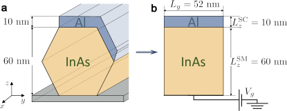
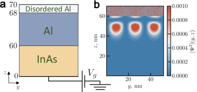
We consider the system shown in Fig. 1. The nanowires used in current experiments typically have a hexagonal shape as shown in Fig. 1 (a). The cross section of the wire, which we take to be the -plane, consists of a nm thick Al film (blue) covering 2 facets of InAs nanowire (orange). The electrostatic environment is controlled by a back-gate (gray). For practical reasons we do not explicitly treat this gate and the separating dielectric medium in our calculations, but rather take the gate into account only as a boundary condition for the potential in the wire. In order to convert this into the actual voltage applied to the gate (which is sample-dependent), the distance to the gate and the dielectric constant have to be taken into account. For the devices of interest, the length of the wire, , is much larger than its transverse dimensions .
The presence of the Al layer breaks the hexagonal symmetry of the nanowire cross section and, as shown in Fig. 2, causes the formation of an electrostatic potential that strongly confines the electrons close to the SM/Al interface. For this reason the hexagonal cross section of the wire can be well approximated by an effective rectangular cross section, as shown in Fig. 1 (b). We will henceforth refer to the effective wire with rectangular cross section as the slab model. By choosing for the slab model to be such that the number of cross sectional modes is the same as for the hexagonal cross section wire, the use of the slab model does not cause any significant loss of accuracy and significantly simplifies the numerical implementation and solution of the SP problem.
| Parameter | InAs | Al |
| Vurgaftman et al. (2001) | ||
| , eV | Schuwalow et al. | |
| Pidgeon et al. (1967) | ||
| , eV nm | van Weperen et al. (2015) | |
| , eV | Cochran and Mapother (1958) | |
| , meV | Cochran and Mapother (1958) | |
| , nm | ||
| , nm |
The Hamiltonian for the heterostructure in the normal state can be written as ()
| (1) | ||||
where the spatially-dependent effective mass , Fermi energy , spin-orbit coupling strength , and factor are equal to () for nm ( nm) and similarly for , , and ; are the momentum operators in the and direction, respectively; is the electrostatic potential, are the Pauli-matrices in spin space, and are the Bohr magneton and the external magnetic field, respectively. The values for the material parameters used henceforth are given in Table 1.
In this work we investigate bulk properties of the heterostructure. Therefore, we assume henceforth that the nanowire is infinitely long and translationally invariant along the direction. This allows one to use as a basis plane waves along the direction and to replace the operator in (1) by its eigenvalue. In the clean limit considered here, due to the finite-size quantization in the and directions, the spectrum of the system consists of effectively 1D subbands. We obtain the eigenvalues and eigenstates of the resulting Hamiltonian corresponding to these subbands via a mode decomposition in the direction and by replacing the derivatives with respect to with finite differences using a non-uniform grid Tan et al. (1990) with two different spacings corresponding to the semiconducting and superconducting components, respectively. The spacings are chosen such that in order to minimize discretization errors. Using a non-uniform spacing significantly alleviates the computational cost and allows us to systematically study the phase diagram of the problem.
In the absence of spin-orbit coupling and disorder the discrete modes along the direction are
| (2) |
with the different modes being decoupled. The spin-orbit coupling term hybridizes them Stanescu et al. (2011). The corresponding matrix elements are
| (3) | ||||
In the basis the Hamiltonian matrix takes the form
| (4) |
where is the matrix with elements given by Eq. (3), is the number of discrete modes along the direction considered and is the matrix obtained by projecting the Hamiltonian (1) for on this basis.
We treat the s-wave superconductor at the BCS mean-field level. The Bogoliubov-de-Gennes (BdG) Hamiltonian for the system can be written as
| (5) |
where are Pauli matrices in Nambu (particle-hole) space. We include the superconducting pairing only in the superconductor, i.e. for nm, where is the SC gap of Al (see Table 1), and for . In a finite magnetic field, the superconducting gap in the Al shell is suppressed due to the inclusion of a finite -factor for the Al (see Table 1). Given that the Al film is very thin, see Fig. 1, we neglect orbital effects due to the magnetic field.
II.1 Electrostatics
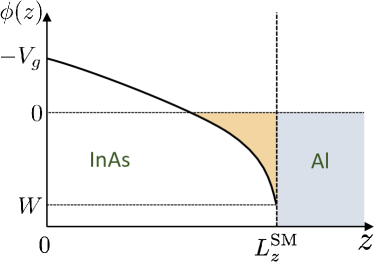
In order to obtain the electrostatic profile, one has to solve the SP equations self-consistently. Given that the BCS mean-field approximation breaks charge conservation this is a non-trivial task, see, e.g., discussion in Ref. Knapp et al. (2018). However, electrostatic screening of a metal is only weakly modified by the superconductivity with the small parameter being . As a consequence, to obtain the electrostatic potential within this accuracy the charge density entering the Poisson equation can be calculated neglecting the superconducting pairing, i.e. using the Hamiltonian instead of the full Hamiltonian . The effects of the spin-orbit coupling and Zeeman terms Vuik et al. (2016) on the total electron density profile are also very small and can be neglected. Thus, to solve the full problem we follow a two step approach: we first solve the SP problem in the normal state taking and to obtain the electrostatic profile. We then use the obtained electrostatic profile to find the eigenvalues and the eigenstates of the system for , , and different values of .
The first step consists in solving self-consistently the Schrödinger equation , requiring to vanish at the boundaries of the system, 111Note that the presence of -dependent masses, spin-orbit coupling and potentials does not allow to separate variables in and other directions and therefore a diagonalization of a Hamiltonian matrix would be required for every different set of momenta. and the Poisson equation
| (6) |
where , is the relative dielectric constant of the SM, see Tab. 1, and is the vacuum dielectric constant. The setup for the Poisson equation is shown in Fig. 2. At the boundary condition for is given by the band offset between the SM and the SC. The boundary condition at is set by the back gate. The coupled Schrödinger-Poisson equations are solved iteratively until convergence is achieved, using Anderson’s mixing algorithm Anderson (1965).
II.2 Band structure
The calculated electrostatic profile is inserted into the full Hamiltonian to obtain the band structure and the corresponding eigenstates of the nanowire. Since the chemical potential is included in the Hamiltonian, the effective Fermi energy for each band is set simply by the bottom of the band. We can find the Fermi momentum in each band, , by solving . The Fermi velocity is given by . In addition, from the eigenstates at we extract how strongly different subbands are coupled to the superconductor, which we define through the weight of the corresponding state in the superconductor
| (7) |
We define the gap as the minimum of the energy of the first excited state: . At zero magnetic field, gives an estimate for the induced gap .
III Results
In this section we discuss the results of our numerical simulations. We first discuss only the electrostatic problem for both a model of a hexagonal wire and the slab model introduced above. We then investigate the nature of the electronic states in a limit of strong coupling between the semiconductor and superconductor and discuss their superconducting properties at zero magnetic field. Then we study properties of the hybrid nanowires in a finite magnetic field and obtain estimates for the effective g-factor in the hybrid structure. We present the topological phase diagram and compare it with previous results Lutchyn et al. (2011); Stanescu et al. (2011). Finally, we present the results for the wires with the disorder potential present in the superconductor and show its impact on the induced gap and the phase diagram.
III.1 Electrostatics and density distribution
III.1.1 Hexagonal cross section
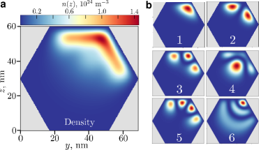
In order to obtain the correct number of subbands for a given gate configuration for the wire with the hexagonal cross section it is sufficient to solve the SP problem using the Thomas Fermi approximation and simply requiring the wave function to vanish at the boundaries of the cross section. The solution of the full SP problem is computationally expensive due to the shape of the cross section and unnecessary for the purpose of simply estimating the number of cross sectional modes. We perform this calculation in COMSOL and obtain eigenstates using the Kwant package Groth et al. (2014).
Our results are summarized in Fig. 3, where we show the density for all occupied modes below the Fermi energy. This calculation does not explicitly treat the aluminum shell; instead, it assumes that the only effect of the presence of the Al layer is to induce a band offset. We set this band offset to Schuwalow et al. , see Table 1. The approximations used to obtain the results of Fig 3 cause quantitative inaccuracies for the local density of states (LDOS) and the carrier density profile. However, these results are sufficiently accurate to estimate the number of electronic cross-sectional modes below the Fermi energy for a given . In addition, the results of Fig. 3 (a) show the qualitatively correct result that for most of the charge density is localized at the semiconductor (SM)-superconductor (SC) interface due to the strong band offset between the InAs and Al. This fact means that for the slab model, the thickness of the SM wire in the direction does not affect the electronic properties in a significant way as long as it is few times larger than the confinement length in the direction ( nm). The effective width of the slab model can then be fixed by requiring the number of subbands to be equal to the number of cross-sectional modes obtained from the hexagonal calculation, as long as is also larger than the confinement length in the direction. For the hexagonal cross section results show that there are six modes, see Fig. 3 (b). From this we obtain that for the slab model nm, larger than the confinement length for . In the remainder all the results are obtained using the effective slab model with nm width and nm thickness for the SM and nm for Al, as shown in Table 1.
III.1.2 Slab model
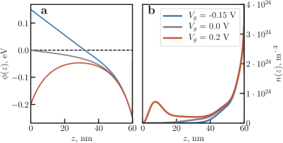
We now switch to the slab model, which explicitly treats the superconducting Al shell. We self-consistently solve the coupled Schrödinger-Poisson (SP) equations for three different values of to obtain the electrostatic potential and the density , respectively shown in panels (a) and (b) of Fig. 4. Since the Al shell is taken to be metallic with an extremely short screening length, the electrostatic potential is assumed to be constant throughout the Al. The dashed line in Fig. 4 (a) shows the Fermi level in Al. It is worth pointing out that because , including the pairing term for the Al makes only a negligible difference to the electrostatic profile.
For the electrostatic potential confines the carrier density in a layer about 20 nm wide close to the SM/Al interface, as shown in Fig. 4 (b). For the electrostatic potential is below the Fermi energy also on the gate side. This allows the accumulation of charges also near the gate, as shown by the result in Fig. 4 (b) for .
III.2 Nature of electronic states in strong-coupling limit
We now discuss the nature of the electronic states in the electrostatic environment determined by the gate as well as the band offset between the semiconducting wire and the metallic shell. In particular, we will investigate how strongly states are hybridized between the two materials depending on the gate voltage.
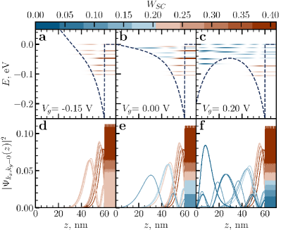
In the top panels of Fig. 5, we show the electrostatic profile (cf. Fig. 4) for three values of the gate voltage. The lower panels show the square of the wave function for all occupied subbands for the corresponding electrostatic profile. Here we have chosen the momentum of the band bottom, , so that all filled bands are included. The color scale in Fig. 5 indicates the weight of the wavefunctions in the superconductor (see Eqn. (7)). In the top panels, we have also superimposed horizontal lines showing the energy of the corresponding subbands; furthermore, the intensity of the lines shows the square magnitude of the wave functions, and in the semiconducting part the color scale indicates again the weight in the superconductor.
For the case of (middle column of panels), we find 9 hybridized subbands, some of which are mostly localized in the SM whereas the others have large weight in the superconductor 222Other 1D subbands in Al having effective Fermi energies larger than eV are not shown since they do not hybridize with the semiconductor subbands due to energy-momentum conservation. However, when Al is disordered, these subbands hybridize and, therefore, have to be taken into account. .
For the electrostatic potential confines the wave function in the SM to a very narrow region close to the SM/Al interface. Such confinement favors a strong hybridization of the SM and Al eigenstates, thus giving rise to states which have large weight in both the SM and Al. Such large hybridization is prevented in the absence of the confining electrostatic potential due to the large mismatch between the Fermi velocities of the two materials. The strong confining potential due to the band offset is therefore critical for the hybridization of the SM and Al states.
For , we see in Fig. 5 (c) that a number of subbands closer to the Fermi energy appear which are not confined to the interface, and instead have appreciable weight throughout the SM. These states have very small . Their contribution to the density can also be seen in panel (b) of Fig. 4 in the peak of the density near the gate.
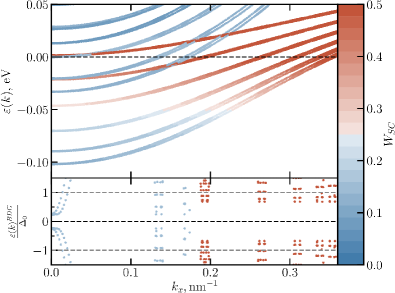
While one might naively expect that the lowest bands are most confined to the interface and thus hybridize most strongly, this is not reflected in the data shown in Fig. 5. To further elucidate which bands most strongly hybridize with the superconductor, we show the full band structure at in the top panel of Fig. 6. Here, color again indicates the weight of the state in the SC; however, in contrast to Fig. 5, we do not just consider . We observe that hybridization with the superconductor may depend strongly on , and in this case is generally strongest at large .
III.3 Superconducting properties at
We now turn our attention to the situation where the Al shell is in the superconducting state. The value of at correlates well with the magnitude of the induced superconducting gap for a given subband. From the discussion of the previous subsection, we can then immediately conclude that different subbands will have different values of . This is illustrated in the lower panel of Fig. 6, in which the subbands are shown for the case when , for energies of the order of . We see that bands with smaller (shown as more blue) also have smaller . The smallest value of is what fixes the superconducting gap for the SM-SC hybrid nanowire. This again emphasizes the importance of the strong confining potential to increase the hybridization between the two materials and thus a large induced gap.
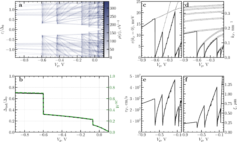
Figure 7 (a) shows the evolution of the DOS with . For V all subbands in the SM hybridize very strongly with the Al subbands and, thus, have a large induced SC gap. As a result, there are no subgap states below . As increases and the electrostatic potential becomes less confining, additional SM subbands become occupied for certain threshold values of . As shown in Figure 7 (a), the number of subbands jumps at . In some cases the additional subbands have a smaller value of resulting in a decrease of . From Fig. 7 (b) we can see that this happens for the threshold values of -0.6 and -0.06 V. For , as shown in Fig. 5 (d), some of the subbands have states that are not localized close to the SM-SC interface and for which is negligible. In this situation , and the system becomes gapless.
The evolution of with is shown in Fig. 7 (b), together with the evolution of . From this figure we see that for V, . Furthermore, these results indicate that the evolution of the nanowire’s superconducting gap with can be quite non-trivial and is closely related to . In order to have , strong confining potentials ( V) are necessary. Conversely, in the case of a positive gate voltage, there are occupied states in the SM (see right panels of Fig. 5) which are far away from the SC and, as a result, are weakly proximitized.
Figures 7 (c)-(f) show the evolution of , , , and with for the subband with the smallest induced superconducting gap, which determines for the system. For a fixed number of subbands, as increases , and grow, see Fig. 7 (c)-(e). Using the values of , and one can estimate the coherence length . From Fig. 7 (b) we see that change in preserving the number of occupied subbands leads to small changes in . Thus, the variations of are mostly due to the changes in , see Fig. 7 (f). We see that, as long as the number of subbands is constant, grows with and follows . The discontinuities in , , , and appear when the number of occupied subbands changes, see Fig. 7 (a)-(f).
III.4 Superconducting properties at finite magnetic fields
We now study how the properties of the SM-SC nanowire depend on the presence of the external magnetic field aligned along the longitudinal direction of the wire. As discussed in Sec. II, in our treatment the magnetic field enters only via the Zeeman term. For , orbital effect of the applied magnetic field is small since the SC is only 10 nm thick and in the regime of interest the wave functions in the SM are confined to the SM-SC interface within 20 nm range.
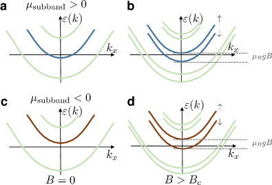
We start by investigating Zeeman splitting for the nanowire with multi-subband occupancy. The corresponding band structure is shown in Fig. 8 (a). Let’s consider the gate voltage such that the highest occupied subband (shown in blue color) has small Fermi energy. The application of a magnetic field splits the subband and, at some critical field , drives the minority subband across the Fermi level (provided is less than the critical field of the superconductor). This is illustrated in Fig. 8 (b). At this point, the majority subband becomes the highest occupied band, and, thus, many properties such as the Fermi energy, Fermi velocity and Fermi momentum change discontinuously.
Another scenario corresponds to Fig. 8 (c), where a band is just above the chemical potential. In this case, the gap of the system is determined by the lower occupied subband (shown in green). An increasing magnetic field splits the lowest unoccupied band (shown in red) and eventually it becomes occupied.
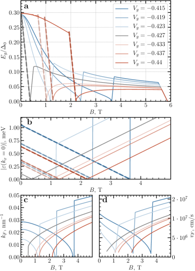
In both these cases, we end up with an odd number of occupied subbands at large enough magnetic fields and, thus, the nanowire can be driven into the topological regime. However, the evolution of the gap with the magnetic field is drastically different in these two cases. This can seen in Fig. 9 which shows the evolution with magnetic field of the spectral gap , effective Fermi energy for the highest occupied subband, and corresponding , , and for different gate voltages close to the the threshold value V. This threshold value, corresponding to the gray curves in Fig. 9, corresponds to the gate voltage at which the relevant subband has exactly zero effective Fermi energy. As increases from zero the gap decreases and eventually vanishes at corresponding to the topological phase transition. For , the nanowire is driven into the spinless regime with p-wave pairing potential. The p-wave gap exhibits a non-monotonic dependence on the magnetic field, and eventually vanishes because s-wave superconductor becomes normal. For our parameters this occurs at T. Note that we do not take into account orbital effects here so in practice may vanish before that.
The blue family of curves in Fig. 9 (a) correspond to the case when a highest-occupied subband has a small Fermi energy at zero field (top panels of Fig. 8). In that case, the gap at zero field is already set by the band that will eventually be split to give rise to topological superconductivity, and, thus, the gap evolves as a smooth function for . At the minority subband crosses the Fermi level, and the topological gap is opened in the majority subband. As dicussed above, the properties of the Fermi points evolve discontinuously across the transition (panels b,c,d), and the gap increases rapidly into the topological phase (panel a).
At more negative gate voltages, the situation shown in Fig. 8 (c) and (d) is realized, corresponding to the red lines in Fig. 9. Here, the gap at is determined by the next occupied subband. Upon the application of a magnetic field, the distance between the majority subband and the chemical potential eventually becomes smaller than the gap induced in the next-highest subband. This distance thus sets the spectral gap. The discontinuity of the gap function can be seen in Fig. 9 (a). At the topological gap is opened in the majority subband. In this cases, we plot in Fig. 9 the properties of the Fermi points only for the subbands that eventually become topological, and thus plot no values below the topological phase transition.
It is very interesting to notice that the size of the induced superconducting gap for does not necessarily correlate with the size of the topological gap. This can be understood from the fact that the topological gap for is always opened in the same band, whereas the at is opened in a different band when becomes smaller than V. As can be seen from Fig. 9 (c) the Fermi momentum for , which corresponds always to the same band, increases with . The topological gap increases with since the effective Rashba field is stronger at higher momentum, allowing the -wave pairing to induce a larger gap. This is a very important result because at sets a crucial scale for the robustness of a topological qubit against error sources such as thermal fluctuations, diabatic corrections, disorder Cheng et al. (2012); Liu et al. (2017); Knapp et al. (2018); Fu et al. (2018) etc.
III.5 Effective g-factor
A crucial quantity to characterize the semiconductor-superconductor system is the effective g-factor of the hybrid system. Due to the drastically different g-factors in the two materials, this will depend intricately on the wave function hybridization between them. Furthermore, the g-factor is crucial in enabling a large and robust topological phase, since a large g-factor is necessary for the topological phase transition to occur at a magnetic field well below the critical value at which the Al shell is driven normal. A large effective is thus very helpful in achieving a sufficient separation between these scales.
The effective g-factor can be obtained from studying the Zeeman splitting of bands at , as illustrated in Fig. 8. In particular, since at the spin-orbit terms in the Hamiltonian (4) vanish, the spin-splitting of the bands at is entirely determined by the Zeeman term. As the change of the energy levels is linear with the magnetic field, the absolute value of the g-factor can be extracted as . This linear fit for is illustrated in Fig. 9b with dashed lines. Note that when the gate voltage is such that the closest subband to the Fermi level is unoccupied (case (c) in Fig. 8), the slope near the gap-closing is the same as the one at , allowing for a reliable extraction of the g-factor from the tunneling conductance measurements Vaitiekénas et al. (2017). This is shown in Fig. 9a by the dashed lines.
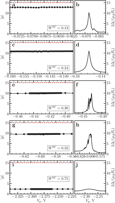
In Fig. 10 we study the dependence of the extracted g-factor on the applied gate voltage in the vicinity of the threshold values at which the number of subbands change (see Fig. 7). As expected, we find every subband to be characterized by an almost constant g-factor, with significant changes occuring only at transitions between bands. When the hybridization between semi- and superconductor is weak, the g-factor is close to the bare semiconductor value . Conversely, when the voltage is very negative (the value from Fig. 7 is written in every panel) and the hybridization between semi- and superconductor is strong the g-factor is almost as small as the bare superconducting g-factor .
Additional information can be extracted from the ratio of the induced gap to the critical field, shown in the right column of Fig. 10. This quantity is easily accessible in experiments, and has been used in the experimental literature as a proxy for the g-factor Vaitiekénas et al. (2017). Our results clearly show that unlike the g-factor, this quantity has a strong dependence on gate voltage over relatively small gate voltage variations. In particular, a resonant structure appears with a peak that corresponds to the gate voltage being tuned to the threshold value at which the subband crosses the effective chemical potential. Only at this point does this quantity reaches the values of the effective g-factor shown in the left column.
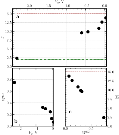
Figure 11 (a) shows the value of for different topological regions (see also the discussion in Sec. III.6). We see that as becomes more negative the g-factor becomes smaller and approaches the value of in the SC. As stated above this is due to the fact that as becomes more negative the hybridization between SM and SC states becomes stronger as clearly shown by the evolution of , see Fig. 11 (b). Larger negative values of create an electrostatic potential that more strongly confines the SM states at the SM-SC interface. The tighter confinement results in a stronger hybridization between SM and SC states. Figure 11 (c) summarizes the important relation between strength of the hybridization between SM and SC states and the g-factor by showing the dependence of on . We see that qualitatively scales linearly with .
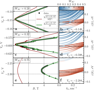
III.6 Topological phase diagram
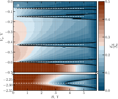
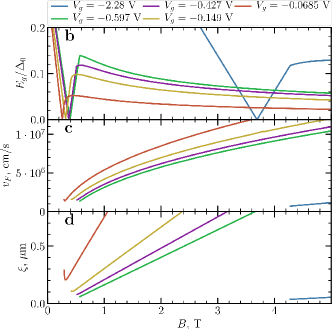
Figure 12 (a) shows the topological phase diagram in the plane. This is one of the most important results of this work: it relates the nature of the superconducting state of the quasi-1D hybrid nanowire to the experimentally relevant and tunable quantities – the gate voltage and the external magnetic field – rather than more abstract quantities such as the Fermi energy of the subbands and the Zeeman splitting, which are dependent on applied electric field. As discussed above, the relation between and the parameters characterizing the nanowire band structure, such as the subbands’ Fermi energy and induced superconducting gap, is highly non-trivial given the nonlinear nature of the SP problem and the presence of multiple subbands. For this reason, simplified models in which the subband chemical potential is assumed to be directly proportional to in general cannot be used to obtain a reliable phase diagram in the plane. Similarly, we have shown that for the g-factor we cannot take the bare value of the SM. One qualitative feature that emerges from the results shown in Fig. 12 (a) is how the shape and size of the topological regions depend on . We see that for very large negative the critical magnetic field is higher than that for small negative values of . This is due to the fact that the hybridization of the SM’s and SC’s states is stronger for larger negative and therefore the effective magnitude of is much smaller than causing an increase of the critical field.
The topological phase diagram can be obtained by calculating the topological index (Majorana number) Kitaev (2001); Lutchyn et al. (2011); Stanescu et al. (2011):
| (8) |
where is an antisymmetric matrix which defines the Hamiltonian of the system in the Majorana basis. The negative/positive sign of corresponds to a topologically trivial/non-trivial phase. The latter supports Majorana zero modes at the ends of the nanowire. In the continuum limit, the lattice spacing , and the sign of is fixed. Thus, the topological quantum phase transition corresponds to a change of . Note that the topological phase transition in this case is accompanied by a vanishing quasiparticle gap at which provides another way of determining of the phase boundary.
It is illuminating to compare the phase diagram of Fig.12 (a) with previous studies Lutchyn et al. (2011); Stanescu et al. (2011). Adapting the results of Refs. Lutchyn et al., 2010; Oreg et al., 2010; Lutchyn et al., 2011, the critical magnetic field for the topological transition is given by
| (9) |
where defines the position of the band bottom at relative to the Fermi energy in the superconductor and is the effective g-factor. As follows from the discussion above, the effective g-factor can be obtained by calculating Zeeman splitting at .
Having obtained the dependence of , and on , one can draw the boundaries in the plane of the topological phase diagram using Eq. (9). These boundaries are shown in green in the left panels of Fig. 13. We see that they exactly match the boundaries obtained by identifying the value of , , where the gap is closing . In particular, Eq. (9) gives the correct boundaries if the renormalization of the g-factor is taken into account. On the other hand, if in Eq. (9) we use the bare SM g-factor, Eq. (9) gives incorrect boundaries, shown in red in the left panels of Fig. 13. The boundaries obtained using the bare SM g-factor overestimate the size of the topological region, especially when is strongly negative, as shown in the bottom left panel of Fig. 13. As discussed above, this is due to the fact that the value of the g-factor, in the strong coupling regime, is strongly renormalized by the hybridization between the SM and SC states. The right panels in Fig. 13 show the band structure of the SM-SC nanowire close to the Fermi energy when for the appropriate values of . We see that for very negative values of , bottom panel, the SM states are very strongly hybridized with the SC states. This result is consistent with the fact that for this case is much smaller than and therefore the topological region is much smaller that we would have obtained assuming .
Figures 12 (b)-(d) show the dependence of the gap (b), Fermi velocity (c), and coherence length (d) on the magnetic field, for , for different domes in the topological phase diagram shown in Fig. 12 (a). To obtain these figures we use the representative gate voltages indicated by the white dashed lines in Fig. 12 (a). For fixed magnetic field, the gap decreases with the gate voltage while the Fermi velocity increases. As a consequence, the coherence length increases. The results of Fig. 12 (d) show that when the topological gap is maximal, has values in the nm range, and that grows linearly with for . The growth of with is slower for more negative gate voltages, a reflection of the fact that for larger negative gate voltages the effective g-factor is smaller due to the stronger hybridization of the SM’s and SC’s states. The results of Fig. 12 (d) are important for the design of Majorana-based qubits since their topological protection relies on the exponentially-small splitting of Majorana zero modes which, in turn, strongly depends on the coherence length.
III.7 Effect of disorder in SC-SM heterostructures
Disorder is ubiquitous in solid-state systems and has a strong impact on the physical properties of proximitized nanowires. It has been shown that disorder in the SM and at the SM-SC interface is detrimental to the topological phase Potter and Lee (2011a, b); Lobos et al. (2012); Lutchyn et al. (2012); Sau et al. (2012); Tkachov (2013); Sau and Das Sarma (2013); Hui et al. (2015); Cole et al. (2016); Liu et al. (2018). However, in the MBE-grown SC-SM heterostructures Krogstrup et al. (2015); Lutchyn et al. (2018) disorder effects are minimized resulting in high quality SMs as well as SM-SC interfaces. The SC (i.e. Al) is also nominally of high quality but its outer surface is covered by an amorphous oxide layer, see Fig. 14. Therefore, the scattering from the outer boundary randomizes the motion of quasiparticles in the SC. Due to the large effective mass mismatch and the conservation of the momentum at SM-SC interface, disorder in the SC is not expected to interfere with the observation and manipulation of MZMs Lutchyn et al. (2012); Liu et al. (2018); Sticlet et al. (2017). Nevertheless, as we will show it can strongly affect key quantities of the proximitized nanowire, such as and the critical field , as well as their dependence on the external gate voltage.
We model disorder by adding the random potential to the Hamiltonian (1). Due to the computational complexity of the problem we consider here the disorder potential (i.e. homogeneous along the wire). Such potential hybridizes different and subbands which effectively increases density of states in the SC. In contrast to Eq. (4) the modes in the direction are not separable anymore, and we have to resort to a numerical solution of the full Hamiltonian, leading to a much greater numerical complexity. We calculate results for a given disorder realization and then average physical observables over approximately 25 disorder realizations.
We model the amorphous oxide layer in the superconductor by adding a disorder potential within nm from the outer surface of the SC, see Fig. 14. We assume the disorder potential to have zero average and to be spatially uncorrelated:
| (10) |
Here denotes averaging over disorder realizations, parametrizes the disorder strength, and corresponds to the density of impurities. Considering the finite spatial resolution in the numerical calculation and the uniform box distribution of the disorder with the amplitude , is related to as , where is the volume of a single cell of the spatial discretization (see Table 1), that we set to be uniform in the region where the disorder is located. We vary in the parameter range eV which corresponds to the effective mean-free length larger than 10nm.
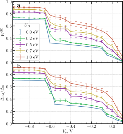
One of the main effects of the disorder in the SC is to break the conservation of the momentum and to induce broadening of the SC subbands which effectively increases the number of superconducting subbands hybridizing with a given SM mode. This effect is shown in Fig. 14b where we plot the wavefunction probability density: the wavefunction probability in the SC is random, which corresponds to chaotic motion of quasiparticles, whereas the one in the SM preserves periodicity in -direction. One may notice that disorder leads to an enhancement of , as shown in Fig. 15 (a). As increases more SM’s subbands couple to the SC’s subbands with comparable strength and therefore changes of that “push” different SM’s subbands to the Fermi level do not cause sudden jumps of in contrast to the clean case. The behavior of versus correlates with the dependence of on , as shown in Fig. 15 (b). Similar to the clean case (see Fig. 7) there is a one-to-one correspondence between the weight in SC and the induced gap. As follows from Fig. 15 the disorder in the SC increases the range of values of for which SC-SM heterostructure is in the strong tunneling regime which agrees qualitatively with the recent experiments Vaitiekénas et al. (2017); de Moor et al. (2018).
As discussed in the previous sections a large implies not only a large but also a reduced g-factor. Since the presence of disorder increases (all other parameters being equal), the reduction of the g-factor is also enhanced. From Eq. (9), we see that both the increase of and the reduction of will cause an increase of the minimal critical magnetic field for the topological phase transition. Considering that the disorder in the SC does not affect directly the SM’s subbands, in particular their energy at , we conclude that the dominant effect of the disorder in the SC on the topological phase diagram is to cause an increase of . Therefore, in the presence of disorder the topological regions of Fig. 12 (a) move towards larger values of . The shift in of the boundaries of the topological phase appears to be negligible.
To study this more quantitatively, we determine the minimal critical field for a topological “dome” as previously shown in Fig. 12; we denote this minimal field as . Figure 16 shows for different values of . The open symbols in Fig. 16 represent the values of for different disorder realizations whereas the solid symbols correspond to the values of averaged over 25 disorder realizations. These results clearly demonstrate that as increases increases as well, mostly due to a decrease of , and results in a reduction of the area of the topological regions in the plane. For very large disorder strengths and negative gate voltages, the effective g-factor becomes so small so that becomes larger than the critical field of Al.
We conclude this section by summarizing that the main effect of disorder in SC is to increase the coupling between SM and SC, resulting in larger induced gap and critical fields to cross the topological phase transition.
IV Summary and conclusions
We have studied properties of SM-SC nanowires in the presence of strong external electric fields. Our method is based on self-consistent Schrödinger-Poisson calculations which treat the semiconductor and the superconductor on equal footing. This approach allows one to take into account several semiconductor subbands which, we believe, are present in current experimental devices. We find that the treatment of the SM and SC at the same level is necessary to describe the strong-coupling regime characteristic to the high-quality epitaxial nanowires Krogstrup et al. (2015). Such hybrid nanowires are very promising for the topological quantum computing applications as they exhibit large proximity-induced gaps and very low subgap conductance Chang et al. (2015); Deng et al. (2016); Zhang et al. (2018).
One of the most important results of our work is to provide an insight regarding the necessary conditions for achieving the strong-coupling regime in proximitized nanowires. We find that one of the key ingredients is the presence of an accumulation layer at the interface between the SM and the SC. The presence of an accumulation layer implies a strong confinement of the semiconductor wave function close to the SM-SC interface. Without such confinement, the significant mismatch between the Fermi velocities of SM and SC would significantly reduce the induced gap. This conclusion has recently been supported by angle-resolved photoemission spectroscopy experiments that have shown that in epitaxial InAs/Al systems the band offset is negative and therefore an electron accumulation layer is present.
We have investigated the effect of an external electric field which can be used to modify the confining potential and, thus, modify properties of electronic states in SM-SC devices. We find that external electric field can be used to change the number of subbands in the semiconductor, tunneling rate, induced gap, magnitude of the effective factor, coherence length etc. Our results show that the relation between and the quantities characterizing the electronic state of SM-SC quasi-1D nanowires is not trivial. The understanding of the interplay of , number of subbands, and electronic properties is one of the most important results of our work.
We have obtained the topological phase diagram as a function of the gate voltage and magnetic field . Previous works calculated the topological phase diagram in terms of phenomenological parameters such as effective chemical potential. Our work is the first to present a phase diagram in terms of , the experimentally relevant and tunable quantity, instead of the chemical potential. We find that in the strong coupling regime the renormalization of the factor due to the strong hybridization between the SM’s and the SC’s states can significantly modify the topological phase diagram. For typical setups, the of the SC is smaller (in absolute value) than the SM’s factor, and so the strong hybridization reduces the factor causing a decrease in the plane of the region where the system is in the topological phase.
Finally, we took into account effect of disorder. There is a large body of papers investigating effect of the disorder in the semiconductor Motrunich et al. (2001); Brouwer et al. (2011); Stanescu et al. (2011); Akhmerov et al. (2011); Liu et al. (2012); Lobos et al. (2012); Adagideli et al. (2014); Hegde and Vishveshwara (2016) and at the interface Takei et al. (2013) concluding that disorder leads to the subgap density of states (i.e. states below the induced gap). However, given the observation of a very small subgap density of states in recent experiments on high-quality proximitized nanowires Chang et al. (2015); Deng et al. (2016); Zhang et al. (2018); Nichele et al. (2017), we believe that the semiconductor, as well as SC-SM interface, are quite clean. The situation with Al is less clear since the presence of the native oxide covering Al may lead to significant impurity scattering. The effect of the disorder in the superconductor that it relaxes the constraint on momentum conservation and leads to the enhancement of the induced SC gap and critical field. Once again the optimization of the tunneling rate between SM-SC is very important Lutchyn et al. (2012); Liu et al. (2018).
Our work has important implications for current and future experiments aiming to realize Majorana-based topological qubits using SM-SC heterostructures as it allows one to optimize Majorana devices by tuning key parameters, , , and with gates. Our results show that in the strong coupling the renormalization of can be quite significant increasing the minimal magnetic field necessary to drive the system into the topological phase. Thus, there is a sweet spot, and it is beneficial to operate in the intermediate coupling regime. This is critical information to design experiments aimed at realizing MZMs.
Finally, we discuss some limitations of our model. First, the disorder is two-dimensional, leading to a qualitatively similar picture as in the disorder-free case. Impurities in the SC may induce subgap states Lutchyn et al. (2012); Hui et al. (2015); Cole et al. (2016); Liu et al. (2018) that can be captured in a fully three-dimensional simulation. Another limitation of our model is the lack of orbital effects due to the magnetic field. Due to the strong geometry dependence of the orbital effect Winkler et al. (2017); Wójcik and Nowak (2018), however, a careful treatment of it needs to go beyond the slab model discussed here de Moor et al. (2018); Winkler et al. .
Finally, we emphasize that, although in this work we focused on InAs/Al hybrid nanowires, the Schrödinger-Poisson approach proposed in this work can be used to study other heterostructures such as InSb/Al nanowires, two-dimensional SM-SC heterostructure and the quasi 1D channels created by electrostatic confinement in such structures.
Note added. After our arXiv posting, three other preprints on a similar topic appeared Woods et al. (2018); Mikkelsen et al. (2018); Reeg et al. (2018). These manuscripts, as ours, present numerical approaches aimed at a more quantitative description of semiconductor-superconductor heterostructures. Reference Woods et al., 2018 studies the electrostatic environment of nanowires in the weak coupling regime. Ref. Mikkelsen et al., 2018 discusses the electrostatic environment in the presence of metallic Al and focuses on the normal-state band structure of the quasi-one-dimensional heterostructure. Reference Reeg et al., 2018 studies the renormalization of the semiconductor band structure by the proximity to the bulk superconductor in the strong coupling regime neglecting electrostatic effects.
V Acknowledgments
We are grateful to Mingtang Deng, Karsten Flensberg, John Gamble, Jan Gukelberger, Peter Krogstrup, Bas Nijholt, Saulius Vaitiekénas, Adriaan Vuik, Michael Wimmer, and Hao Zhang for stimulating discussions. ER acknowledges support from NSF-DMR-1455233, ONR-N00014-16-1-3158, and ARO-W911NF-16-1-0387.
References
- Beenakker (2013) C.W.J. Beenakker, “Search for Majorana Fermions in Superconductors,” Annu Rev Condens Matter Phys 4, 113–136 (2013).
- Alicea (2012) Jason Alicea, “New directions in the pursuit of Majorana fermions in solid state systems,” Rep. Prog Phys 75, 076501 (2012).
- Leijnse and Flensberg (2012) Martin Leijnse and Karsten Flensberg, “Introduction to topological superconductivity and Majorana fermions,” Semicond Sci Technol 27, 124003 (2012).
- Stanescu and Tewari (2013) T D Stanescu and S Tewari, “Majorana fermions in semiconductor nanowires: Fundamentals, modeling, and experiment,” J Phys Condens Matter 25, 233201 (2013).
- Elliott and Franz (2015) Steven R Elliott and Marcel Franz, “Colloquium : Majorana fermions in nuclear, particle, and solid-state physics,” Rev Mod Phys 87, 137–163 (2015).
- Das Sarma et al. (2015) Sankar Das Sarma, Michael Freedman, and Chetan Nayak, “Majorana zero modes and topological quantum computation,” Npj Quantum Inf 1, 15001 (2015).
- Sato and Fujimoto (2016) Masatoshi Sato and Satoshi Fujimoto, “Majorana Fermions and Topology in Superconductors,” J Phys Soc Jpn. 85, 072001 (2016).
- Aguado (2017) R Aguado, “Majorana quasiparticles in condensed matter,” (2017), arXiv:cond-mat.supr-con/1711.00011 .
- Lutchyn et al. (2018) R M Lutchyn, E P A M Bakkers, L P Kouwenhoven, P Krogstrup, C M Marcus, and Y Oreg, “Majorana zero modes in superconductor–semiconductor heterostructures,” Nat Rev Mater 3, 52–68 (2018).
- Read and Green (2000) N Read and Dmitry Green, “Paired states of fermions in two dimensions with breaking of parity and time-reversal symmetries and the fractional quantum Hall effect,” Phys Rev B 61, 10267–10297 (2000).
- Ivanov (2001) D A Ivanov, “Non-Abelian Statistics of Half-Quantum Vortices in p-wave superconductors,” Phys Rev Lett 86, 268–271 (2001).
- Kitaev (2001) A Yu Kitaev, “Unpaired Majorana fermions in quantum wires,” Phys.-Uspekhi 44, 131–136 (2001).
- Moore and Read (1991) Gregory Moore and Nicholas Read, “Nonabelions in the fractional quantum hall effect,” Nucl Phys B 360, 362–396 (1991).
- Bonderson et al. (2008) Parsa Bonderson, Michael Freedman, and Chetan Nayak, “Measurement-Only Topological Quantum Computation,” Phys Rev Lett 101, 010501 (2008).
- Wilczek (2009) Frank Wilczek, “Majorana returns,” Nat Phys 5, 614–618 (2009).
- Stern (2010) Ady Stern, “Non-Abelian states of matter,” Nature 464, 187–193 (2010).
- Brouwer (2012) P. W. Brouwer, “Enter the Majorana Fermion,” Science 336, 989–990 (2012).
- Lee (2014) Patrick A Lee, “Seeking out Majorana under the microscope,” Science 346, 545–546 (2014).
- Kitaev (2003) A.Yu. Kitaev, “Fault-tolerant quantum computation by anyons,” Ann Phys N 303, 2–30 (2003).
- Nayak et al. (2008) C Nayak, S.H̃. Simon, A Stern, M Freedman, and S Das Sarma, “Non-Abelian anyons and topological quantum computation,” Rev Mod Phys 80, 1083–1159 (2008).
- Fu and Kane (2008) Liang Fu and C. L. Kane, “Superconducting Proximity Effect and Majorana Fermions at the Surface of a Topological Insulator,” Phys Rev Lett 100, 096407 (2008).
- Fu and Kane (2009) Liang Fu and C L Kane, “Josephson current and noise at a superconductor/quantum-spin-Hall-insulator/superconductor junction,” Phys Rev B 79, 161408 (2009).
- Cook and Franz (2011) A Cook and M Franz, “Majorana fermions in a topological-insulator nanowire proximity-coupled to an s-wave superconductor,” Phys Rev B 84, 201105 (2011).
- Sun et al. (2016) Hao-Hua Sun, Kai-Wen Zhang, Lun-Hui Hu, Chuang Li, Guan-Yong Wang, Hai-Yang Ma, Zhu-An Xu, Chun-Lei Gao, Dan-Dan Guan, Yao-Yi Li, Canhua Liu, Dong Qian, Yi Zhou, Liang Fu, Shao-Chun Li, Fu-Chun Zhang, and Jin-Feng Jia, “Majorana Zero Mode Detected with Spin Selective Andreev Reflection in the Vortex of a Topological Superconductor,” Phys Rev Lett 116, 257003 (2016).
- Sau et al. (2010) Jay D. Sau, Sumanta Tewari, Roman M. Lutchyn, Tudor D. Stanescu, and S. Das Sarma, “Non-Abelian quantum order in spin-orbit-coupled semiconductors: Search for topological Majorana particles in solid-state systems,” Phys Rev B 82, 214509 (2010).
- Alicea (2010) Jason Alicea, “Majorana fermions in a tunable semiconductor device,” Phys Rev B 81, 125318 (2010).
- Lutchyn et al. (2010) Roman M. Lutchyn, Jay D. Sau, and S Das Sarma, “Majorana Fermions and a Topological Phase Transition in Semiconductor-Superconductor Heterostructures,” Phys Rev Lett 105, 077001 (2010).
- Oreg et al. (2010) Yuval Oreg, Gil Refael, and Felix von Oppen, “Helical Liquids and Majorana Bound States in Quantum Wires,” Phys Rev Lett 105, 177002 (2010).
- Chung et al. (2011) Suk Bum Chung, Hai-Jun Zhang, Xiao-Liang Qi, and Shou-Cheng Zhang, “Topological superconducting phase and Majorana fermions in half-metal/superconductor heterostructures,” Phys Rev B 84, 060510 (2011).
- Duckheim and Brouwer (2011) Mathias Duckheim and Piet W Brouwer, “Andreev reflection from noncentrosymmetric superconductors and Majorana bound-state generation in half-metallic ferromagnets,” Phys Rev B 83, 054513 (2011).
- Liu et al. (2012) Jie Liu, Andrew C Potter, K T Law, and Patrick A Lee, “Zero-Bias Peaks in the Tunneling Conductance of Spin-Orbit-Coupled Superconducting Wires with and without Majorana End-States,” Phys Rev Lett 109, 267002 (2012).
- Choy et al. (2011) T.-P. Choy, J M Edge, A R Akhmerov, and C W J Beenakker, “Majorana fermions emerging from magnetic nanoparticles on a superconductor without spin-orbit coupling,” Phys Rev B 84, 195442 (2011).
- Martin and Morpurgo (2012) Ivar Martin and Alberto F Morpurgo, “Majorana fermions in superconducting helical magnets,” Phys Rev B 85, 144505 (2012).
- Nadj-Perge et al. (2013) S Nadj-Perge, I. K. Drozdov, B. A. Bernevig, and Ali Yazdani, “Proposal for realizing Majorana fermions in chains of magnetic atoms on a superconductor,” Phys Rev B 88, 020407 (2013).
- Klinovaja et al. (2013) Jelena Klinovaja, Peter Stano, Ali Yazdani, and Daniel Loss, “Topological Superconductivity and Majorana Fermions in RKKY Systems,” Phys Rev Lett 111, 186805 (2013).
- Braunecker and Simon (2013) Bernd Braunecker and Pascal Simon, “Interplay between Classical Magnetic Moments and Superconductivity in Quantum One-Dimensional Conductors: Toward a Self-Sustained Topological Majorana Phase,” Phys Rev Lett 111, 147202 (2013).
- Vazifeh and Franz (2013) M. M. Vazifeh and M Franz, “Self-Organized Topological State with Majorana Fermions,” Phys Rev Lett 111, 206802 (2013).
- Pientka et al. (2013) Falko Pientka, Leonid I. Glazman, and Felix von Oppen, “Topological superconducting phase in helical Shiba chains,” Phys Rev B 88, 155420 (2013).
- Nakosai et al. (2013) Sho Nakosai, Yukio Tanaka, and Naoto Nagaosa, “Two-dimensional p-wave superconducting states with magnetic moments on a conventional s-wave superconductor,” Phys Rev B 88, 180503 (2013).
- Kim et al. (2014) Younghyun Kim, Meng Cheng, Bela Bauer, Roman M Lutchyn, and S Das Sarma, “Helical order in one-dimensional magnetic atom chains and possible emergence of Majorana bound states,” Phys Rev B 90, 060401 (2014).
- Brydon et al. (2015) P. M. R. Brydon, S Das Sarma, Hoi-Yin Hui, and Jay D. Sau, “Topological Yu-Shiba-Rusinov chain from spin-orbit coupling,” Phys Rev B 91, 064505 (2015).
- Li et al. (2014) Jian Li, Hua Chen, Ilya K Drozdov, A Yazdani, B Andrei Bernevig, and A H MacDonald, “Topological superconductivity induced by ferromagnetic metal chains,” Phys Rev B 90, 235433 (2014).
- Heimes et al. (2014) Andreas Heimes, Panagiotis Kotetes, and Gerd Schön, “Majorana fermions from Shiba states in an antiferromagnetic chain on top of a superconductor,” Phys Rev B 90, 060507 (2014).
- Röntynen and Ojanen (2015) Joel Röntynen and Teemu Ojanen, “Topological Superconductivity and High Chern Numbers in 2D Ferromagnetic Shiba Lattices,” Phys Rev Lett 114, 236803 (2015).
- Nadj-Perge et al. (2014) S Nadj-Perge, I. K. Drozdov, J Li, H Chen, S Jeon, J Seo, A. H. MacDonald, B. A. Bernevig, and A Yazdani, “Observation of Majorana fermions in ferromagnetic atomic chains on a superconductor,” Science 346, 602–607 (2014).
- Ruby et al. (2015) Michael Ruby, Falko Pientka, Yang Peng, Felix von Oppen, Benjamin W Heinrich, and Katharina J Franke, “End States and Subgap Structure in Proximity-Coupled Chains of Magnetic Adatoms,” Phys Rev Lett 115, 197204 (2015).
- Pawlak et al. (2016) Rémy Pawlak, Marcin Kisiel, Jelena Klinovaja, Tobias Meier, Shigeki Kawai, Thilo Glatzel, Daniel Loss, and Ernst Meyer, “Probing atomic structure and Majorana wavefunctions in mono-atomic Fe chains on superconducting Pb surface,” Npj Quantum Inf 2, 16035 (2016).
- Zhang et al. (2016) Junhua Zhang, Younghyun Kim, E Rossi, and Roman M Lutchyn, “Topological superconductivity in a multichannel Yu-Shiba-Rusinov chain,” Phys Rev B 93, 024507 (2016).
- Mourik et al. (2012) V Mourik, K Zuo, S M Frolov, S R Plissard, E P A M Bakkers, and L P Kouwenhoven, “Signatures of Majorana Fermions in Hybrid Superconductor-Semiconductor Nanowire Devices,” Science 336, 1003–1007 (2012).
- Rokhinson et al. (2012) Leonid P Rokhinson, Xinyu Liu, and Jacek K Furdyna, “The fractional a.c. Josephson effect in a semiconductor–superconductor nanowire as a signature of Majorana particles,” Nat Phys 8, 795–799 (2012).
- Deng et al. (2012) M T Deng, C L Yu, G Y Huang, M Larsson, P Caroff, and H Q Xu, “Anomalous Zero-Bias Conductance Peak in a Nb–InSb Nanowire–Nb Hybrid Device,” Nano Lett 12, 6414–6419 (2012).
- Churchill et al. (2013) H. O. H. Churchill, V Fatemi, K Grove-Rasmussen, M. T. Deng, P Caroff, H. Q. Xu, and C. M. Marcus, “Superconductor-nanowire devices from tunneling to the multichannel regime: Zero-bias oscillations and magnetoconductance crossover,” Phys Rev B 87, 241401 (2013).
- Das et al. (2012) Anindya Das, Yuval Ronen, Yonatan Most, Yuval Oreg, Moty Heiblum, and Hadas Shtrikman, “Zero-bias peaks and splitting in an Al–InAs nanowire topological superconductor as a signature of Majorana fermions,” Nat Phys 8, 887–895 (2012).
- Finck et al. (2013) A D K Finck, D J Van Harlingen, P K Mohseni, K Jung, and X Li, “Anomalous Modulation of a Zero-Bias Peak in a Hybrid Nanowire-Superconductor Device,” Phys Rev Lett 110, 126406 (2013).
- Chang et al. (2015) W Chang, S.M̃. Albrecht, T.S̃. Jespersen, F Kuemmeth, P Krogstrup, J Nygård, and C.M̃. Marcus, “Hard Gap in Epitaxial Superconductor-Semiconductor Nanowires,” Nat Nanotechnol 10, 232 (2015).
- Krogstrup et al. (2015) P. Krogstrup, N. L. B. Ziino, W. Chang, S. M. Albrecht, M. H. Madsen, E. Johnson, J. Nygård, C. M. Marcus, and T. S. Jespersen, “Epitaxy of semiconductor–superconductor nanowires,” Nat Mater 14, 400–406 (2015).
- Albrecht et al. (2016) S. M. Albrecht, A. P. Higginbotham, M Madsen, F Kuemmeth, T. S. Jespersen, J Nygård, P Krogstrup, and C. M. Marcus, “Exponential protection of zero modes in Majorana islands,” Nature 531, 206–209 (2016).
- Gül et al. (2016) Önder Gül, Hao Zhang, Jouri D. S. Bommer, Michiel W. A. de Moor, Diana Car, Sébastien R. Plissard, Erik P. A. M. Bakkers, Attila Geresdi, Kenji Watanabe, Takashi Taniguchi, and Leo P. Kouwenhoven, “Ballistic Majorana nanowire devices,” Nat Nanotechnol 13, 192–197 (2016).
- Chen et al. (2017) Jun Chen, Peng Yu, John Stenger, Moïra Hocevar, Diana Car, Sébastien R. Plissard, Erik P. A. M. Bakkers, Tudor D. Stanescu, and Sergey M. Frolov, “Experimental phase diagram of zero-bias conductance peaks in superconductor/semiconductor nanowire devices,” Sci Adv 3, e1701476 (2017).
- Deng et al. (2016) M. T. Deng, S. Vaitiekėnas, E. B. Hansen, J Danon, M Leijnse, K Flensberg, J Nygård, P Krogstrup, and C. M. Marcus, “Majorana bound state in a coupled quantum-dot hybrid-nanowire system,” Science 354, 1557–1562 (2016).
- Suominen et al. (2017) H.J̃. Suominen, M Kjaergaard, A.R̃. Hamilton, J Shabani, C.J̃. Palmstrøm, C.M̃. Marcus, and F Nichele, “Zero-Energy Modes from Coalescing Andreev States in a Two-Dimensional Semiconductor-Superconductor Hybrid Platform,” Phys Rev Lett 119, 176805 (2017).
- Nichele et al. (2017) F Nichele, A.C̃.C̃. Drachmann, A.M̃. Whiticar, E.C̃.T̃. O’Farrell, H.J̃. Suominen, A Fornieri, T Wang, G.C̃. Gardner, C Thomas, A.T̃. Hatke, P Krogstrup, M.J̃. Manfra, K Flensberg, and C.M̃. Marcus, “Scaling of Majorana Zero-Bias Conductance Peaks,” Phys Rev Lett 119, 136803 (2017).
- Gazibegovic et al. (2017) Sasa Gazibegovic, Diana Car, Hao Zhang, Stijn C. Balk, John A. Logan, Michiel W. A. de Moor, Maja C. Cassidy, Rudi Schmits, Di Xu, Guanzhong Wang, Peter Krogstrup, Roy L. M. Op het Veld, Kun Zuo, Yoram Vos, Jie Shen, Daniël Bouman, Borzoyeh Shojaei, Daniel Pennachio, Joon Sue Lee, Petrus J. van Veldhoven, Sebastian Koelling, Marcel A. Verheijen, Leo P. Kouwenhoven, Chris J. Palmstrøm, and Erik P. A. M. Bakkers, “Epitaxy of advanced nanowire quantum devices,” Nature 548, 434–438 (2017).
- Zhang et al. (2018) Hao Zhang, Chun-Xiao Liu, Sasa Gazibegovic, Di Xu, John A Logan, Guanzhong Wang, Nick van Loo, Jouri D S Bommer, Michiel W A de Moor, Diana Car, Roy L. M. Op het Veld, Petrus J van Veldhoven, Sebastian Koelling, Marcel A Verheijen, Mihir Pendharkar, Daniel J Pennachio, Borzoyeh Shojaei, Joon Sue Lee, Chris J. Palmstrøm, Erik P A M Bakkers, S Das Sarma, and Leo P Kouwenhoven, “Quantized Majorana conductance,” Nature 556, 74–79 (2018).
- Zhang et al. (2017) Hao Zhang, Önder Gül, Sonia Conesa-Boj, Michał P. Nowak, Michael Wimmer, Kun Zuo, Vincent Mourik, Folkert K de Vries, Jasper van Veen, Michiel W A de Moor, Jouri D S Bommer, David J van Woerkom, Diana Car, Sébastien R Plissard, Erik P.A.M. Bakkers, Marina Quintero-Pérez, Maja C Cassidy, Sebastian Koelling, Srijit Goswami, Kenji Watanabe, Takashi Taniguchi, and Leo P Kouwenhoven, “Ballistic superconductivity in semiconductor nanowires,” Nat Commun 8, 16025 (2017).
- Sestoft et al. (2018) Joachim E. Sestoft, Thomas Kanne, Aske Nørskov Gejl, Merlin von Soosten, Jeremy S. Yodh, Daniel Sherman, Brian Tarasinski, Michael Wimmer, Erik Johnson, Mingtang Deng, Jesper Nygård, Thomas Sand Jespersen, Charles M. Marcus, and Peter Krogstrup, “Engineering hybrid epitaxial InAsSb/Al nanowires for stronger topological protection,” Phys Rev Mater 2, 044202 (2018).
- Deng et al. (2017) M.~T. Deng, S Vaitiek’’enas, E Prada, P San-Jose, J Nygård, P Krogstrup, R Aguado, and C.~M. Marcus, “Majorana non-locality in hybrid nanowires,” ArXiv e-prints (2017), arXiv:1712.03536 [cond-mat.mes-hall] .
- Vaitiekénas et al. (2017) S Vaitiekénas, M.~T. Deng, J Nygård, P Krogstrup, and C.~M. Marcus, “Effective g-factor in Majorana Wires,” ArXiv e-prints (2017), arXiv:1710.04300 [cond-mat.mes-hall] .
- Laroche et al. (2017) D Laroche, D Bouman, D.~J. van Woerkom, A Proutski, C Murthy, D.~I. Pikulin, C Nayak, R.~J.~J. van Gulik, J Nygård, P Krogstrup, L.~P. Kouwenhoven, and A Geresdi, “Observation of the 4-periodic Josephson effect in InAs nanowires,” ArXiv e-prints (2017), arXiv:1712.08459 [cond-mat.mes-hall] .
- Tung (2001) Raymond T Tung, “Recent advances in Schottky barrier concepts,” Mater Sci Eng R Rep. 35, 1–138 (2001).
- Lüth (2011) H Lüth, Solid Surfaces, Interfaces and Thin Films, Graduate Texts in Physics (Springer Berlin Heidelberg, 2011).
- Abe et al. (2002) Shuma Abe, Takeshi Inaoka, and Masayuki Hasegawa, “Evolution of electron states at a narrow-gap semiconductor surface in an accumulation-layer formation process,” Phys Rev B 66, 205309 (2002).
- Feng et al. (2016) Boyong Feng, Shaoyun Huang, Jiyin Wang, Dong Pan, Jianghua Zhao, and H Q Xu, “Schottky barrier heights at the interfaces between pure-phase InAs nanowires and metal contacts,” J Appl Phys 119, 054304 (2016).
- (74) Sergej Schuwalow, Peter Krogstrup, et al., (in preparation) .
- Landau et al. (2016) L. A. Landau, S Plugge, E Sela, A Altland, S. M. Albrecht, and R Egger, “Towards Realistic Implementations of a Majorana Surface Code,” Phys Rev Lett 116, 050501 (2016).
- Vijay and Fu (2016) Sagar Vijay and Liang Fu, “Physical implementation of a Majorana fermion surface code for fault-tolerant quantum computation,” Phys Scr T168, 014002 (2016).
- Plugge et al. (2016) S Plugge, L A Landau, E Sela, A Altland, K Flensberg, and R Egger, “Roadmap to Majorana surface codes,” Phys Rev B 94, 174514 (2016).
- Karzig et al. (2017) Torsten Karzig, Christina Knapp, Roman M Lutchyn, Parsa Bonderson, Matthew B Hastings, Chetan Nayak, Jason Alicea, Karsten Flensberg, Stephan Plugge, Yuval Oreg, Charles M Marcus, and Michael H Freedman, “Scalable designs for quasiparticle-poisoning-protected topological quantum computation with Majorana zero modes,” Phys Rev B 95, 235305 (2017).
- Plugge et al. (2017) Stephan Plugge, Asbjørn Rasmussen, Reinhold Egger, and Karsten Flensberg, “Majorana box qubits,” New J Phys 19, 012001 (2017).
- Stern (1972) Frank Stern, “Self-Consistent Results for n-Type Si Inversion Layers,” Phys Rev B 5, 4891–4899 (1972).
- Ando et al. (1982) Tsuneya Ando, Alan B Fowler, and Frank Stern, “Electronic properties of two-dimensional systems,” Rev Mod Phys 54, 437–672 (1982).
- Stern and Das Sarma (1984) Frank Stern and Sankar Das Sarma, “Electron energy levels in gaas-ga1−xalxas heterojunctions,” Phys Rev B 30, 840–848 (1984).
- Stanescu et al. (2011) Tudor D. Stanescu, Roman M. Lutchyn, and S. Das Sarma, “Majorana fermions in semiconductor nanowires,” Phys Rev B 84, 144522 (2011).
- Prada et al. (2012) Elsa Prada, Pablo San-Jose, and Ramón Aguado, “Transport spectroscopy of ns nanowire junctions with Majorana fermions,” Phys Rev B 86, 180503 (2012).
- Rainis et al. (2013) Diego Rainis, Luka Trifunovic, Jelena Klinovaja, and Daniel Loss, “Towards a realistic transport modeling in a superconducting nanowire with Majorana fermions,” Phys Rev B 87, 024515 (2013).
- Cole et al. (2015) William S Cole, S Das Sarma, and Tudor D Stanescu, “Effects of large induced superconducting gap on semiconductor Majorana nanowires,” Phys Rev B 92, 174511 (2015).
- Reeg et al. (2017) Christopher Reeg, Daniel Loss, and Jelena Klinovaja, “Finite-size effects in a nanowire strongly coupled to a thin superconducting shell,” Phys Rev B 96, 125426 (2017).
- Sticlet et al. (2017) Doru Sticlet, Bas Nijholt, and Anton Akhmerov, “Robustness of Majorana bound states in the short-junction limit,” Phys Rev B 95, 115421 (2017).
- Soluyanov et al. (2016) Alexey A Soluyanov, Dominik Gresch, Matthias Troyer, Roman M Lutchyn, Bela Bauer, and Chetan Nayak, “Optimizing spin-orbit splittings in InSb Majorana nanowires,” Phys Rev B 93, 115317 (2016).
- Vuik et al. (2016) A Vuik, D Eeltink, A R Akhmerov, and M Wimmer, “Effects of the electrostatic environment on the Majorana nanowire devices,” New J Phys 18, 033013 (2016).
- Degtyarev et al. (2017) V E Degtyarev, S V Khazanova, and N V Demarina, “Features of electron gas in InAs nanowires imposed by interplay between nanowire geometry, doping and surface states,” Sci Rep 7, 3411 (2017).
- Doḿinguez et al. (2017) Fernando Doḿinguez, Jorge Cayao, Pablo San-Jose, Ramón Aguado, Alfredo Levy Yeyati, and Elsa Prada, “Zero-energy pinning from interactions in Majorana nanowires,” Npj Quantum Mater 2, 13 (2017).
- Winkler et al. (2017) Georg W Winkler, Dániel Varjas, Rafal Skolasinski, Alexey A Soluyanov, Matthias Troyer, and Michael Wimmer, “Orbital Contributions to the Electron g-Factor in Semiconductor Nanowires,” Phys Rev Lett 119, 037701 (2017).
- de Moor et al. (2018) M. W. A. de Moor, J. D. S. Bommer, D. Xu, G. W. Winkler, A. E. Antipov, A. Bargerbos, G. Wang, N. van Loo, R. L. M. O. het Veld, S. Gazibegovic, D. Car, J. A. Logan, M. Pendharkar, J. S. Lee, E. P. A. M. Bakkers, C. J. Palmstrøm, R. M. Lutchyn, L. P. Kouwenhoven, and H. Zhang, “Electric field tunable superconductor-semiconductor coupling in Majorana nanowires,” ArXiv e-prints (2018), arXiv:1806.00988 [cond-mat.mes-hall] .
- Vurgaftman et al. (2001) I Vurgaftman, J R Meyer, and L R Ram-Mohan, “Band parameters for III–V compound semiconductors and their alloys,” J Appl Phys 89, 5815–5875 (2001).
- Pidgeon et al. (1967) C R Pidgeon, D L Mitchell, and R N Brown, “Interband Magnetoabsorption in InAs and InSb,” Phys Rev 154, 737–742 (1967).
- van Weperen et al. (2015) I van Weperen, B Tarasinski, D Eeltink, V S Pribiag, S R Plissard, E P A M Bakkers, L P Kouwenhoven, and M Wimmer, “Spin-orbit interaction in InSb nanowires,” Phys Rev B 91, 201413 (2015).
- Cochran and Mapother (1958) John F Cochran and D E Mapother, “Superconducting Transition in Aluminum,” Phys Rev 111, 132–142 (1958).
- Tan et al. (1990) I-H. Tan, G. L. Snider, L. D. Chang, and E. L. Hu, “A self-consistent solution of Schrödinger–Poisson equations using a nonuniform mesh,” J Appl Phys 68, 4071–4076 (1990).
- Knapp et al. (2018) Christina Knapp, Torsten Karzig, Roman M. Lutchyn, and Chetan Nayak, “Dephasing of Majorana-based qubits,” Phys. Rev. B 97, 125404 (2018).
- Note (1) Note that the presence of -dependent masses, spin-orbit coupling and potentials does not allow to separate variables in and other directions and therefore a diagonalization of a Hamiltonian matrix would be required for every different set of momenta.
- Anderson (1965) Donald G. Anderson, “Iterative Procedures for Nonlinear Integral Equations,” J ACM 12, 547–560 (1965).
- Lutchyn et al. (2011) Roman M. Lutchyn, Tudor D. Stanescu, and S. Das Sarma, “Search for Majorana Fermions in Multiband Semiconducting Nanowires,” Phys Rev Lett 106, 127001 (2011).
- Groth et al. (2014) Christoph W Groth, Michael Wimmer, Anton R Akhmerov, and Xavier Waintal, “Kwant: A software package for quantum transport,” New J Phys 16, 063065 (2014).
- Note (2) Other 1D subbands in Al having effective Fermi energies larger than eV are not shown since they do not hybridize with the semiconductor subbands due to energy-momentum conservation. However, when Al is disordered, these subbands hybridize and, therefore, have to be taken into account.
- Cheng et al. (2012) Meng Cheng, Roman M. Lutchyn, and S Das Sarma, “Topological protection of Majorana qubits,” Phys Rev B 85, 165124 (2012).
- Liu et al. (2017) Chun-Xiao Liu, Jay D. Sau, and S Das Sarma, “Role of dissipation in realistic Majorana nanowires,” Phys Rev B 95, 054502 (2017).
- Fu et al. (2018) Han Fu, M Sammon, and B I Shklovskii, “Roughness scattering induced insulator-metal-insulator transition in a quantum wire,” Phys Rev B 97, 035304 (2018).
- Potter and Lee (2011a) Andrew C. Potter and Patrick A. Lee, “Engineering a p+ip superconductor: Comparison of topological insulator and Rashba spin-orbit-coupled materials,” Phys Rev B 83, 184520 (2011a).
- Potter and Lee (2011b) Andrew C. Potter and Patrick A. Lee, “Erratum: Engineering a p+ip superconductor: Comparison of topological insulator and Rashba spin-orbit-coupled materials [Phys. Rev. B b83/b , 184520 (2011)],” Phys Rev B 84, 059906(E) (2011b).
- Lobos et al. (2012) Alejandro M Lobos, Roman M Lutchyn, and S Das Sarma, “Interplay of Disorder and Interaction in Majorana Quantum Wires,” Phys Rev Lett 109, 146403 (2012).
- Lutchyn et al. (2012) Roman M Lutchyn, Tudor D Stanescu, and S Das Sarma, “Momentum relaxation in a semiconductor proximity-coupled to a disordered s-wave superconductor: Effect of scattering on topological superconductivity,” Phys Rev B 85, 140513 (2012).
- Sau et al. (2012) Jay D. Sau, Sumanta Tewari, and S Das Sarma, “Experimental and materials considerations for the topological superconducting state in electron- and hole-doped semiconductors: Searching for non-Abelian Majorana modes in 1D nanowires and 2D heterostructures,” Phys Rev B 85, 064512 (2012).
- Tkachov (2013) G Tkachov, “Suppression of surface p-wave superconductivity in disordered topological insulators,” Phys Rev B 87, 245422 (2013).
- Sau and Das Sarma (2013) Jay D. Sau and S Das Sarma, “Density of states of disordered topological superconductor-semiconductor hybrid nanowires,” Phys Rev B 88, 064506 (2013).
- Hui et al. (2015) Hoi-Yin Hui, Jay D. Sau, and S Das Sarma, “Bulk disorder in the superconductor affects proximity-induced topological superconductivity,” Phys Rev B 92, 174512 (2015).
- Cole et al. (2016) William S. Cole, Jay D. Sau, and S. Das Sarma, “Proximity effect and Majorana bound states in clean semiconductor nanowires coupled to disordered superconductors,” Phys Rev B 94, 140505 (2016).
- Liu et al. (2018) Dong E Liu, Enrico Rossi, and Roman M Lutchyn, “Impurity-induced states in superconducting heterostructures,” Phys Rev B 97, 161408 (2018).
- Motrunich et al. (2001) Olexei Motrunich, Kedar Damle, and David A Huse, “Griffiths effects and quantum critical points in dirty superconductors without spin-rotation invariance: One-dimensional examples,” Phys Rev B 63, 224204 (2001).
- Brouwer et al. (2011) Piet W Brouwer, Mathias Duckheim, Alessandro Romito, and Felix von Oppen, “Topological superconducting phases in disordered quantum wires with strong spin-orbit coupling,” Phys Rev B 84, 144526 (2011).
- Akhmerov et al. (2011) A R Akhmerov, J P Dahlhaus, F Hassler, M Wimmer, and C W J Beenakker, “Quantized Conductance at the Majorana Phase Transition in a Disordered Superconducting Wire,” Phys Rev Lett 106, 057001 (2011).
- Adagideli et al. (2014) İ. Adagideli, M Wimmer, and A Teker, “Effects of electron scattering on the topological properties of nanowires: Majorana fermions from disorder and superlattices,” Phys Rev B 89, 144506 (2014).
- Hegde and Vishveshwara (2016) Suraj S Hegde and Smitha Vishveshwara, “Majorana wave-function oscillations, fermion parity switches, and disorder in Kitaev chains,” Phys Rev B 94, 115166 (2016).
- Takei et al. (2013) So Takei, Benjamin M. Fregoso, Hoi-Yin Hui, Alejandro M. Lobos, and S. Das Sarma, “Soft Superconducting Gap in Semiconductor Majorana Nanowires,” Phys Rev Lett 110, 186803 (2013).
- Wójcik and Nowak (2018) P. Wójcik and M. P. Nowak, “Durability of the superconducting gap in Majorana nanowires under orbital effects of a magnetic field,” ArXiv e-prints (2018), arXiv:1804.06101 [cond-mat.mes-hall] .
- (126) G Winkler, Andrey E. Antipov, Bernard van Heck, Alexey A. Soluyanov, Leonid I. Glazman, M. Wimmer, and Roman M. Lutchyn, (in preparation) .
- Woods et al. (2018) Benjamin D. Woods, Tudor D. Stanescu, and Sankar Das Sarma, (2018), arXiv:1801.02630 .
- Mikkelsen et al. (2018) August E. G. Mikkelsen, Panagiotis Kotetes, Peter Krogstrup, and Karsten Flensberg, (2018), arXiv:1801.03439 .
- Reeg et al. (2018) Christopher Reeg, Daniel Loss, and Jelena Klinovaja, “Metallization of a Rashba wire by a superconducting layer in the strong-proximity regime,” Phys Rev B 97, 165425 (2018).