Raghu Dharmavarapu. E-mail: raghu.d@ee.iitm.ac.in
All-dielectric metasurface for wavefront control at terahertz frequencies
Abstract
Recently, metasurfaces have gained popularity due to their ability to offer a spatially varying phase response, low intrinsic losses and high transmittance. Here, we demonstrate numerically and experimentally a silicon metasurface at THz frequencies that converts a Gaussian beam into a Vortex beam independent of the polarization of the incident beam. The metasurface consists of an array of sub-wavelength silicon cross resonators made of a high refractive index material on substrates such as sapphire and CaF2 that are transparent at IR-THz spectral range. With these substrates, it is possible to create phase elements for a specific spectral range including at the molecular finger printing around 10m as well as at longer THz wavelengths where secondary molecular structures can be revealed. This device offers high transmittance and a phase coverage of 0 to . The transmittance phase is tuned by varying the dimensions of the meta-atoms. To demonstrate wavefront engineering, we used a discretized spiraling phase profile to convert the incident Gaussian beam to vortex beam. To realize this, we divided the metasurface surface into eight angular sectors and chose eight different dimensions for the crosses providing successive phase shifts spaced by radians for each of these sectors. Photolithography and reactive ion etching (RIE) were used to fabricate these silicon crosses as the dimensions of these cylinders range up to few hundreds of micrometers. Large 1-cm-diameter optical elements were successfully fabricated and characterised by optical profilometry.
keywords:
Metasurfaces, Beam shaping, Vortex beam, Terahertz, Silicon1 INTRODUCTION
Metasurfaces [1, 2, 3, 4, 5, 6] are two dimensional array of sub-wavelength spaced meta-atoms, such as V-shaped antennas [7], cylindrical disks [8] and nano-fin structures [9]. With careful design these resonators can support electric and magnetic dipole resonances simultaneously and render a phase coverage for the transmitting light. This provides the ability to control the phase and amplitude of the light locally thus enabling wavefront engineering. Meta surfaces made of high dielectric permittivity materials such as silicon can offer low losses and high transmission efficiencies. These structures have been experimentally demonstrated for a variety of applications such as beam steering [10], holography [11], lenses [9], vortex beam generators [12] and polarization beam splitters [13] at infrared and optical wavelengths.
Dielectric metasurfaces offer an ideal platform for the development of high-efficiency optical components at THz frequencies. Various planar THz componets such as lenses [14, 15], beam splitters [16] and wave plates [17, 18] have been reported. So far, dielectric metasurfaces were mainly demonstrated in the visible and infrared spectral regimes. Several THz dielectric metasurfaces based lenses were reported in the literature but they operate in reflection mode [19]. In this work, we developed a transmission mode vortex beam generator using cross shaped resonators at 0.73 THz. Finite difference time domain (FDTD) simulation, fabrication, and optical characterisation are presented.
2 Meta-atom design and dimensions
In this section, we discuss the design parameters and selection process for the proper dimensions of silicon cross resonators that help to obtain the desired transmission and phase response.
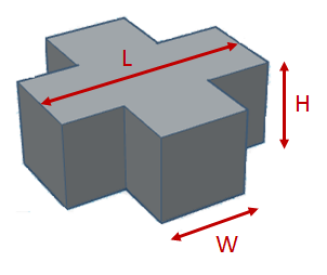
The schematic of the silicon cross resonator is shown in Fig. 1a. Silicon is chosen due to its high relative permittivity of and its low loss nature in the terahertz regime. The width, height and lattice constant of the cross are fixed at 70m, 150 m and 500 m respectively. These dimensions are optimized to excite electric and magnetic resonances at the desired range of frequencies. We used the FDTD method to perform simulations, with a linearly polarized plane wave incident normally on the metasurface with its electric field in direction and propagating in direction.
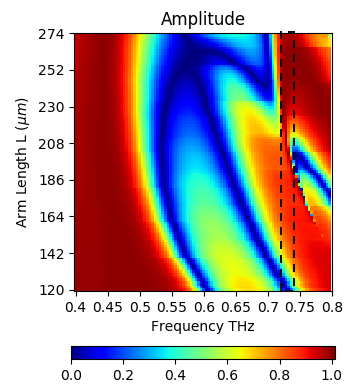
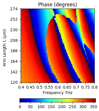
Due to the subwavelength spacing of the resonators and low coupling between adjacent resonators we considered the electromagnetic response of one resonator by replicating it as an infinite array in and directions achieved by the periodic boundary condition. Each resonator can support electric and magnetic resonance when the dimensions become comparable to the wavelength of the incident light [20]. High transmission can be achieved by tuning the dimensions such that the two resonance overlap spectrally and cancel out the back scattered light. Figure 1b and 1c show the transmission amplitude and phase respectively as a function of the arm length varied from 120-275 m and frequency 0.4-0.8 THz. From the simulation data we have selected eight resonators with nearly equal phase steps of to cover full range.
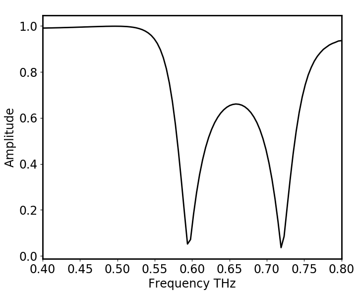
The amplitude and phase of the transmitted light is computed by using design parameters. Figure 2a and 2b shows the typical amplitude and phase response across the desired frequency range 0.4-0.8 THz for a cross arm length of m.
3 Vortex beam generator
As an application, we propose a metasurface vortex beam generator at terahertz frequencies. The phase function of the vortex generator is given by a spiraling function as the following equation:
| (1) |
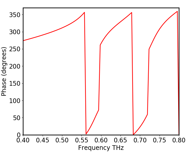
where () are the coordinates in the metasurface plane. The continuous phase profile of the vortex generator given in the Eq. 1 is discretized to eight phase levels and the corresponding eight cross resonators dimensions are given in Table 1. The transmission phase curve is shown in Fig. 3. It is revealed that all the resonators are showing high transmission with a mean variation of 5%.
| Arm Length (m) | 187 | 201 | 208 | 212 | 217 | 225 | 237 | 267 |
|---|---|---|---|---|---|---|---|---|
| Amplitude | 0.87 | 0.88 | 0.97 | 0.99 | 0.98 | 0.95 | 0.99 | 0.99 |
| Phase | 2 | 42 | 90 | 135 | 183 | 228 | 271 | 317 |


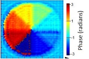
We designed a spatial phase element with a diameter 1.2 cm consisting of eight types of cross resonators in corresponding eight octants as shown in Fig. 4a. Such optical element has dimensions useful for range of applications in THz experiments including synchrotron beamlines. The FDTD simulated transmission the phase is shown in Fig. 4b. The designed spiraling phase was indeed following the required azimuthal span.
3.1 Fabrication
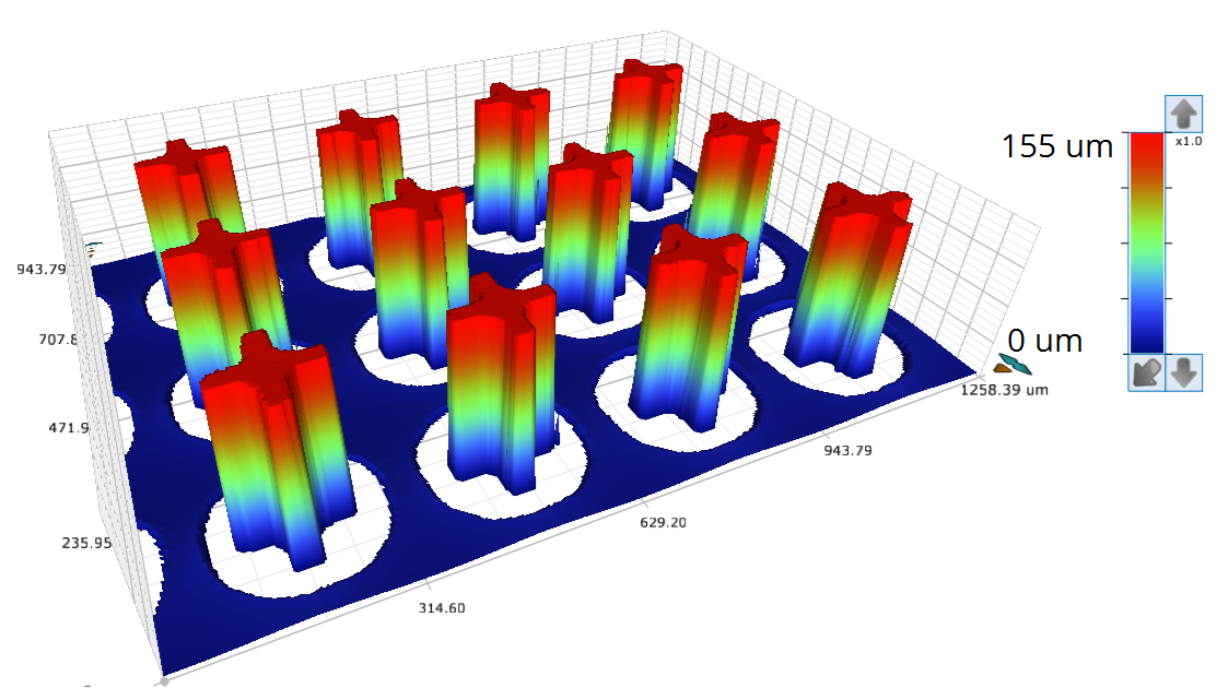
A silicon wafer of standard 500 m thickness was used for the fabrication of the optical meta-surface element. The device was fabricated using photolithography followed by reactive ion etching (RIE). The mask for the photolithography was fabricated using the Intelligent micropatterning SF100 XPRESS direct writing system. We used AZ4562 photo-resist in order to obtain thicker resist coating. The large thickness was needed to obtain a high etch depth of 150 m by RIE (the resist was a acting as a sacrificial mask). The standard Bosh process was used to etch silicon for the required high aspect ratio pattern. A photograph of the fabricated metadevice and the optical profilometer measurement are shown in Fig. 5a and 5b. The required depth of 150 m was achieved after 90 min plasma etching.

4 Conclusions and outlook
In this work, we have shown that appropriate choice of the dimensions of the cross resonator can achieve spectral overlap of the electric and magnetic resonances thus providing full 2 phase coverage and high transmission amplitudes. We have employed eight types of cross resonators as building blocks to construct a spiraling phase plate with eight discretized phase levels. FDTD simulation results clearly show the eight discrete phase levels across the surface of the meta-surface optical element. There was a 12% difference in the transmission amplitudes across the eight resonators observed. The metadevice was fabricated using standard projection micro-lithography and plasma etching.
Such simple-to-fabricate optical elements are promising for the phase and polarisation control at the IR-THz beamline at the Australian Synchrotron. Applications in opto-mechanics also require high-transmission optical elements for imparting torque onto absorbing and scattering objects. The demonstrated simple fabrication method is applicable to a wider range of optical elements such as conical lenses (axicons), and gratings and can deliver higher quality surface finish as compared with 3D printing recently used for THz polarisation optics [21]. Optical elements for spin and orbital angular momentum control are expected to provide new insights into complex secondary structures of polymers including bio-polymers such as silk which have strong signatures at IR-THz spectral range [22, 23, 24, 25].
Acknowledgements
This work was performed in part at the Melbourne Centre for Nanofabrication (MCN) in the Victorian Node of the Australian National Fabrication Facility (ANFF).
References
- [1] Yu, N. and Capasso, F., “Flat optics with designer metasurfaces,” Nature materials 13(2), 139–150 (2014).
- [2] Genevet, P., Capasso, F., Aieta, F., Khorasaninejad, M., and Devlin, R., “Recent advances in planar optics: from plasmonic to dielectric metasurfaces,” Optica 4(1), 139–152 (2017).
- [3] Sautter, J., Staude, I., Decker, M., Rusak, E., Neshev, D. N., Brener, I., and Kivshar, Y. S., “Active tuning of all-dielectric metasurfaces,” ACS nano 9(4), 4308–4315 (2015).
- [4] Chen, H.-T., Taylor, A. J., and Yu, N., “A review of metasurfaces: physics and applications,” Reports on Progress in Physics 79(7), 076401 (2016).
- [5] Yu, Y. F., Zhu, A. Y., Paniagua-Domínguez, R., Fu, Y. H., Luk’yanchuk, B., and Kuznetsov, A. I., “High-transmission dielectric metasurface with 2 phase control at visible wavelengths,” Laser & Photonics Reviews 9(4), 412–418 (2015).
- [6] Arbabi, A., Horie, Y., Bagheri, M., and Faraon, A., “Dielectric metasurfaces for complete control of phase and polarization with subwavelength spatial resolution and high transmission,” Nature nanotechnology 10(11), 937–943 (2015).
- [7] Kildishev, A. V., Boltasseva, A., and Shalaev, V. M., “Planar photonics with metasurfaces,” Science 339(6125), 1232009 (2013).
- [8] Chong, K. E., Staude, I., James, A., Dominguez, J., Liu, S., Campione, S., Subramania, G. S., Luk, T. S., Decker, M., Neshev, D. N., et al., “Polarization-independent silicon metadevices for efficient optical wavefront control,” Nano letters 15(8), 5369–5374 (2015).
- [9] Khorasaninejad, M., Chen, W. T., Devlin, R. C., Oh, J., Zhu, A. Y., and Capasso, F., “Metalenses at visible wavelengths: Diffraction-limited focusing and subwavelength resolution imaging,” Science 352(6290), 1190–1194 (2016).
- [10] Cheng, J., Ansari-Oghol-Beig, D., and Mosallaei, H., “Wave manipulation with designer dielectric metasurfaces,” Optics letters 39(21), 6285–6288 (2014).
- [11] Genevet, P. and Capasso, F., “Holographic optical metasurfaces: a review of current progress,” Reports on Progress in Physics 78(2), 024401 (2015).
- [12] Yang, Y., Wang, W., Moitra, P., Kravchenko, I. I., Briggs, D. P., and Valentine, J., “Dielectric meta-reflectarray for broadband linear polarization conversion and optical vortex generation,” Nano letters 14(3), 1394–1399 (2014).
- [13] Khorasaninejad, M., Zhu, W., and Crozier, K., “Efficient polarization beam splitter pixels based on a dielectric metasurface,” Optica 2(4), 376–382 (2015).
- [14] Chang, C.-C., Headland, D., Abbott, D., Withayachumnankul, W., and Chen, H.-T., “Demonstration of a highly efficient terahertz flat lens employing tri-layer metasurfaces,” Optics Letters 42(9), 1867–1870 (2017).
- [15] Wang, Q., Zhang, X., Xu, Y., Tian, Z., Gu, J., Yue, W., Zhang, S., Han, J., and Zhang, W., “A broadband metasurface-based terahertz flat-lens array,” Advanced Optical Materials 3(6), 779–785 (2015).
- [16] Niu, T., Withayachumnankul, W., Ung, B. S.-Y., Menekse, H., Bhaskaran, M., Sriram, S., and Fumeaux, C., “Experimental demonstration of reflectarray antennas at terahertz frequencies,” Optics express 21(3), 2875–2889 (2013).
- [17] Cong, L., Xu, N., Gu, J., Singh, R., Han, J., and Zhang, W., “Highly flexible broadband terahertz metamaterial quarter-wave plate,” Laser & Photonics Reviews 8(4), 626–632 (2014).
- [18] Wang, D., Gu, Y., Gong, Y., Qiu, C.-W., and Hong, M., “An ultrathin terahertz quarter-wave plate using planar babinet-inverted metasurface,” Optics express 23(9), 11114–11122 (2015).
- [19] Ma, Z., Hanham, S. M., Albella, P., Ng, B., Lu, H. T., Gong, Y., Maier, S. A., and Hong, M., “Terahertz all-dielectric magnetic mirror metasurfaces,” ACS Photonics 3(6), 1010–1018 (2016).
- [20] Evlyukhin, A. B., Reinhardt, C., Seidel, A., Luk’yanchuk, B. S., and Chichkov, B. N., “Optical response features of si-nanoparticle arrays,” Physical Review B 82(4), 045404 (2010).
- [21] Ryu, M., Linklater, D. P., Hart, W., Balčytis, A., Skliutas, E., Malinauskas, M., Appadoo, D., Tan, Y.-R. E., Ivanova, E. P., Morikawa, J., and Juodkazis, S., “3D printed polarising grids for IR-THz synchrotron radiation,” J. Optics , (provisionally accepted) (2017).
- [22] Balčytis, A., Ryu, M., Wang, X., Novelli, F., Seniutinas, G., Du, S., Wang, X., Li, J., Davis, J., Appadoo, D., Morikawa, J., and Juodkazis, S., “Silk: Optical properties over 12.6 octaves THz-IR-Visible-UV range,” Materials 10(4), 356 (2017).
- [23] Ryu, M., Balčytis, A., Wang, X., Vongsvivut, J., Hikima, Y., Li, J., Tobin, M. J., Juodkazis, S., and Morikawa, J., “Orientational mapping augmented sub-wavelength hyper-spectral imaging of silk,” Sci. Reports 7, 7419 (2017).
- [24] Morikawa, J., Ryu, M., Balčytis, A., Seniutinas, G., Fan, L., Mizeikis, V., Li, J. L., Wang, X. W., Zamengo, M., Wang, X., and Juodkazis, S., “Silk fibroin as water-soluble bio-resist and its thermal properties,” RSC Advances 6, 11863 – 11869 (2015).
- [25] Ryu, M., Kobayashi, H., Balčytis, A., Wang, X., Vongsvivut, J., Li, J., Urayama, N., Mizeikis, V., Tobin, M., Juodkazis, S., and Morikawa, J., “Nanoscale chemical mapping of laser-solubilized silk,” Materials Research Express 4(11), 115028 (2017).