Electrical tuning of spin splitting in Bi-doped ZnO nanowires
Abstract
Published version available at https://doi.org/10.1103/PhysRevB.97.035405
The effect of applying an external electric field on doping-induced spin-orbit splitting of the lowest conduction-band states in a bismuth-doped zinc oxide nanowire is studied by performing electronic structure calculations within the framework of density functional theory. It is demonstrated that spin splitting in Bi-doped ZnO nanowires could be tuned and enhanced electrically via control of the strength and direction of the applied electric field, thanks to the non-uniform and anisotropic response of the ZnO:Bi nanowire to external electric fields. The results reported here indicate that a single ZnO nanowire doped with a low concentration of Bi could function as a spintronic device, operation of which is controlled by applied lateral electric fields.
In the presence of noncentrosymmetric electric fields, the spin-orbit (SO) interaction leads to a -dependent splitting of electronic states, enabling electrical control of the spin-split states in spintronic devices Rashba and Efros (2003); Sahoo et al. (2005); Nowack et al. (2007). The development of a class of spintronic materials is thus facilitated by engineering (or exploiting) inversion asymmetries to generate intrinsic electric fields Ishizaka et al. (2011); Di Sante et al. (2013); Liu et al. (2013); Güler-Kılıç and Ç. Kılıç (2015); Cheng et al. (2016) as well as devising architectures in which external electric fields are used Nitta et al. (1997); Liang and Gao (2012); Gong et al. (2013). It has recently been proposed that surface deposition Calleja et al. (2015) and doping Aras et al. (2017) with heavy elements could also be used to develop materials with spintronic functionalities. In particular, the predictions of Ref. Aras et al., 2017 show that doping a light semiconducting (ZnO) nanowire with a heavy element (Bi) leads to linear-in- splitting of the conduction-band (CB) states through SO interaction. It is thus anticipated that a single ZnO nanowire doped with a low concentration of Bi could function as a spintronic device. The objective of the present paper is to investigate if the spintronic properties of a ZnO:Bi nanowire could be tuned or enhanced electrically. In our previous paperAras et al. (2017), we showed that the -dependent SO splitting in ZnO:Bi nanowires could be tuned by adjusting the dopant concentration. Here we demonstrate that applying external electric fields provides an effective means to enhance the linear-in- SO splitting of the CB states in ZnO:Bi nanowires. We find that the SO splitting energy could be made to have a superlinear increase with increasing electric field strength , which is mediated by controlling the direction of the applied electric field . This is found to be facilitated by the non-uniform and anisotropic response of the ZnO:Bi nanowire to external electric fields. The latter remind the (converse) piezoelectric response of undoped ZnO nanowires He et al. ; Agrawal and Espinosa (2011); Broitman et al. (2013) and microbelts Hu et al. (2009). On the other hand, our results also indicate that the presence of the substitutional Bi dopant on the ZnO nanowire surface reduces the amount of deformation of the nanowire under an electric field.
As long as single Co-doped ZnO nanowires and nanorods have been produced and characterized Liang et al. (2009); Segura-Ruiz et al. (2011); Ko et al. (2012), we think that the realization of a single ZnO:Bi nanowire is not beyond the reach of current capabilities, although differences between cobalt and bismuth (e.g., bismuth’s larger ionic radius Shannon and Prewitt (1969) and lower solubility Smith et al. (1989) in bulk ZnO) should be taken into consideration. Since experimental studies on single Bi-doped ZnO nanowires were not available (to our knowledge), the realization and stability of a single ZnO:Bi nanowire were examined theoretically in our previous publications Kılıç et al. (2016); Aras et al. (2017) with the aid of defect calculations and finite-temperature ab initio molecular dynamics simulations, as will be discussed in the Appendix.
The findings reported here were obtained via electronic structure calculations performed within framework of the density functional theory (DFT) by employing periodic supercells. Although the supercells were in practice subject to the Bloch periodicity condition in all directions, the supercell dimensions perpendicular to the nanowire axis were set to be significantly larger than the nanowire diameter in order to create a vacuum region (of thickness larger than 15 Å) that avoid interactions between the nanowire and its periodic images. We used the Vienna ab initio simulation package Kresse and Furthmüller (1996) (VASP) together with its projected-augmented-wave potential database Kresse and Joubert (1999), adopting the rotationally-invariant DFT+ approach Dudarev et al. (1998) in combination with the Perdew-Burke-Ernzerhof exchange-correlation functional Perdew et al. (1996), and taking the SO coupling into account as implemented Hobbs et al. (2000); Steiner et al. (2016) in the VASP code. The 2 and 2, 3 and 4, and 6 and 6 states were treated as valence states for oxygen, zinc, and bismuth, respectively. Plane wave basis sets with a kinetic energy cutoff of 400 eV were used to represent the electronic states. In test calculations Aras et al. (2017) the kinetic energy cutoff was increased by 10 % and the change in the SO splitting energies turned out to be smaller than 0.5 %. The value of Hubbard was set to 7.7 eV Kılıç et al. (2016), which was applied to the Zn 3 states. The DFT+ approach was preferred over the standard (semilocal) DFT calculations in order to reduce the underestimation of the state binding energies Aras and Ç. Kılıç (2014). We applied lateral electric fields in the or directions of varying strength (from 0.1 to 0.5 eV/Å with an increment of 0.1 eV/Å), orienting the nanowire axis along the direction. It should be reminded that VASP handles the external electric fields by introducing artificial dipole sheets in the middle of the vacuum regions in the supercell, cf. Ref. Feibelman, 2001. Structural optimizations were performed for each atomic configuration, separately for each given , by minimizing the total energy until the maximum value of residual forces on atoms was reduced to be smaller than eV/Å, using the -point for sampling the supercell Brillouin zone (BZ). We determined Aras et al. (2017) an error bar of 0.2 meV for the energy per ZnO unit owing to the BZ sampling achieved through zone folding. Convergence criterion for the electronic self-consistency was set up to 10-6 eV and 10-8 eV in structural optimizations and electronic structure calculations, respectively.
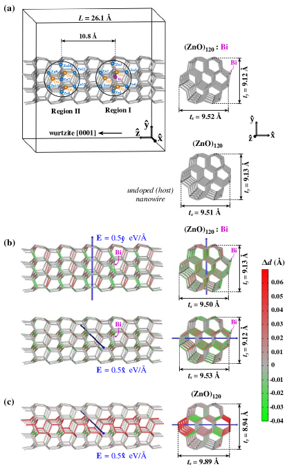
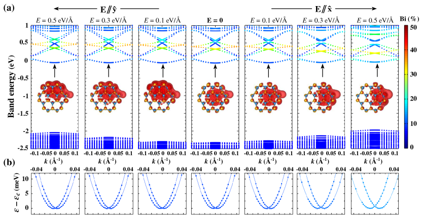
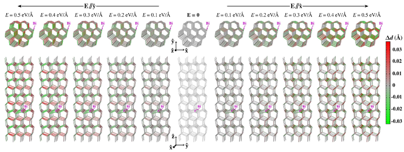
Figure 1(a) shows the equilibrium atomic configuration for a Bi-doped ZnO nanowire in the absence of an external electric field, where the Bi dopant substitutes Zn at a surface site of the host ZnO nanowire. We refer to the Appendix for a discussion of issues concerning the realization of this configuration. The equilibrium atomic configuration for the undoped (host) nanowire is also shown in Fig. 1(a), which was used in former theoretical studies by others (e.g., Refs. Fan et al., 2007; Agrawal and Espinosa, 2011) as well as the authors Kılıç et al. (2016); Aras et al. (2017). The wire thicknesses and are indicated in Fig. 1(a) for both the doped and undoped nanowires. Comparing these thicknesses, it is clear that the incorporation of Bi causes insignificant deformation in the wire morphology, which means that the accommodation of Bi induces mostly local relaxations. It should also be pointed out that the host nanowire’s thickness is smaller than the experimental diameter () values measured for high-aspect-ratio ZnO nanorods with nm Yin et al. (2004) and thin ZnO nanowires with nm Stichtenoth et al. (2007). The variation of the results with respect to the nanowire’s thickness was studied in Ref. Aras et al., 2017 (in the absence of an external electric field), which will not be done here.
The equilibrium configurations in the presence of electric fields are given in Figs. 1(b) and S1 (see Ref. sup, ). Since the electric-field-induced changes in the atomic positions are not visible in the scale of the figures, the sticks representing the Zn-O bonds are colored to reflect the electric-field-induced changes in the bond lengths. Hence, the structural response of the ZnO:Bi nanowire to the applied electric fields could be inferred from the distributions of red and green sticks (representing the elongated and shrunk bonds, respectively). It is clear in Figs. 1(b) and S1 (see Ref. sup, ) that the electric-field-induced structural changes occur all around the nanowire. Nevertheless, a comparison between the bond lengths in Regions I and II depicted in Fig. 1(a), the values of which are provided in Table S1 (see Ref. sup, ), reveals that the structural changes are more pronounced in the vicinity of the dopant. For example, the O1Bi (O2Bi) bond located in Region I exhibits the greatest shrinkage for (), the degree of which is proportional to . The respective bonds in Region II (far from the dopant), i.e., the O4Zn7 and O5Zn7 bonds, however exhibit considerably smaller shrinkage.
As mentioned above, the presence of the Bi dopant on the ZnO nanowire surface reduces the amount of deformation in the wire morphology under a lateral electric field. This could be seen by comparing the structures in Figs. 1(b) and (c). For the doped nanowire, the and values in Fig. 1(b) are little different from those in Fig. 1(a). In contrast, there is a significant increase (decrease) in the () of the undoped nanowire as a result of applying eV/Å, yielding a noticeable modification in the wire cross-section since the ratio changes from 1.04 to 1.11. The distribution of the stretched (shrunk) bonds, cf. red (green) sticks, in Fig. 1(c) is also noticeably different than that in Fig. 1(b), which reveals the microscopic origin of the increase (decrease) in (). It should be noticed that applying a lateral electric field make the Zn-O bonds that are aligned with the wire axis elongate according to our prediction, which is in accordance with the response of a ZnO microbelt Hu et al. (2009) to an applied electric field perpendicular to its -axis.
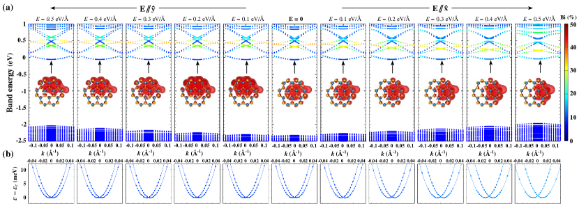
The electronic energy bands of the (ZnO)120:Bi nanowire, calculated for 0.5, 0.4, 0.3, 0.2, 0.1, , 0.1, 0.2, 0.3, 0.4, and 0.5 eV/Å, are shown in Figs. 2(a) and S2(a) (see Ref. sup, ) where the symbols are colored to reflect the percent contribution from Bi to the electronic states. The coloring is accomplished by computing the contributions from the Zn, O, and Bi atoms that are obtained by projecting the state wave functions onto spherical harmonics within a sphere around each atom. The vertical arrows point to the conduction-band minimum (CBM) that occurs at . It is seen that Bi-derived states occur as resonances in the conduction band, energies of which get lowered (remain roughly constant) for (). The CBM state charge density is noticeably distorted in a directed manner as imposed by the direction of the applied electric field , which is inferred from the isosurfaces given as insets in Fig. 2(a). Whereas Bi contribution to the CBM wave function decreases slowly with for , applying in the direction makes the CBM wave function have a higher contribution from Bi, in proportionality with . Thus an important effect of applying an external electric field is to vary the Bi contribution to the lower CB states.
Figures 2(b) and S2(b) (see Ref. sup, ) display close-up views of the two lowest (spin-split) conduction bands, where the bands are shifted by subtracting the lowest eigenvalue of the conduction band from the band energies . These bands are partially occupied since the aforementioned Bi-derived resonant states in the conduction band are empty, reflecting the donor behavior of Bi in ZnO nanowires Kılıç et al. (2016). The dispersion of the spin-split bands in Fig. 2(b) is accurately described by
| (1) |
represented by the solid curves in each panel. Although Eq. (1) is of the same form of the Bychkov-Rashba expression Bychkov and Rashba (1984), the electrons filling the bands do not form a two-dimensional electron gas, as seen from the insets of Figs. 2(a) and S2(a) (see Ref. sup, ). The latter applies to the case of zero electric field, as discussed in detail in Ref. Aras et al., 2017. It is clear that the splitting energy increases (decreases slowly) as increases for (). This is the same trend for the Bi contribution to the CBM wave function, as noted in the preceding paragraph. Accordingly the variations of and the Bi contribution to with follow the same trend, as seen in Figs. 3(a) and 3(b). This means that increasing the Bi contribution to the lower CB states leads to the enhancement of spin-orbit splitting of those states. It should also be pointed out that induces a much smaller splitting in the undoped nanowire owing to the absence of the Bi contribution. This is illustrated in Fig. S3 (see Ref. sup, ) where the linear coefficient eVÅ in the absence of the heavy element Bi, which should be compared to the respective value of eVÅ in the presence of the Bi dopant.

The splitting energy plotted in Fig. 3(a) is given by according to Eq.(1). Thus the variation of the linear coefficient and the momentum offset with is studied in Figs. 3(c) and 3(d), respectively, where the black curves represent the parameterization according to
| (2) | |||||
| (3) |
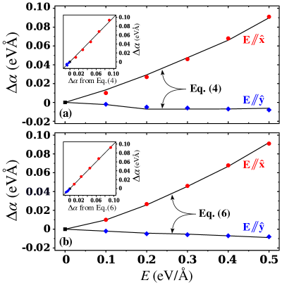
Here the units of , and are eVÅ, Å-1 and eV/Å, respectively; eVÅ and Å-1 are the values of the linear coefficient and the momentum offset, respectively, in the absence of an external electric field. It is noteworthy that and are both substantially enhanced with increasing in the case of , which exhibit a slight decrease for . The variation of with is seemingly superlinear for . It is also notable that the (ZnO)120:Bi nanowire has an anisotropic response to the external electric fields as regards the degree of SO splitting of CB states. Thus, in an experimental setup, it would be necessary first to determine the electric field directions for which and show increasing and decreasing variations with increasing . This would enable directional control of the spin-split states in a practical application.
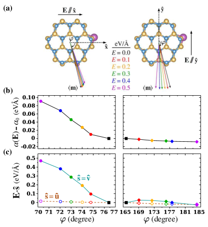
From a fundamental physics point of view, the linear coefficient introduced in Eq. (1) is related to the expectation value of the SO interaction operator with , which could be approximated Aras et al. (2017) as where and denote the expectation values of the magnetization density and the operator , respectively. A linear dependence of on would therefore be expected. Hence the nonlinear variation with the applied electric field in Fig. 3(c) deserves further investigation. To this aim, the variation of with will be analyzed in terms of -induced changes in and . Note that not only but also varies with in our noncollinear DFT calculations where is determined self-consistently, as shown in Fig. 4(a) where denotes the angle between and . The computed values for the magnitude of are given in Table S2 (see Ref. sup, ). It should also be remarked that the projections of the vector perpendicular (parallel) to the vector make nonzero (zero) contributions to , and therefore to the splitting energy. It is thus convenient to use an intrinsic coordinate system defined by the orthogonal unit vectors , and satisfying and , which could be taken as , , and , where and denote the angles between and and and , respectively. For the vectors in Fig. 4(a), the angle pairs (, ) take the values given in Table S2 (see Ref. sup, ). It is important to notice that the electric-field-induced change in arising only from the projections with yields a nonzero contribution to . It is thus instructive to explore the relationship between -induced variation of , i.e., , and the projections with and as well as the -induced change in , which will be denoted as . A comparative inspection of Figs. 4(b) and 4(c) reveals that the variation of with respect to is of the same trend as that of () for (). In view of this and the foregoing discussion, a fitting according to
| (4) |
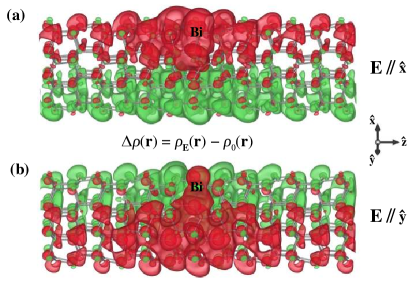
was performed, where denotes the unit vector in the direction of in the absence of the external electric field. We found that the result of this fitting is not entirely satisfactory, which was inferred from Fig. 5(a). We attribute the latter to the fact that the non-uniform response of the nanowire to the applied electric field is not taken into account in Eq.(4), which is demonstrated by the graphs of the -induced change in the CBM state charge density in Fig. 6. The projections in Eq.(4) are thus replaced by the integrals
| (5) |
with or , resulting in
| (6) |
In Eq.(5), denotes the electric-field-induced change in the self-consistent potential . Note that for a uniform electric field within a non-self-consistent description. The fitting according to Eq.(6) yields Å2, Å2, and eVÅ/, the result of which is quite satisfactory as seen in Fig. 5(b). The values obtained from the right-hand-side (RHS) of Eq.(6) are given in the second column of Table 1, which should be compared to the original values in the first column of the same table. The contributions from the three terms in the RHS of Eq.(6) are given in the third, fourth, and fifth columns of Table 1. It is noticeable that the and terms have the greatest contribution to for and , respectively, although the term has also a non-negligible contribution. Since both and are positive, a decrease in occurs owing to when . On the other hand, an increase in occurs when and/or . Hence the increasing and decreasing variation of with is traced to the sign of the ( and ) integrals, which is practically the same as the sign of . Accordingly, as long as the directions and could not be determined a priori, the direction of the applied electric field must be chosen carefully to ensure that an electric-field-induced increase in is achieved. The latter would facilitate the directional control of the spin-split CB states, as also mentioned above, which would likely involve trial-and-error in a practical application. It is nonetheless remarkable that a single ZnO:Bi nanowire such as studied here could function as a spintronic device, operation of which is controlled by applying lateral electric fields.
| RHS of Eq.(6) | ||||
|---|---|---|---|---|
In summary, the results of our density-functional calculations show that doping-induced linear-in- spin splitting of the lowest conduction-band states in a Bi-doped ZnO nanowire could be tuned by applying lateral electric fields via control of the electric field strength and direction. We find that the degree of this splitting could be made to have a superlinear increase with increasing electric field strength, which is mediated by controlling the electric field direction. Our analysis reveals that this is facilitated by the non-uniform and anisotropic response of the ZnO:Bi nanowire to the applied electric field. These findings indicate that a single ZnO nanowire doped with a low concentration of Bi could function as a spintronic device, operation of which is controlled electrically.
The authors acknowledge financial support from the Scientific and Technological Research Council of Turkey (TUBITAK) through Grant No. 114F155. The calculations reported were carried out at the High Performance and Grid Computing Center (TRUBA Resources) of TUBITAK ULAKBIM.
*
Appendix A Bi defects in the ZnO:Bi nanowire
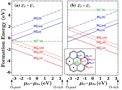
We have recently conducted Kılıç et al. (2016) a theoretical characterization of a Bi-doped ZnO nanowire in a site-specific manner as regards the location and charge-state of the dopant, by calculating the defect formation energy for a number of extrinsic defects formed via the incorporation of Bi into the Zn, O or interstitial () sites in the bulk-like (), surface () or subsurface () regions of the nanowire. It is to be emphasized that is an indicator for the abundance of the defect under given thermodynamic conditions since it is a significant portion of the Gibbs energy of formation that determines the equilibrium defect concentration. The defects considered are shown in the inset of Fig. 7, which are denoted as , , , , , , . In structural optimizations, placing Bi initially at either of the unlabeled sites shown in the inset of Fig. 7 resulted in an unstable configuration in which the nanowire is damaged. These two unstable configurations are discarded. In the present paper, the doping configuration displayed in Fig. 1(a) contains the defect . We studied the formation energies of the foregoing defects as a function of the Fermi level and the atomic chemical potentials , and . Our investigations Kılıç et al. (2016); Aras et al. (2017) indicate that this doping configuration can be realized under reasonable thermodynamic conditions, which will be summarized here with the aid of the plots of versus the difference . The latter are given in Figs. 7(a) and 7(b) for two limiting values of . The value of is set to the adsorption energy of a Bi atom on the nanowire surface, cf. Ref. Aras et al., 2017. It is seen in Figs. 7(a) and 7(b) that the defect in a charge state 0 or (depending on the location of the Fermi level) has not only lowest but also negative formation energies for a wide range of thermodynamic conditions. The only exception to this is that has a lower formation energy under O-poor conditions for in a narrow range of . Clearly, the formation of , rather than the rest of the alternatives with higher formation energies, could be favored by adjusting thermodynamic conditions (i.e., by avoiding the values of and corresponding to the latter range of ). This means that the doping configuration displayed in Fig. 1(a) could be realized under controlled thermodynamic conditions. Besides, ab initio molecular dynamics simulations performed at high temperature indicate that the same degree of stability could be assigned to the undoped ZnO and doped ZnO:Bi nanowires Aras et al. (2017). Finally, we think that the synthesis of surface-doped ZnO:Bi nanowire studied here would benefit from the low solubility of Bi in ZnO that derives the segregation of Bi in ZnO varistors Smith et al. (1989); Kobayashi et al. (1998). A segregation tendency is also revealed for Bi in ZnO nanowires in Figs. 7(a) and 7(b) where the surface () defects have lower formation energies compared to the respective bulk-like () and subsurface () defects.
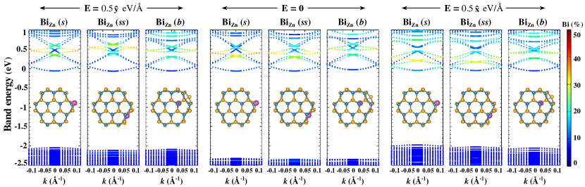
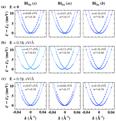
Since the formation energy of is significantly lower than that of and , cf. Figs. 7(a) and 7(b), the equilibrium concentration of would be several orders of magnitude higher than that of and at room temperature. It is nevertheless interesting to see if spin splitting of the CB states occurs also for and . Figures 8(a)-(c) show the SO-split conduction bands for ZnO:Bi nanowires containing , , and for , , and eV/Å. An expanded view of the band structures are provided in Fig. S4 (see Ref. sup, ) where the optimized atomic structures are included as insets. Note that spin-orbit splitting of the CB states is present in each panel of Fig. 8. Moreover, the linear coefficient takes quite similar values for , and . On the other hand, for does not show much variation with . The latter implies that electrical control of doping-induced spin splitting explored here could be achieved only in the case of surface (as opposed to bulk) doping of ZnO nanowires with Bi.
References
- Rashba and Efros (2003) E. I. Rashba and A. L. Efros, Phys. Rev. Lett. 91, 126405 (2003).
- Sahoo et al. (2005) S. Sahoo, T. Kontos, J. Furer, C. Hoffmann, M. Graber, A. Cottet, and C. Schonenberger, Nat. Phys. 1, 99 (2005).
- Nowack et al. (2007) K. C. Nowack, F. H. L. Koppens, Y. V. Nazarov, and L. M. K. Vandersypen, Science 318, 1430 (2007).
- Ishizaka et al. (2011) K. Ishizaka, M. S. Bahramy, H. Murakawa, M. Sakano, T. Shimojima, T. Sonobe, K. Koizumi, S. Shin, H. Miyahara, A. Kimura, K. Miyamoto, T. Okuda, H. Namatame, R. Taniguchi, M. amd Arita, N. Nagaosa, K. Kobayashi, Y. Murakami, R. Kumai, Y. Kaneko, Y. Onose, and Y. Tokura, Nat. Mater. 10, 521 (2011).
- Di Sante et al. (2013) D. Di Sante, P. Barone, R. Bertacco, and S. Picozzi, Adv. Mater. 25, 509 (2013).
- Liu et al. (2013) Q. Liu, Y. Guo, and A. J. Freeman, Nano Lett. 13, 5264 (2013).
- Güler-Kılıç and Ç. Kılıç (2015) S. Güler-Kılıç and Ç. Kılıç, Phys. Rev. B 91, 245204 (2015).
- Cheng et al. (2016) C. Cheng, J.-T. Sun, X.-R. Chen, H.-X. Fu, and S. Meng, Nanoscale 8, 17854 (2016).
- Nitta et al. (1997) J. Nitta, T. Akazaki, H. Takayanagi, and T. Enoki, Phys. Rev. Lett. 78, 1335 (1997).
- Liang and Gao (2012) D. Liang and X. P. Gao, Nano Lett. 12, 3263 (2012).
- Gong et al. (2013) S.-J. Gong, C.-G. Duan, Y. Zhu, Z.-Q. Zhu, and J.-H. Chu, Phys. Rev. B 87, 035403 (2013).
- Calleja et al. (2015) F. Calleja, H. Ochoa, M. Garnica, S. Barja, J. J. Navarro, A. Black, M. M. Otrokov, E. V. Chulkov, A. Arnau, A. L. Vazquez de Parga, F. Guinea, and R. Miranda, Nat. Phys. 11, 43 (2015).
- Aras et al. (2017) M. Aras, S. Güler-Kılıç, and Ç. Kılıç, Phys. Rev. B 95, 155404 (2017).
- (14) J. H. He, C. L. Hsin, J. Liu, L. J. Chen, and Z. L. Wang, Adv. Mater. 19, 781.
- Agrawal and Espinosa (2011) R. Agrawal and H. D. Espinosa, Nano Lett. 11, 786 (2011).
- Broitman et al. (2013) E. Broitman, M. Y. Soomro, J. Lu, M. Willander, and L. Hultman, Phys. Chem. Chem. Phys. 15, 11113 (2013).
- Hu et al. (2009) Y. Hu, Y. Gao, S. Singamaneni, V. V. Tsukruk, and Z. L. Wang, Nano Lett. 9, 2661 (2009).
- Liang et al. (2009) W. Liang, B. D. Yuhas, and P. Yang, Nano Lett. 9, 892 (2009).
- Segura-Ruiz et al. (2011) J. Segura-Ruiz, G. Mart nez-Criado, M. H. Chu, S. Geburt, and C. Ronning, Nano Lett. 11, 5322 (2011).
- Ko et al. (2012) T. Y. Ko, M.-H. Tsai, C.-S. Lee, and K. W. Sun, J. Nanopart. Res. 14, 1253 (2012).
- Shannon and Prewitt (1969) R. D. Shannon and C. T. Prewitt, Acta Cryst. B 25, 925 (1969).
- Smith et al. (1989) A. Smith, J.-F. Baumard, P. Abelard, and M.-F. Denanot, J. Appl. Phys. 65, 5119 (1989).
- Kılıç et al. (2016) Ç. Kılıç, M. Aras, and S. Güler-Kılıç, “Computational studies of bismuth-doped zinc oxide nanowires,” in Low-Dimensional and Nanostructured Materials and Devices: Properties, Synthesis, Characterization, Modelling and Applications, edited by H. Ünlü, M. N. J. Horing, and J. Dabowski (Springer International Publishing, Cham, 2016) pp. 401–421.
- Kresse and Furthmüller (1996) G. Kresse and J. Furthmüller, Phys. Rev. B 54, 11169 (1996).
- Kresse and Joubert (1999) G. Kresse and D. Joubert, Phys. Rev. B 59, 1758 (1999).
- Dudarev et al. (1998) S. L. Dudarev, G. A. Botton, S. Y. Savrasov, C. J. Humphreys, and A. P. Sutton, Phys. Rev. B 57, 1505 (1998).
- Perdew et al. (1996) J. P. Perdew, K. Burke, and M. Ernzerhof, Phys. Rev. Lett. 77, 3865 (1996).
- Hobbs et al. (2000) D. Hobbs, G. Kresse, and J. Hafner, Phys. Rev. B 62, 11556 (2000).
- Steiner et al. (2016) S. Steiner, S. Khmelevskyi, M. Marsmann, and G. Kresse, Phys. Rev. B 93, 224425 (2016).
- Aras and Ç. Kılıç (2014) M. Aras and Ç. Kılıç, J. Chem. Phys. 141, 044106 (2014).
- Feibelman (2001) P. J. Feibelman, Phys. Rev. B 64, 125403 (2001).
- Fan et al. (2007) W. Fan, H. Xu, A. L. Rosa, T. Frauenheim, and R. Q. Zhang, Phys. Rev. B 76, 073302 (2007).
- Yin et al. (2004) M. Yin, Y. Gu, I. L. Kuskovsky, T. Andelman, Y. Zhu, G. F. Neumark, and S. O’Brien, J. Am. Chem. Soc. 126, 6206 (2004).
- Stichtenoth et al. (2007) D. Stichtenoth, C. Ronning, T. Niermann, L. Wischmeier, T. Voss, C.-J. Chien, P.-C. Chang, and J. G. Lu, Nanotechnology 18, 435701 (2007).
- (35) See Supplemental Material at for (i) Fig. S1 that displays the equilibrium atomic configuration for the ZnO:Bi nanowire under the applied electric fields, (ii) Table S1 that lists the electric-field-induced changes in the lengths of the bonds in Regions I and II depicted in Fig. 1(a), (iii) Fig. S2 that supplements Fig. 2, (vi) Fig. S3 displaying the electronic energy bands of the undoped ZnO nanowire for and eV/Å, (v) Table S2 that lists the values for the magnitute and angles of the vectors depicted in Fig. 4(a), (vi) Fig. S4 that displays the electronic energy bands of ZnO:Bi nanowires containing substitutional defects , , and for , , and eV/Å.
- Bychkov and Rashba (1984) Y. A. Bychkov and E. I. Rashba, JETP Lett. 39, 78 (1984).
- Kobayashi et al. (1998) K.-I. Kobayashi, O. Wada, M. Kobayashi, and Y. Takada, J. Am. Ceram. Soc. 81, 2071 (1998).
Supplemental Material
-
•
Figure S1 displays the equilibrium atomic configuration for the ZnO:Bi nanowire for the external electric fields of various strength applied in the x or y direction.
-
•
Table S1 lists the electric-field-induced changes in the lengths of the bonds in Regions I and II depicted in Fig. 1(a). Inspection of the values in this table reveals the following: The O1Bi (O2Bi) bond exhibits the greatest shrinkage for (), the degree of which is proportional to . In contrast, the O3Bi bond that is roughly parallel to changes relatively insignificantly and independent of . As shown in Fig. 1(a), the O1Bi and O2Bi bonds are located in Region I in the vicinity of the dopant. The respective bonds in Region II (far from the dopant) are the O4Zn7 and O5Zn7 bonds that exhibit considerably smaller shrinkage. Accordingly, the electric-field-induced structural changes are more pronounced in the vicinity of the dopant. On the other hand, the O2Zn1 and O3Zn2 (O2Zn1 and O3Zn4) bonds exhibits the largest elongation for (). The O2Zn1, O3Zn2 and O3Zn4 bonds are located in Region I. The respective bonds in Region II are the O5Zn8, O6Zn9 and O6Zn11 bonds that exhibit a similar degree of elongation. In sum this analysis indicates that the electric-field-induced structural changes occur all around the nanowire, which are clearly more pronounced in the vicinity of the dopant.
-
•
Figure S2 supplements Fig. 2.
-
•
Figure S3 displays the electronic energy bands of the undoped ZnO nanowire for and eV/Å.
-
•
Table S2 lists the values for the magnitute and angles of the vectors depicted in Fig. 4(a).
-
•
Figure S4 displays the electronic energy bands of ZnO:Bi nanowires containing substitutional defects , , and for , , and eV/Å.
| Electric field strength in eV/Å | ||||||||||
| 0.1 | 0.2 | 0.3 | 0.4 | 0.5 | ||||||
| Bond | x | y | x | y | x | y | x | y | x | y |
| O1Bi | ||||||||||
| O4Zn7 | ||||||||||
| O2Bi | ||||||||||
| O5Zn7 | ||||||||||
| O3Bi | ||||||||||
| O6Zn7 | ||||||||||
| O2Zn1 | ||||||||||
| O5Zn8 | ||||||||||
| O3Zn2 | ||||||||||
| O6Zn9 | ||||||||||
| O1Zn3 | ||||||||||
| O4Zn10 | ||||||||||
| O3Zn4 | ||||||||||
| O6Zn11 | ||||||||||
| O1Zn5 | ||||||||||
| O4Zn12 | ||||||||||
| O2Zn6 | ||||||||||
| O5Zn13 | ||||||||||
| 0.477 | 85.9 | -76.4 | |
| 0.1 | 0.476 | 85.7 | -74.7 |
| 0.2 | 0.472 | 85.4 | -73.9 |
| 0.3 | 0.465 | 85.1 | -72.9 |
| 0.4 | 0.457 | 84.9 | -72.0 |
| 0.5 | 0.444 | 84.7 | -70.2 |
| 0.1 | 0.482 | 86.3 | -79.7 |
| 0.2 | 0.478 | 86.5 | -83.3 |
| 0.3 | 0.476 | 87.0 | -87.5 |
| 0.4 | 0.476 | 87.6 | -89.9 |
| 0.5 | 0.468 | 87.4 | -93.1 |