Implementing Bayesian networks with embedded stochastic MRAM
Abstract
Magnetic tunnel junctions (MTJ’s) with low barrier magnets have been used to implement random number generators (RNG’s) and it has recently been shown that such an MTJ connected to the drain of a conventional transistor provides a three-terminal tunable RNG or a -bit. In this letter we show how this -bit can be used to build a -circuit that emulates a Bayesian network (BN), such that the correlations in real world variables can be obtained from electrical measurements on the corresponding circuit nodes. The -circuit design proceeds in two steps: the BN is first translated into a behavioral model, called Probabilistic Spin Logic (PSL), defined by dimensionless biasing (h) and interconnection (J) coefficients, which are then translated into electronic circuit elements. As a benchmark example, we mimic a family tree of three generations and show that the genetic relatedness calculated from a SPICE-compatible circuit simulator matches well-known results.
Magnetic tunnel junctions (MTJ’s) with low barrier magnets have been used to implement random number generators (RNG’s) fukushima2014spin ; choi2014magnetic ; lee2017design ; parks2017superparamagnetic and it has recently been shown that such an MTJ connected to the drain of a conventional transistor provides a three-terminal tunable RNG or a p-bit camsari2017implementing with applications to optimization sutton2017intrinsic and an enhanced type of Boolean logic, that is invertible faria2017low ; pervaiz_emulations ; pervaiz2017weighted ; camsari2017stochastic . In this paper we show how this -bit can be used to build a -circuit that emulates a Bayesian network (BN) pearl2014probabilistic defined in terms of conditional probability tables (CPT) that describe how each child node is influenced by its parent nodes. BN’s are widely used to understand causal relationships in real world problems such as forecasting, diagnosis, automated vision, manufacturing control and so on heckerman1995real . For deep and complicated networks where each child node has many parent nodes, the computation of the joint probability becomes impractical heckerman1996causal and different hardware implementations of BN’s have been proposed rish2005adaptive ; chakrapani2007probabilistic ; zermani2015fpga ; tylman2016real ; weijia2007pcmos ; shim2017stochastic ; friedman2016bayesian ; querlioz2015bioinspired ; behin2016building .
In this letter we present a systematic approach for translating a BN into an electronic circuit such that the stochastic node voltages mimic the real world variables whose correlations can be obtained from electrical measurements on the corresponding circuit nodes. The proposed electronic circuit and the hardware building blocks are based on present day Magnetoresistive Random Access Memory (MRAM) technology whose MTJs are built out of thermally unstable nanomagnets camsari2017implementing (Stochastic MRAM), obviating the need for the development of a new device.
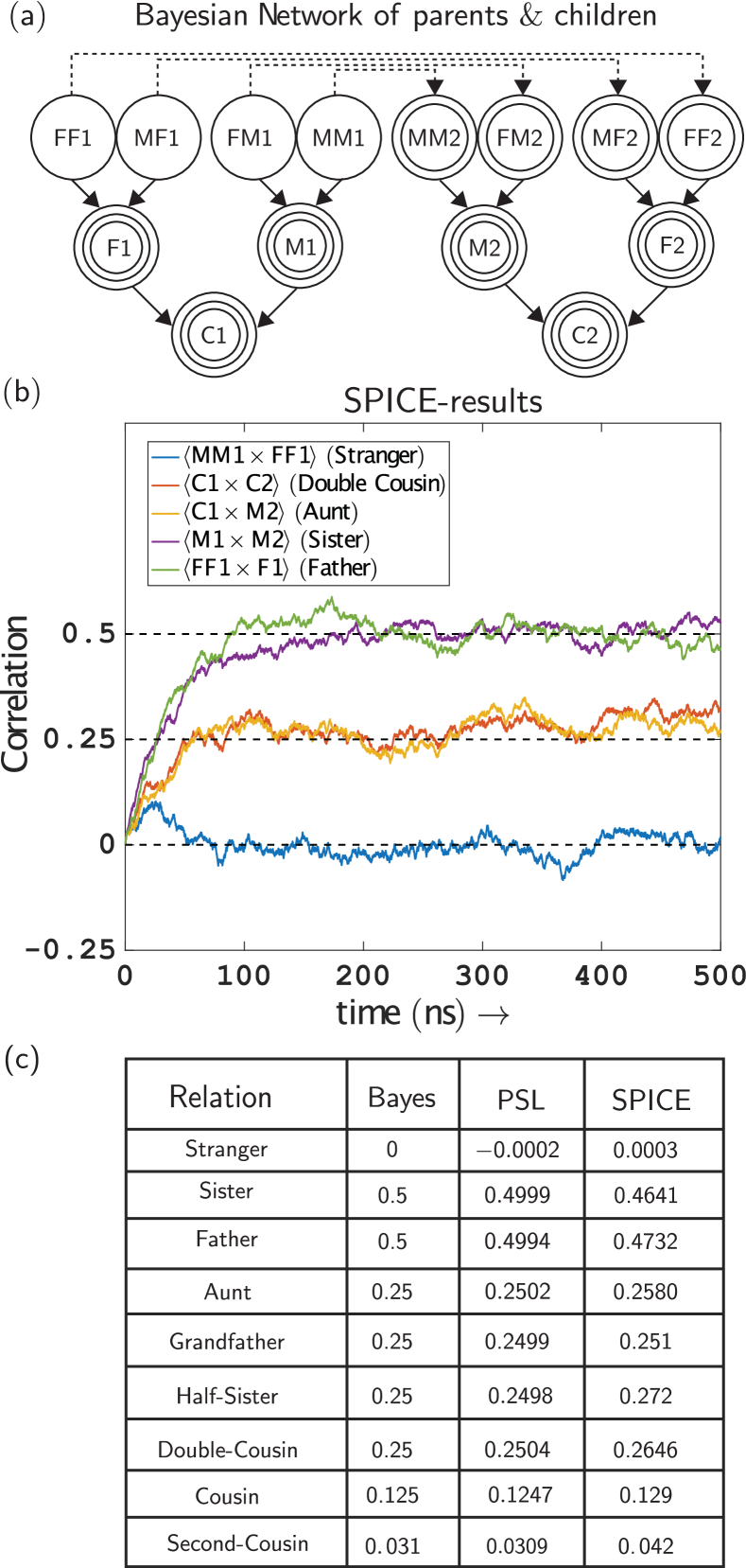
As a benchmark example, consider a BN (Fig. 1) consisting of three generations of a family, where each child () inherits half the genes from the father () and the other half from the mother (M), so that , where , and can each be viewed as a bipolar random variable: (1,1). A well-known concept in genetics is that of relatedness. For example, the relatedness of two siblings, with the same parents is On the other hand two cousins whose fathers are siblings have a relatedness of only : Fig. 1b compares the well-known relatedness of different family members (see for example, Ref. nolan_web ) with that calculated from a behavioral model which we call probabilistic spin logic, PSL, and from a simulation of the actual circuit using a SPICE-based circuit simulator.
The behavioral PSL model represents an intermediate step in the translation of BN’s to electronic circuits. It is a network whose nodes are abstract -bits denoted by (see Fig. 2) connected to other nodes and biased through dimensionless constants respectively. The -bits described by Eq. 1ba is analogous to a binary stochastic neuron and their interconnection described by Eq. 1bb is analogous to a synapse. The PSL model is then translated into a circuit model whose nodes are actual circuit elements denoted by connected to other nodes and biased through conductances and voltages . Fig. 1b shows that the relatedness from the PSL model (second column) as well as that obtained from the SPICE model (third column) agree well with the standard BN result (first column), thus providing confidence that the circuits obtained following our procedure can be used to study BN’s in general.
Genetic relatedness is a textbook concept that provides a good benchmark for a hardware circuit emulator, but the principles presented here can be used to emulate more complicated BN’s as well, involving more complex CPT’s, as well as more complex nodes with parents, reflecting the presence of more than two factors influencing the occurrence of an event.
I Probabilistic Spin Logic: Behavioral Model
PSL is defined by two equations camsari2017stochastic loosely analogous to a neuron and a synapse. The former is a binary stochastic neuron, or what we call a -bit, whose output is related to its dimensionless input by the relation
| (1a) |
where is a random number uniformly distributed between 1 and +1, and is the normalized time unit. The synapse generates the input from a weighted sum of the states of other -bits according to the relation
| (1b) |
where, is the on-site bias and is the weight of the coupling from -bit to -bit.
II From BN nodes to PSL nodes
To relate to the conditional probability for to be 1, we note from Eq. 1ba that the average value of is and this must equal =. Making use of Eq. 1bb we can write
| (2) |
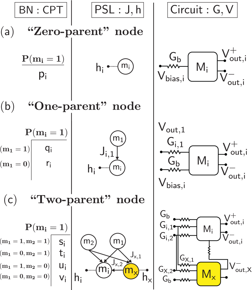
We use this relation to translate the from the CPT into in the PSL model, but the details differ depending on the number of “parents” of node (Fig. 2).
Nodes with no parents have no connecting weights , only a bias which is related to the specified conditional probability by . Nodes with one parent have one connecting weight , and a bias which can be obtained from the two specified conditional probabilities from the equations
| (3a) | |||
| (3b) |
Nodes with two parents have two connecting weights , and a bias but there are four equations for these three unknowns. All equations can be satisfied simultaneously only if the equations are not linearly independent. If they are independent then an auxiliary node is introduced so that:
| (4a) | |||
| (4b) | |||
| (4c) | |||
| (4d) |
where with the parents equal to () as appropriate for the four equations. One possibility is to choose such that and then select the four remaining unknowns to satisfy Eqs. 4d.
Nodes with parents have a total of unknowns, but there are equations to satisfy. Depending on the number of linearly independent equations, it is necessary to introduce the appropriate number of auxiliary variables. In this letter we will only present results for the BN in Fig. 1 which includes nodes with a maximum of parents. Moreover, the CPT for the 2-parent nodes is assumed to be of the form , and , being a small number introduced to avoid the singularities associated with the function. With this CPT, no auxiliary node (X) is needed.
III From PSL nodes to circuit nodes
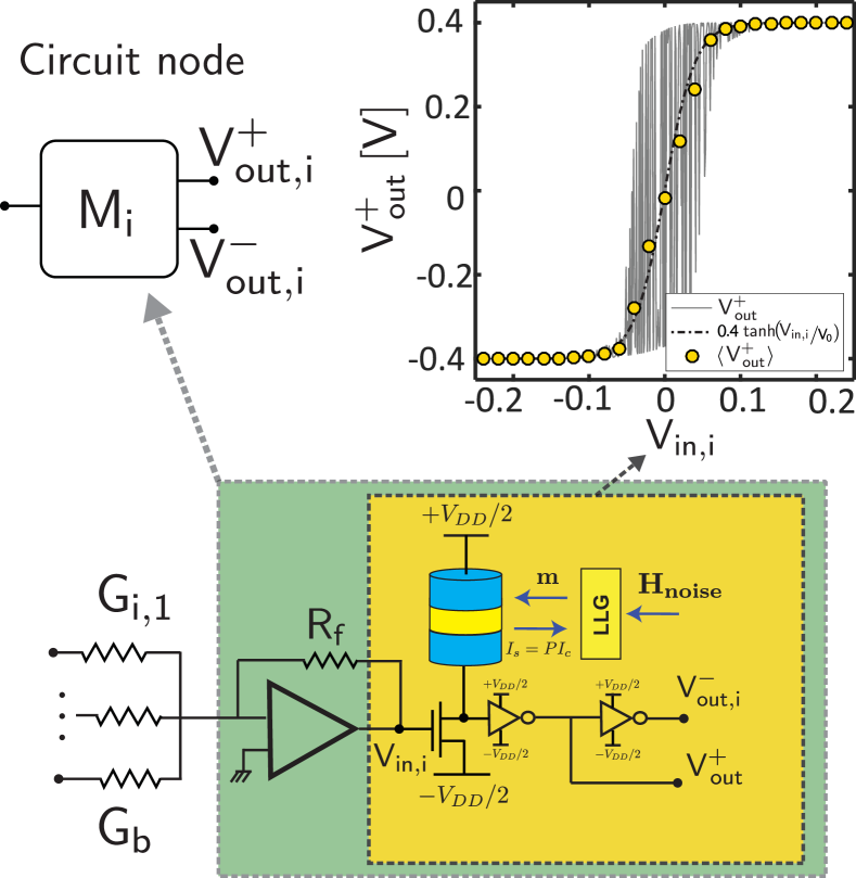
To translate the PSL into a circuit we use the embedded MTJ camsari2017stochastic whose output is related to its input by the relation
| (5a) | |||
| where are the supply voltages, and is a parameter () describing the width of the sigmoidal response. Although is a fitting parameter for the tanh function, it captures the actual sigmoidal response of the MTJ unit quite well. Even if there is a slight deviation with the tanh function due to the skewness of the MTJ response, it will not cause a noticeable difference in the output since PSL is quite robust against noise camsari2017stochastic . The output voltages are connected back through conductances with a transimpedance amplifier having a feedback resistor , so that (see Fig. 3) | |||
| (5b) | |||
Eqs. 5b can be mapped onto the PSL Eqs. 1b by defining
| (6a) | |||
| (6b) |
IV SPICE-based p-bit Model
In order to design the basic building block for the BN based on Eq. 5a, we are following the p-bit design in Ref. camsari2017implementing that describes an embedded MTJ structure with a stochastic nanomagnet. We consider the weight logic in Eq. 1bb to be implemented using ideal transimpedance amplifier with resistors camsari2017stochastic though a capacitive network with a more compact implementation could also be used to implement the weighted sum operation hassan2018voltage . We use the same parameters for the p-bit as in camsari2017implementing : A circular (stochastic) in-plane nanomagnet with negligible uniaxial anisotropy () cowburn1999single ; debashis2016experimental , damping coefficient for the nanomagnet , saturation magnetization emu/cc, with a free layer diameter 22 nm and a thickness of 2 nm. A Tunneling Magnetoresistance (TMR) value of 110% is used based on lin200945nm . The MTJ conductance is assumed to be bias-independent and is given by , where is provided to the model by a self-consistent solution of the sLLG (stochastic Landau-Lifshitz-Gilbert equation) solver. The device operation is based on the control of the transistor conductance through the input voltage. The non-linear transistor characteristics with respect to drain, gate and source voltages are captured in simulation by the 14 nm HP-FinFET node from the Predictive Technology Models (PTM) predictive_tech . When the transistor conductance is much greater or less than the MTJ conductance, the output shows little noise but when the MTJ conductance is matched to the transistor ON resistance around =0, there are large fluctuations at the output. In Fig. 3, each circular dot in the sigmoid is obtained by averaging 1 s response of the stochastic output and the dashed lines show a (tanh) fit with a mV. The solid lines are obtained by sweeping the input voltage rail-to-rail in 100 ns and plotting the input with respect to the output voltage. Within the modular SPICE framework, the magnetization dynamics of the circular stochastic nanomagnet is captured by solving the sLLG equation in the macrospin assumption,
| (7a) | |||
where is the damping coefficient, is the electron gyromagnetic ratio, Vol./ is the total number of Bohr magnetons in the magnet volume, is the saturation magnetization, is the effective field including the out-of-plane ( directed) demagnetization field , as well as the thermally fluctuating magnetic field due to the three dimensional uncorrelated thermal noise with zero mean and standard deviation along each direction, is the spin current along the MTJ fixed layer direction () where is the polarization of the fixed magnet. The model takes this spin-current () incident to the free layer into account and for the parameters we have used, this current does not cause appreciable pinning of the free layer. A time step ps is used for the circuit simulation which implies a noise bandwidth of THz.
V SPICE-based Circuit Model
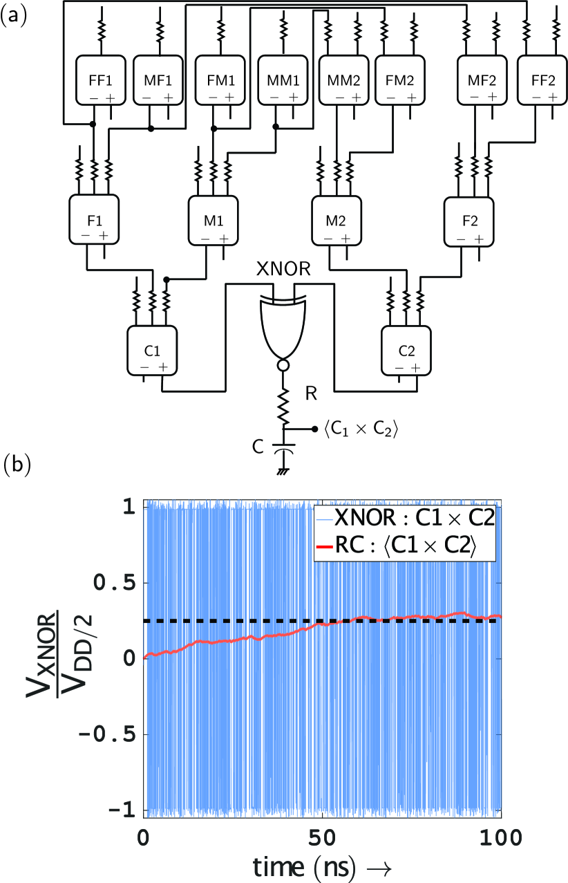
Fig. 4a shows the full circuit assembled using the nodes defined in Fig. 3 to mimic the Bayesian network in Fig. 1a. Fig. 4b shows typical nodal voltages obtained from a SPICE simulation, whose correlations can either be calculated in software or measured using an XNOR gate to multiply them as shown and finding the long term average with an RC circuit having a time constant T:
These nodal correlations in the circuit can be used to compute the correlation between causally connected real world variables. For example the relatedness of different family members cited in Fig. 1b were all obtained in this manner from circuit simulations. Different relationships between and are enforced by using different CPT’s for their grandparents. For example, if all grandparents are unrelated, the grandchildren and would show zero correlation. But if we enforce perfect correlation between , and between , through the corresponding CPT, we effectively make and into siblings with a correlation of . and then are first cousins with a correlation of .If we further enforce perfect correlation between , and between , , we also make and into siblings with a correlation of , just like and . and now are double cousins with a correlation of .
Note that this is an asynchronous circuit with no clocks of any kind. This is particularly interesting since the corresponding PSL simulations require -bits to be updated sequentially from parent to child node. In the SPICE circuit simulation there is no central clock to enforce an updating sequence, but our results show that the correlations are in good agreement with the PSL results and with Bayes theorem. However, such an asynchronous operation works only if the interconnect delays, for example from node FF1 to FF2, are much shorter than the nanomagnet fluctuations as discussed in Reference pervaiz_emulations . Since magnetic fluctuations occur at ns time scales, this condition is naturally satisfied. The slight mismatch of the Bayes theorem and the PSL model appears to decrease systematically with increasing sample size (N=1e7 for the examples shown in Fig. 1b) with the full circuit model closely following them, but the updating issue in asynchronous operation deserves further study. We have not considered variations in the thermal barriers or interconnect delays in this paper, which requires further study.
VI Conclusions
In summary, we have used SPICE simulations to show that using existing MRAM technology it should be possible to build p-circuits that mimic Bayesian networks such that each stochastic node is represented by a stochastic p-bit. We show that the ensemble-averaged correlations between the actual physical variables can be estimated from the time-averaged correlations between the voltages at the corresponding nodes which are measured electronically with XNOR logic gates and long time constant RC circuits, thus requiring no software-based processing of any kind. Our results could open up a new application space for Embedded MRAM technology with minimal modifications.
VII Acknowledgment
This work was supported by the National Science Foundation (NSF).
References
- (1) A. Fukushima, T. Seki, K. Yakushiji, H. Kubota, H. Imamura, S. Yuasa, and K. Ando, “Spin dice: A scalable truly random number generator based on spintronics,” Applied Physics Express, vol. 7, no. 8, p. 083001, 2014.
- (2) W. H. Choi, Y. Lv, J. Kim, A. Deshpande, G. Kang, J.-P. Wang, and C. H. Kim, “A magnetic tunnel junction based true random number generator with conditional perturb and real-time output probability tracking,” in Electron Devices Meeting (IEDM), 2014 IEEE International. IEEE, 2014, pp. 12–5.
- (3) H. Lee, F. Ebrahimi, P. K. Amiri, and K. L. Wang, “Design of high-throughput and low-power true random number generator utilizing perpendicularly magnetized voltage-controlled magnetic tunnel junction,” AIP Advances, vol. 7, no. 5, p. 055934, 2017. [Online]. Available:
- (4) B. Parks, M. Bapna, J. Igbokwe, H. Almasi, W. Wang, and S. A. Majetich, “Superparamagnetic perpendicular magnetic tunnel junctions for true random number generators,” AIP Advances, vol. 8, no. 5, p. 055903, 2017.
- (5) K. Y. Camsari, S. Salahuddin, and S. Datta, “Implementing p-bits with embedded mtj,” IEEE Electron Device Letters, 2017.
- (6) B. Sutton, K. Y. Camsari, B. Behin-Aein, and S. Datta, “Intrinsic optimization using stochastic nanomagnets,” Scientific Reports, vol. 7, 2017.
- (7) R. Faria, K. Y. Camsari, and S. Datta, “Low barrier nanomagnets as p-bits for spin logic,” IEEE Magnetics Letters, 2017.
- (8) A. Z. Pervaiz, L. A. Ghantasala, K. Y. Camsari, and S. Datta, “Hardware emulation of stochastic p-bits for invertible logic,” Scientific Reports, vol. 7, no. 1, p. 10994, 2017. [Online]. Available:
- (9) A. Z. Pervaiz, B. M. Sutton, L. A. Ghantasala, and K. Y. Camsari, “Weighted p-bits for fpga implementation of probabilistic circuits,” arXiv preprint arXiv:1712.04166, 2017.
- (10) K. Y. Camsari, R. Faria, B. M. Sutton, and S. Datta, “Stochastic p-bits for invertible logic,” Physical Review X, vol. 7, no. 3, p. 031014, 2017.
- (11) J. Pearl, Probabilistic reasoning in intelligent systems: networks of plausible inference. Morgan Kaufmann, 2014.
- (12) D. Heckerman, A. Mamdani, and M. P. Wellman, “Real-world applications of bayesian networks,” Communications of the ACM, vol. 38, no. 3, pp. 24–26, 1995.
- (13) D. Heckerman and J. S. Breese, “Causal independence for probability assessment and inference using bayesian networks,” IEEE Transactions on Systems, Man, and Cybernetics-Part A: Systems and Humans, vol. 26, no. 6, pp. 826–831, 1996.
- (14) I. Rish, M. Brodie, S. Ma, N. Odintsova, A. Beygelzimer, G. Grabarnik, and K. Hernandez, “Adaptive diagnosis in distributed systems,” IEEE Transactions on neural networks, vol. 16, no. 5, pp. 1088–1109, 2005.
- (15) L. N. Chakrapani, P. Korkmaz, B. E. Akgul, and K. V. Palem, “Probabilistic system-on-a-chip architectures,” ACM Transactions on Design Automation of Electronic Systems (TODAES), vol. 12, no. 3, p. 29, 2007.
- (16) S. Zermani, C. Dezan, H. Chenini, J.-P. Diguet, and R. Euler, “Fpga implementation of bayesian network inference for an embedded diagnosis,” in Prognostics and Health Management (PHM), 2015 IEEE Conference on. IEEE, 2015, pp. 1–10.
- (17) W. Tylman, T. Waszyrowski, A. Napieralski, M. Kamiński, T. Trafidło, Z. Kulesza, R. Kotas, P. Marciniak, R. Tomala, and M. Wenerski, “Real-time prediction of acute cardiovascular events using hardware-implemented bayesian networks,” Computers in biology and medicine, vol. 69, pp. 245–253, 2016.
- (18) Z. Weijia, G. W. Ling, and Y. K. Seng, “Pcmos-based hardware implementation of bayesian network,” in Electron Devices and Solid-State Circuits, 2007. EDSSC 2007. IEEE Conference on. IEEE, 2007, pp. 337–340.
- (19) Y. Shim, S. Chen, A. Sengupta, and K. Roy, “Stochastic spin-orbit torque devices as elements for bayesian inference,” Scientific Reports, vol. 7, no. 1, p. 14101, 2017.
- (20) J. S. Friedman, L. E. Calvet, P. Bessière, J. Droulez, and D. Querlioz, “Bayesian inference with muller c-elements,” IEEE Transactions on Circuits and Systems I: Regular Papers, vol. 63, no. 6, pp. 895–904, 2016.
- (21) D. Querlioz, O. Bichler, A. F. Vincent, and C. Gamrat, “Bioinspired programming of memory devices for implementing an inference engine,” Proceedings of the IEEE, vol. 103, no. 8, pp. 1398–1416, 2015.
- (22) B. Behin-Aein, V. Diep, and S. Datta, “A building block for hardware belief networks,” Scientific reports, vol. 6, 2016.
-
(23)
”(relatedness calculator)”
http://apps.nolanlawson.com/relatedness-calculator/index. - (24) O. Hassan, K. Camsari, and S. Datta, “Voltage-driven Building Block for Hardware Belief Networks,” arXiv preprint arXiv:1801.09026, 2018.
- (25) R. Cowburn, D. Koltsov, A. Adeyeye, M. Welland, and D. Tricker, “Single-domain circular nanomagnets,” Physical Review Letters, vol. 83, no. 5, p. 1042, 1999.
- (26) P. Debashis, R. Faria, K. Y. Camsari, J. Appenzeller, S. Datta, and Z. Chen, “Experimental demonstration of nanomagnet networks as hardware for ising computing,” in Electron Devices Meeting (IEDM), 2016 IEEE International. IEEE, 2016, pp. 34–3.
- (27) C. Lin, S. Kang, Y. Wang, K. Lee, X. Zhu, W. Chen, X. Li, W. Hsu, Y. Kao, M. Liu et al., “45nm low power cmos logic compatible embedded stt mram utilizing a reverse-connection 1t/1mtj cell,” in Electron Devices Meeting (IEDM), 2009 IEEE International. IEEE, 2009, pp. 1–4.
- (28) Predictive Technology Model (PTM) (http://ptm.asu.edu/).