Present address: ]NTT Basic Research Laboratories, NTT Corporation, 3-1 Morinosato Wakamiya, Atsugi, Kanagawa 243-0198, Japan
LO-phonon emission rate of hot electrons from an on-demand single-electron source in a GaAs/AlGaAs heterostructure
Abstract
Using a recently-developed time-of-flight measurement technique with 1 ps time resolution and electron-energy spectroscopy, we developed a method to measure the longitudinal-optical-phonon emission rate of hot electrons travelling along a depleted edge of a quantum Hall bar. A comparison of the experimental results to a single-particle model implies that the main scattering mechanism involves a two-step process via intra-Landau-level transition. We show this scattering can be suppressed by controlling the edge potential profile, and a scattering length 1 mm can be achieved, allowing the use of this system for scalable single-electron device applications.
The development of accurate, on-demand, hot single electron sources has opened up a new energy domain in which to study fundamental electron behaviour in the solid state Blumenthal et al. (2007); Kaestner et al. (2008); Leicht et al. (2011); Giblin et al. (2012). In particular, this energy domain presents a unique environment in which we can study the nature of single-particle physics. One extensively studied phenomenon of hot electrons in GaAs systems is the energy relaxation by emission of longitudinal optical (LO) mode phonons Heiblum et al. (1985); Das Sarma and Madhukar (1980); Das Sarma and Campos (1994); Sivan et al. (1989); Taubert et al. (2011, 2010). This causes the electrons to undergo a discrete energy loss ( 36 meV) per emission of one LO phonon. This inelastic scattering process is one of the reasons that high-energy quasiparticles are considered to be inappropriate for experiments that require electron coherence, such as interferometry. Suppression of this scattering mechanism creates a possibility to utilise these devices for experiments such as electron quantum optics Bocquillon et al. (2013) and technological applications Bennett and DiVincenzo (2000). Therefore, it is important to characterise the rate of LO-phonon scattering and understand its mechanisms. However, it has so far not been straightforward to measure the rate directly in transport measurements, because although it is relatively easy to measure the scattering probability, it is not easy to measure the electron velocity. Moreover, in the presence of a background Fermi sea, electron-electron interactions strongly affect the system, masking the simple single-particle physics Taubert et al. (2010). Now with the development of on-demand hot single-electron sources Blumenthal et al. (2007) and electron energy spectroscopy Fletcher et al. (2013), it is possible to perform energy- and time-resolved study of hot electron transport through an intrinsic/depleted region free from electron-electron interactions.
In this work we present measurements of the LO-phonon emission rate of hot electrons travelling in quantum Hall edge states. In order to deduce the LO phonon emission rate, we first measure the LO phonon emission probability along an electron path with length using energy spectroscopy Fletcher et al. (2013). Then, we measure the average electron drift velocity (or electron travel time ) in the same path using a time-of-flight measurement Kataoka et al. (2016a). The scattering rate is calculated as . We perform a detailed study of how the emission rate varies as electron energy, edge-potential profile and magnetic field are varied. Comparison with theory for direct LO-phonon emission Emary et al. (2016) shows that, while qualitatively in agreement, our measured rate is many orders of magnitude larger than the predicted values. We suggest that an enhanced emission process due to an inter-Landau-level transition may be present Komiyama et al. (1992). Moreover, we demonstrate that the scattering length can be made as large as 1 mm by controlling the edge potential.
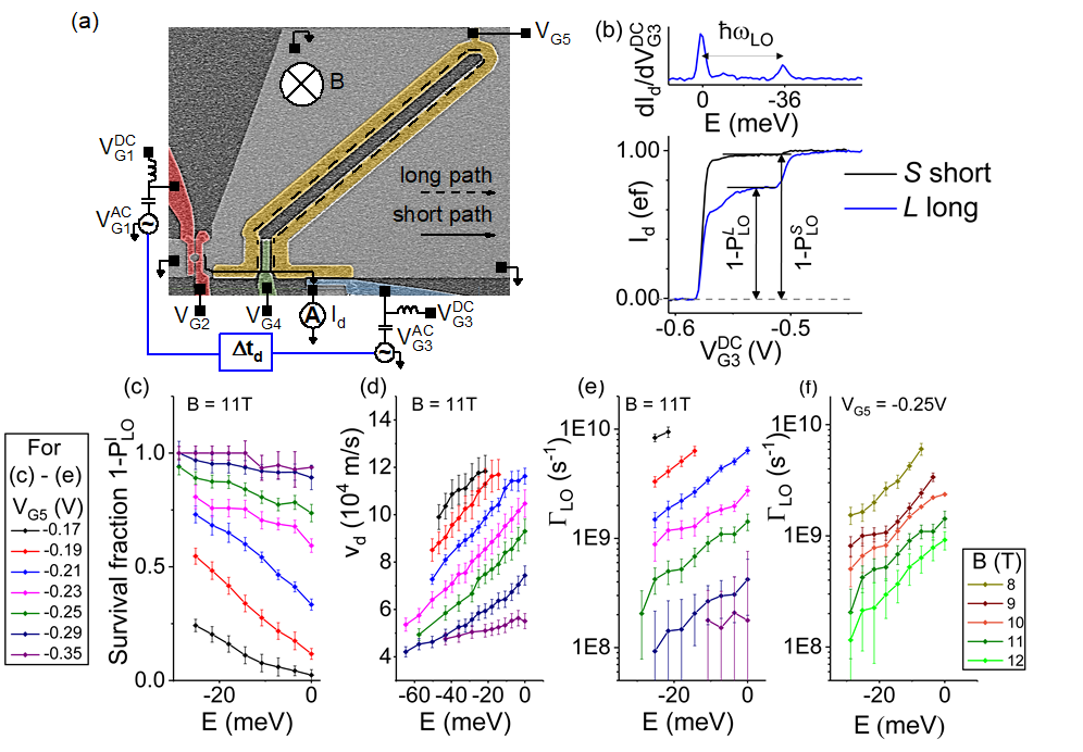
A scanning-electron-microscope (SEM) image of an identical device to that used, with schematic electrical connections, is shown in Fig. 1(a). The sample has a similar geometry to those used in Ref. Kataoka et al. (2016a). A two-dimensional electron gas (2DEG) is defined 90 nm below the surface of a GaAs/AlGaAs heterostructure. Parts of the substrate are chemically etched using electron-beam lithography to define the mesa shown in light grey in Fig. 1(a) (including the area encircled by the yellow gate). Five Au/Ti metallic gates are patterned onto the surface using electron-beam lithography. Gates G1 and G2, shaded in red, define the quantum dot single-electron pump that acts as the source of energy-tunable hot electrons Blumenthal et al. (2007); Kaestner et al. (2008); Leicht et al. (2011); Giblin et al. (2012). G1 is driven by an ac sinusoidal waveform at frequency MHz with a peak-to-peak amplitude 1 V from one channel of an arbitrary waveform generator (AWG), in addition to a dc voltage . We tune the gate voltages to pump one electron per cycle, producing a current pA, with the elementary charge.
In the presence of a perpendicular magnetic field , the electrons emitted from the pump travel along the sample edge either in the short (5 m) or long path (28 m) indicated by the solid and dashed lines respectively in Fig. 1(a), just as in the edge-state transport in the quantum Hall regime Halperin (1982), but with an energy (about 100 meV) above the Fermi energy Fletcher et al. (2013). The voltage applied to the deflection gate determines which path the electrons take 111This is the lithographic length, and we assume a error because we do not know the exact path the electrons take. We note that the error in path length estimate does not contribute to the error in the measurements of phonon emission rate as it is cancelled out by both the velocity and length estimates. It does, however, contribute to the error in the estimate of the edge potential profile.. The time-of-flight method in Ref. Kataoka et al. (2016a) gives the electron velocity in the loop section (the part that encircles the elongated etched area and does not include the paths along the gate ) of length m (see supplemental material for determination of this length). This is the length where we investigate the LO-phonon emission rate.
Gate (blue) is the detector gate. A dc gate voltage is used to detect the electron energy Fletcher et al. (2013) and the LO phonon emission probability by measuring the transmitted detector current . For the time-of-flight measurements, an ac square waveform , with controllable time delay , is applied in addition to Kataoka et al. (2016a); Waldie et al. (2015); Johnson et al. (2017); Kataoka et al. (2016b). Gate G5 (yellow) is the depletion gate, and is used to change the potential profile at the edge where electrons propagate by applying a dc voltage . We note that, throughout this work, the voltage applied to the depletion gate is negative enough to deplete the 2DEG underneath, but not negative enough to push the path of our hot electrons outside the gated region. Experiments are performed in a dilution refrigerator with a base temperature 30 mK and with a perpendicular magnetic field of 8 - 12 T.
In order to determine the LO-phonon emission rate, we first measure the probability of emission in the long (short) path . This is done by measuring while sweeping the detector . This gives us a certain fraction of pumped current , which is the proportion of pumped electrons that retain enough energy to pass the detector barrier. Fig. 1(b) shows an example of this measurement taken for the short (black) and long (blue) paths 222In this example, V, V, T, and V (short path, ) or V (long path, ).. As is swept to a more positive value (i.e. as the detector barrier is lowered), increases and shows a sub-step (the phonon plateau) before rising to and saturating. The derivative shows two peaks as shown in the top panel in Fig. 1(b). From Ref Fletcher et al. (2013), we identify the left-hand peak as the energy spectrum of electrons at the original emission energy, and the right-hand peak as that of electrons that have emitted one LO phonon before arriving at the detector. From this, we can convert the scale into the energy scale, assuming meV. The height of the phonon plateau (when normalised to ) gives a survival fraction of electrons arriving at the detector without any LO-phonon emission, i.e. for long (short) path.
We then deduce the survival fraction in the loop alone by noting that the long path survival fraction is the product of the survival fractions of the short path and the loop, i.e. . With our single-electron source, the electron emission energy can be tuned by changing the height of the exit barrier, i.e. by varying Fletcher et al. (2013). Fig. 1(c) shows as a function of the electron emission energy (here, we define for the highest emission energy used) taken with a different value of depletion gate voltage , at T. We also measure the average electron drift velocity (of the non-LO-phonon emitting fraction) in the loop section for different electron emission energy using the method described in Ref. Kataoka et al. (2016a) [Fig. 1(d)]. (We will later calculate the form of the edge potential profile from these data.) Assuming the constant rate of LO phonon emission throughout the loop, we can calculate the rate as [Fig. 1(e)] 333We note that there is a smaller number of data points in Fig. 1(e) compared to Fig. 1(c) and (d). This is because we need both and available in order to deduce for a given experimental condition. The range in for which can be measured is limited because, as the original electron emission is lowered below meV (the energy of the electron that emits one phonon will be below -61 meV), we cannot reliably measure the height of the sub-step in as a spurious current due to a pick up of RF signal by the 2DEG starts to flow through the detector barrier when it is made too low. Also, measurement is difficult for less negative and higher , where the LO phonon emission rate is high, as there are not enough electrons reaching the detector with the original emission energy, so cannot be detected by the measurement of .. We observe that the rate of phonon emission is strongly a function of both emission energy and . In Fig. 1(f) we repeat this analysis at various values, for the case . We also clearly see a strong field dependence on the rate of phonon emission, with emission suppressed at higher fields Fletcher et al. (2013). We note that the reason that there is no data below in Fig. 1(e) is not because we cannot tune the device into that regime, but because the scattering probability becomes so small that it is difficult to detect it by the measurement of the detector current. If we extrapolate the data for V to meV [experimental data for survival probability in this configuration is shown in Fig. 1(c)], and m/s. Hence, we expect the scattering length to be mm in this configuration. The scattering length can easily be made even longer.
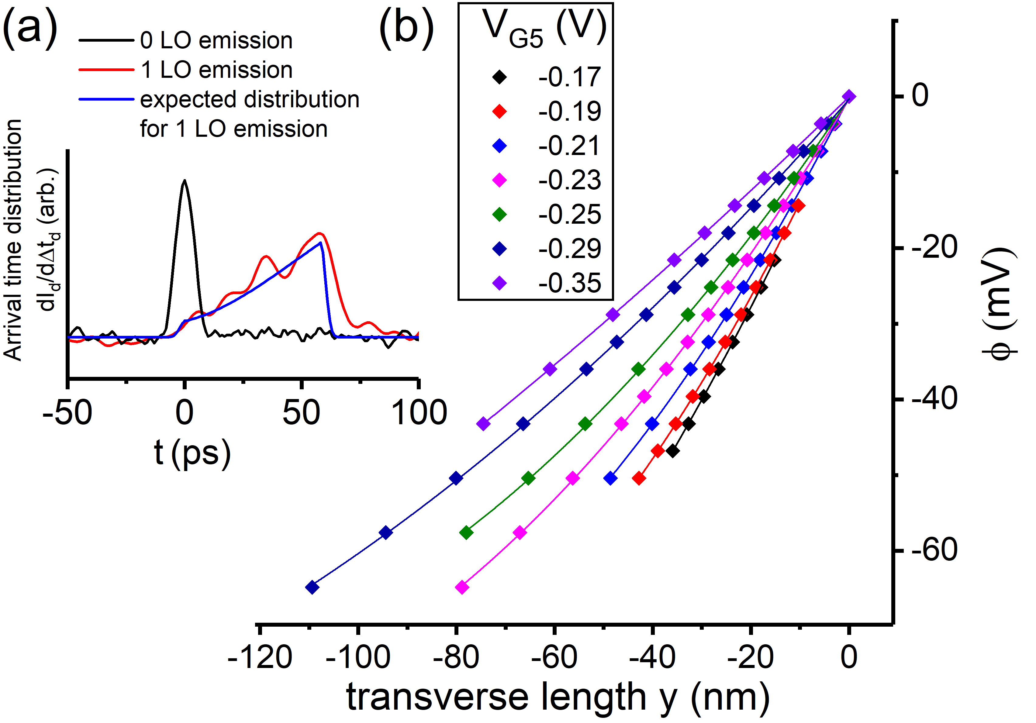
Because we have temporal detection of the electrons, we can detect whether the phonon emission happens uniformly around the ring, or whether there are phonon emission ‘hot spots’. If the latter is the case, the measured phonon emission rate by our technique may not represent the actual emission rate. A phonon-emission hot spot will produce a peak in the arrival-time distribution, of the electrons that have emitted one LO phonon. This peak in is expected to occur later than the peak of the original electrons, as the electrons at a lower energy are expected to travel at a lower velocity. However, if the phonon emission rate is constant throughout the path, we expect the arrival-time distribution to spread out, as electrons emit phonons at various parts of the path. In Fig. 2(a), the measurement of arrival time distribution, using the method given in Refs. Waldie et al. (2015); Kataoka et al. (2016b), is shown for the electrons with original emission energy (black) and the electrons that have emitted one phonon (red). The expected form of (blue) with constant emission rate as calculated from Ref. Emary et al. (2016) (and see supplemental material), and shows a good match with the experimental data. This implies that our assumption of constant phonon emission rate is reasonable.
Now we investigate if our experimental results can be explained within the framework of an existing single-phonon emission model Das Sarma and Madhukar (1980); Das Sarma and Campos (1994); Emary et al. (2016). To compare the measured rate against theory, we need to know the shape of the potential profile , from which we can calculate the electronic wave function. A key parameter in the calculation of emission rates is the edge potential profile, as this dictates the spatial position of the electron before and after emission. This can be deduced from the drift velocity measurements using the method described in Ref. Kataoka et al. (2016a), and we plot the deduced potential profile in Fig. 2(b), for each case of we have measured the LO-phonon rate, under the same conditions as the emission rate was measured.
The theoretical LO-phonon emission rate can be calculated using the method described in Ref. Emary et al. (2016), by performing the harmonic fit to the experimentally determined potential profiles, . [We note that we use a z-confinement (in the substrate growth direction) of 10 nm, the variation of which within 50% does not change the order of magnitude of the result, and is the only free parameter in the model.] Fig. 3(a) plots the experimental data [square symbols, same as that presented in Fig. 1(e)] and calculated LO phonon emission rate (solid lines) for intra-Landau-level transition (, where is the Landau level index) [red arrow in Fig. 3(b)] for different values of . In Fig. 3(c), the ratio of the theoretically calculated value and experimental value is plotted, showing a large discrepancy by many orders of magnitude. When only direct LO-phonon emission is considered, the predicted rates of emission are far lower than those measured experimentally. In order to explain this discrepancy, we consider the possibility that there are other paths to phonon emission.
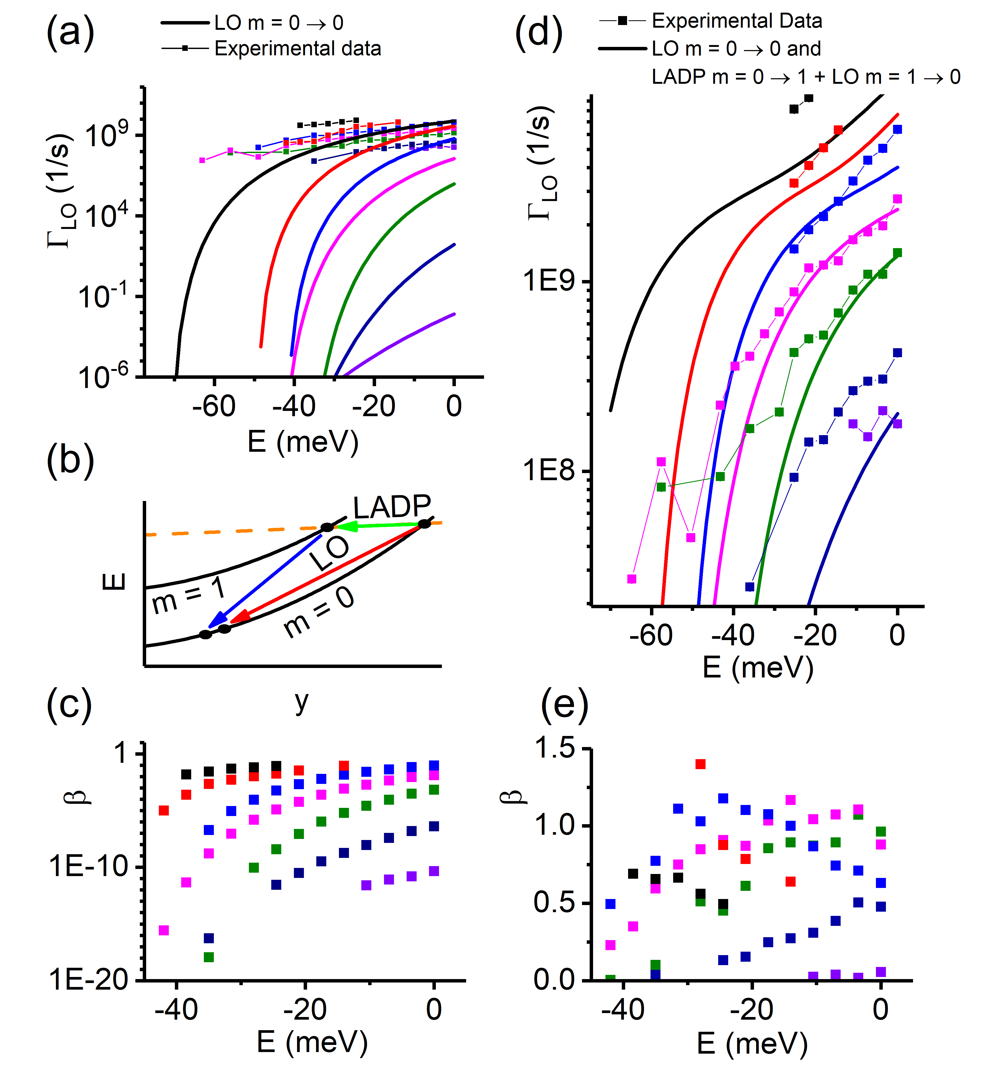
One such possibility is a process in which an electron is first transferred to the Landau level via longitudinal acoustic via deformation potential (LADP) mode Climente et al. (2006); Komiyama et al. (1992) and then is transferred back to the Landau level via LO-phonon emission [see the green and blue arrows in Fig. 3(b)]. This two-step process can be faster than the direct transition. This is because the rate of any particular transition is proportional to the electronic wave function overlap and thus to a factor , where is the change in the guide-centre coordinate in the transition and is the magnetic length Emary et al. (2016). Since can be smaller in each of the emissions in the two-stage process, an exponential speed-up is gained and in some circumstances, this can overcome the inherent slowness of a two step process. The sum of the direct and two-step rates are shown in Fig. 3(d), and the ratio is plotted in Fig. 3(e). This clearly shows that the calculated curves agree with experiments within an order of magnitude, except for those with the most negative values of . Here, the edge-confinement potential is shallower, and harmonic approximation may be inadequate, which may be the origin of the discrepancy.
In summary, we have demonstrated a detailed study of LO-phonon emission rate of hot electrons in quantum Hall edge states. We measured this rate at different electron energies, magnetic fields, and under different potential profiles, which is controlled by an edge depletion gate that covers the whole electron path from pump to detector. The depletion of the background electron gas allows us to study these effects within a simple single-particle picture. Comparisons with theory suggest that inter-Landau-level scattering via acoustic phonon emission is involved in the LO-phonon emission. We found that the phonon emission rate can be controlled by the edge-depletion gate, and scattering length can be enhanced as much as 1 mm or even longer, which enables the construction of large-scale single-electron devices.
We thank S. P. Giblin and S. Ludwig for useful discussions. This research was supported by the UK Department for Business, Energy, and Industrial Strategy, the UK EPSRC, and by the project EMPIR 15SIB08 e-SI-Amp. This project has received funding from the EMPIR programme co-financed by the Participating States and from the European Union’s Horizon 2020 research and innovation programme and by Korea NRF (Grant No. 2016R1A5A1008184).
References
- Blumenthal et al. (2007) M. D. Blumenthal, B. Kaestner, L. Li, S. Giblin, T. J. B. M. Janssen, M. Pepper, D. Anderson, G. Jones, and D. A. Ritchie, Nature Phys. 3 343 (2007).
- Kaestner et al. (2008) B. Kaestner, V. Kashcheyevs, G. Hein, K. Pierz, U. Siegner, and H. W. Schumacher, App. Phys. Lett. 92 192106 (2008).
- Leicht et al. (2011) C. Leicht, P. Mirovsky, B. Kaestner, F. Hohls, V. Kashcheyevs, E. V. Kurganova, U. Zeitler, T. Weimann, K. Pierz, and H. W. Schumacher, Semicond. Sci. Tech. 26 055010 (2011).
- Giblin et al. (2012) S. P. Giblin, M. Kataoka, J. D. Fletcher, P. See, T. J. B. M. Janssen, J. P. Griffiths, G. A. C. Jones, I. Farrer, and D. A. Ritchie, Nature Comms. 3 1935 (2012).
- Heiblum et al. (1985) M. Heiblum, M. I. Nathan, D. C. Thomas, and C. M. Knoedler, Phys. Rev. Lett. 55 2200 (1985).
- Das Sarma and Madhukar (1980) S. Das Sarma and A. Madhukar, Phys. Rev. B 22 2823 (1980).
- Das Sarma and Campos (1994) S. Das Sarma and V. B. Campos, Phys. Rev. B 49, 1867 (1994).
- Sivan et al. (1989) U. Sivan, M. Heiblum, and C. P. Umbach, Phys. Rev. Lett. 63 9 (1989).
- Taubert et al. (2011) D. Taubert, C. Tomaras, G. J. Schinner, H. P. Tranitz, W. Wegscheider, S. Kehrein, and S. Ludwig, Phys. Rev. B 83, 235404 (2011).
- Taubert et al. (2010) D. Taubert, G. J. Schinner, H. P. Tranitz, W. Wegscheider, C. Tomaras, S. Kehrein, and S. Ludwig, Phys. Rev. B 82 161416R (2010).
- Bocquillon et al. (2013) E. Bocquillon, V. Freulon, J. M. Berroir, P. Degiovanni, B. Plaçais, A. Cavanna, Y. Jin, and G. Fève, Science 339 (6123) 1054 (2013).
- Bennett and DiVincenzo (2000) C. H. Bennett and D. P. DiVincenzo, Nature 404 247 (2000).
- Fletcher et al. (2013) J. D. Fletcher, P. See, H. Howe, M. Pepper, S. P. Giblin, J. P. Griffiths, G. A. C. Jones, I. Farrer, D. A. Ritchie, T. J. B. M. Janssen, and M. Kataoka, Phys. Rev. Lett. 111 216807 (2013).
- Kataoka et al. (2016a) M. Kataoka, N. Johnson, C. Emary, P. See, J. P. Griffiths, G. A. C. Jones, I. Farrer, D. A. Ritchie, M. Pepper, and T. J. B. M. Janssen, Phys. Rev. Lett. 116, 126803 (2016a).
- Emary et al. (2016) C. Emary, A. Dyson, S. Ryu, H.-S. Sim, and M. Kataoka, Phys. Rev. B 93, 035436 (2016).
- Komiyama et al. (1992) S. Komiyama, H. Hirai, M. Ohsawa, Y. Matsuda, S. Sasa, and T. Fujii, Phys. Rev. B 45 11085 (1992).
- Halperin (1982) B. I. Halperin, Phys. Rev. B 25 2185 (1982).
- Note (1) This is the lithographic length, and we assume a error because we do not know the exact path the electrons take. We note that the error in path length estimate does not contribute to the error in the measurements of phonon emission rate as it is cancelled out by both the velocity and length estimates. It does, however, contribute to the error in the estimate of the edge potential profile.
- Waldie et al. (2015) J. Waldie, P. See, V. Kashcheyevs, J. P. Griffiths, I. Farrer, G. A. C. Jones, D. A. Ritchie, T. J. B. M. Janssen, and M. Kataoka, Phys. Rev. B 92, 125305 (2015).
- Johnson et al. (2017) N. Johnson, J. D. Fletcher, D. Humphreys, P. See, J. Griffiths, G. Jones, I. Farrer, D. Ritchie, M. Pepper, T. Janssen, and M. Kataoka, Appl. Phys. Lett. 110 102105 (2017).
- Kataoka et al. (2016b) M. Kataoka, J. D. Fletcher, and N. Johnson, Phys. Status Solidii B 254 1521 (2016b), 10.1002/pssb.201600547.
- Note (2) In this example, V, V, T, and V (short path, ) or V (long path, ).
- Note (3) We note that there is a smaller number of data points in Fig. 1(e) compared to Fig. 1(c) and (d). This is because we need both and available in order to deduce for a given experimental condition. The range in for which can be measured is limited because, as the original electron emission is lowered below meV (the energy of the electron that emits one phonon will be below -61 meV), we cannot reliably measure the height of the sub-step in as a spurious current due to a pick up of RF signal by the 2DEG starts to flow through the detector barrier when it is made too low. Also, measurement is difficult for less negative and higher , where the LO phonon emission rate is high, as there are not enough electrons reaching the detector with the original emission energy, so cannot be detected by the measurement of .
- Climente et al. (2006) J. I. Climente, A. Bertoni, G. Goldoni, and E. Molinari, Phys. Rev. B 74 035313 (2006).