Irradiation study of a fully monolithic HV-CMOS pixel sensor design in AMS 180 nm
Abstract
High-Voltage Monolithic Active Pixel Sensors (HV-MAPS) based on a 180 nm HV-CMOS process have been proposed to realize thin, fast and highly integrated pixel sensors. The MuPix7 prototype, fabricated in the commercial AMS H18 process, features a fully integrated on-chip readout, i.e. hit-digitization, zero suppression and data serialization. MuPix7 is the first fully monolithic HV-CMOS pixel sensor that has been tested for the use in high irradiation environments like HL-LHC. We present results from laboratory and test beam measurements of MuPix7 prototypes irradiated with neutrons (up to ) and 24 GeV protons (up to ) and compare the performance with non-irradiated sensors. At sensor temperatures of about efficiencies of at noise rates below 40 Hz per pixel are measured for fluences of up to . A time resolution better than , expressed as Gaussian , is measured for all tested settings and sensors, even at the highest irradiation fluences. The data transmission at 1.25 Gbit/s and the on-chip PLL remain fully functional.
keywords:
HV-CMOS , monolithic active pixel sensors , radiation-hard detectors , particle tracking detectors1 Introduction
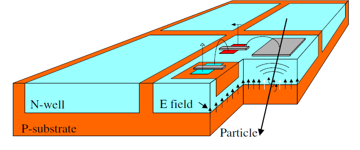
High-Voltage Monolithic Active Pixel Sensors (HV-MAPS) have been proposed [1] as an alternative to hybrid detectors. High-Voltage CMOS processes allow for the implementation of strong electric drift fields in a thin active depletion region as small as . The main mechanism for charge collection is therefore drift in contrast to standard MAPS where the charge is mainly collected by diffusion. Due to the small depletion region for the standard low resistivity substrates () and biasing from the top side, the inactive p-substrate can be removed allowing for thin sensors. The small depletion region makes HV-CMOS designs also less sensitive to charge trapping caused by radiation damage of the bulk, which reduces the effective charge collection distance.
The AMS H18 process [2] is a commercial HV-CMOS process providing high reliability at moderate production cost. It allows for the integration of analogue readout electronics into an active pixel matrix as well as the implementation of digital electronics as seen in figure 1. In this paper the performance of a fully monolithic222I.e. signal amplification, digitization, zero supression, time stamp sampling, readout state-machine and data serialization is implemented on chip. HV-MAPS prototype after proton and neutron irradiation is studied for the first time.
For another sensor with a similar pixel cell design and hybrid readout (CCPDv4 [3]), it was shown that the analogue pixel performance remains high after particle fluences of up to [4]. Additional studies with prototypes of Depleted Monolithic Active Pixel Sensor (DMAPS) based on a modified CMOS process from TowerJazz [5] have also shown high efficiencies after irradition with up to .
The MuPix HV-MAPS prototypes studied here have been developed for the Mu3e experiment [6] using the IBM/AMS H18 process. To test the radiation tolerance, ten MuPix7 prototype sensors were irradiated without bias at room temperature with 24 GeV protons at the CERN PS [7] and with neutrons at the TRIGA reactor at the Jožef Stefan Institute [8] in Ljubljana, with particle fluences up to and , respectively.
2 MuPix7 prototype
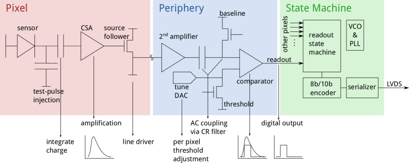
The fully monolithic MuPix7 prototype [9] is the first HV-MAPS integrating all functionalities required for a data driven readout, realized on a substrate. It consists of a pixel matrix with a pixel size of , resulting in an active size of and a total size of . Each pixel cell integrates a charge sensitive amplifier with a source follower driving the signal to the periphery, see figure 2. In the periphery, the analogue signal is amplified in a second stage and discriminated against a threshold which can be fine-adjusted for each pixel. The pixel address and an time stamp generated at are stored and read out by an on-chip state machine. The zero suppressed data are / encoded, serialized and transmitted at a rate of over a SCSI II cable with a length of . The MuPix7 prototype does not contain additional measures like ring transistors or triple redundant logic to increase the radiation tolerance of the sensor. The MuPix7 has a set of configuration DACs to adjust the response of the amplifier, the line driver strength, the state machine frequency, etc. These global MuPix configuration settings have been optimized once for the non irradiated sensors, corresponding to a power consumption of and are used without changes for all irradiated MuPix prototypes.
Previous studies have shown that non-irradiated MuPix7 sensors have an efficiency of above at per-pixel noise rates below and a depletion voltage of [9, 10, 11]. The time resolution was measured to be below . When using an Fe-55 source approximately 1600 primary electrons are expected for an non-irradiated MuPix7 with an average signal of [12].
Four dedicated columns of the MuPix7 matrix implement single stage amplification and are not considered in the presented measurements.
Irradiated samples
MuPix7 sensors have been irradiated with protons and neutrons according to table 1. During irradiation, the sensors have not been biased and not cooled. The prototypes had not been characterized beforehand. The samples have sensor thicknesses of and . The studies have been performed after one year of annealing at room temperature and therefore complete annealing of the ionizing damage is expected. The non-ionizing damage responsible for charge trapping and bulk damage, however, is expected to be left unchanged and is the primary focus of this study.
| Sensor ID | P00 | P814 | P1515 | P7815 | N00 | N514 | N115 | N515 |
|---|---|---|---|---|---|---|---|---|
| Facility | - | PS | PS | PS | - | TRIGA | TRIGA | TRIGA |
| NIEL Fluence [1 MeV ] | 0 | 0 | ||||||
| Proton Fluence [24 GeV/c ] | 0 | - | - | - | - |
3 Setup
The proton irradiated sensors are directly glued and wire-bonded to a printed-circuit-board (PCB). The neutron irradiated sensors are glued and wire-bonded to a ceramic carrier, which is connected to the same PCB type via a socket333Due to limited availability of PCBs only the proton irradiated sensors were directly bonded to PCBs.. The PCB provides stable and ripple-free power, filters the high voltage and converts the differential slow control signals to single ended signals required by the MuPix7. Baseline and threshold reference for the sensor are generated on the PCB where also test pulses to mimic signals can be generated.
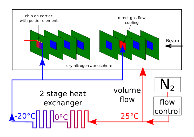
The test beam setup is sketched in figure 3. The sensors under test are actively cooled to reduce leakage currents and noise while also preventing thermal runaway. The proton irradiated sensors are cooled by cold nitrogen gas flowing over the backside of the sensor. The neutron irradiated sensors are cooled using a Peltier element, connected with an aluminum chuck. The Peltier element in turn is cooled by cold nitrogen gas. Two thermal baths are used to cool the nitrogen gas to for both setups. The cooling power of the setup is controlled by the applied gas flow. A combined nitrogen flow of is used to cool the two sensors under test. The temperature of both devices-under-test (DUTs), as well as the humidity in the box, are continuously monitored to guarantee safe and constant operation conditions. Two reference tracking telescopes [14], consisting of three non-irradiated, uncooled MuPix7 sensors each, are used to measure efficiencies.
Temperature calibration
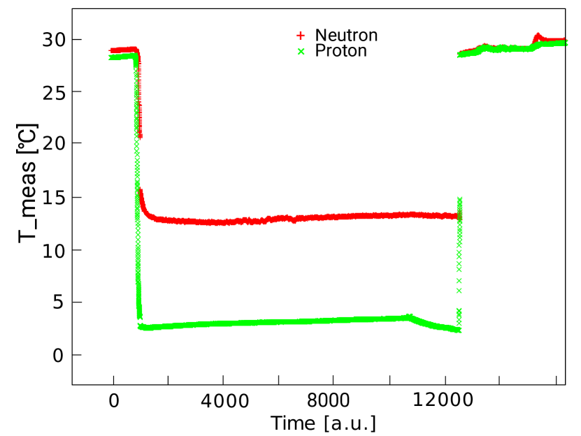
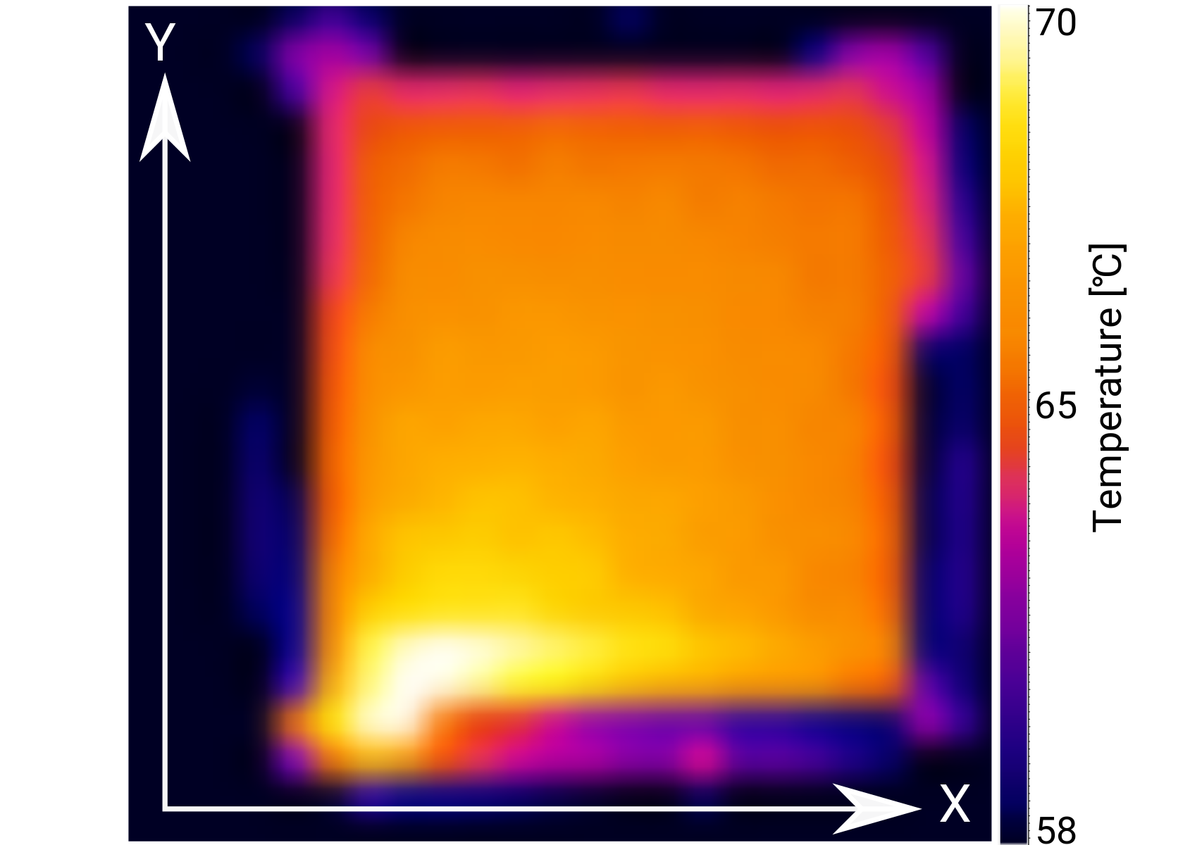
The temperature of the proton irradiated MuPix is monitored by measuring the gas temperature close to the MuPix. The temperature of the neutron irradiated prototypes is monitored by measuring the cooling chuck temperature. For both devices the MuPix temperature is calculated from the measured temperatures by applying a correction obtained from an IR-camera444The IR-camera in turn had been calibrated using a Pt1000 [15] glued on a heatable reference silicon surface.. The correction is about for the proton (neutron) irradiated prototypes. The uncertainty on the absolute temperature is dominated by the reproducibility of the thermal coupling between MuPix and temperature sensor and estimated to be . The relative uncertainty of the measured temperature over time is small and mainly given by the temperature sensor’s uncertainty of . The temperature is stable on the level for measurement periods of , see figure 4. The MuPix temperature for both, proton and neutron irradiated, sensors is approximately .
4 Characterization of irradiated sensors
4.1 Laboratory results
All irradiated MuPix7 are fully operational after irradiation: the PLL can be locked to an external 125 MHz reference oscillator and the serial data output runs without / errors. All hit addresses and time stamps transmitted to the FPGA are checked to be logically correct, thus indicating a fully functional readout state machine and serializer.
Leakage currents
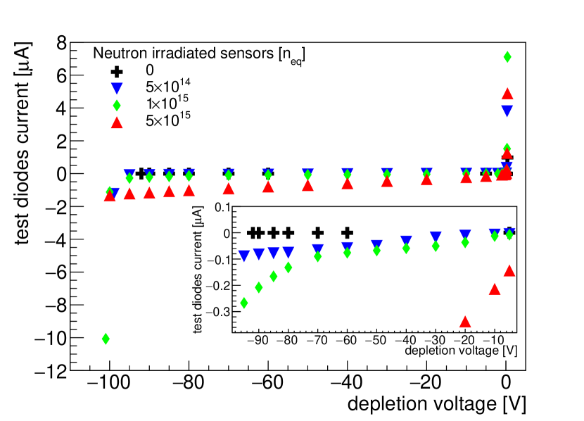
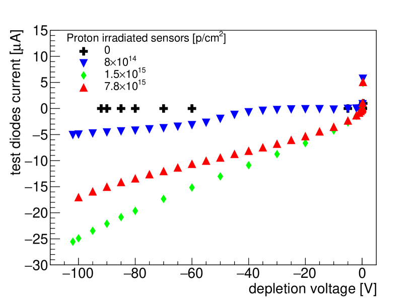
The leakage currents of non-irradiated and irradiated sensors are measured as a function of the depletion voltage. Figures 5(a) and 5(b) show the current-voltage characteristic (IV curve) for the neutron- and proton-irradiated sensors at room temperature when only depletion voltage is applied to a set of dedicated test diodes. As expected the measured leakage current significantly increases with the particle fluence and applied voltage. However, the absolute leakage current increase for the proton irradiated sensors is about twenty times higher than for the neutron irradiated sensors for similar fluences. A possible explanation is that the hardness factor for protons is significantly larger than expected for low-ohmic silicon wafers and the AMS-H18 process555Similar effects, indicating an enhanced acceptor removal in low ohmic substrates, have been reported by other groups and are under investigation.. It is also a bit surprising that the sample shows less leakage currents than the sample. From edge-TCT measurements [16] it is known that the depletion thickness has a maximum for a fluence of about which possibly could explain the higher leakage currents.
The diode breakdown voltage is below for all irradiated samples666The exact value of the breakdown voltage was not measured to minimize the risk of damage. and is significantly lower than the non-irradiated sensors, which have a typical breakdown voltage of about . This is consistent with an increased depletion thickness after irradiation [16].
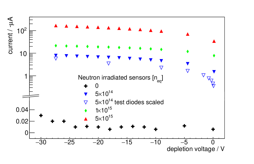
The leakage currents of all irradiated sensors in full operation are shown in figure 6 as a function of the depletion voltage. The slightly larger current compared to the measurements of the test diodes in figure 5(a) can be explained by the higher temperature of the sensor in full operation, see figure 7. Without active cooling it is not possible to operate the sensors with depletion voltages below due to thermal runaway. With cooling, for T , the MuPix can be operated up to a depletion voltage of . The following measurements are obtained with the active cooling system described in section 3 at a MuPix temperature of about .
Pixel tuning
In MuPix7, pixel-to-pixel variations can be corrected for with a tuning DAC (TDAC), by adjusting the discriminator threshold. A global DAC (VPDAC) selects from the externally provided threshold reference the tuning range covered by the TDACs. Higher TDAC values correspond to higher effective thresholds, i.e. the separation between threshold and baseline is increased. The pixel response adjustment is based on a noise measurement and an automated software calibration scheme is used. The threshold reference and the VPDAC value are selected such that all pixels are below a certain noise rate at the maximal TDAC value. Afterwards, each individual TDAC value is adjusted such that the noise rate of every pixel is just below the target noise rate ( without beam). The thresholds obtained by the automated tuning routine strongly vary between sensors and depend on the applied depletion voltage and the irradiation fluence. A summary of the tested sensors, the corresponding tune thresholds and VPDAC values is given in table 2. For the proton irradiated samples, the described tuning procedure does not work properly for the complete matrix because of too large pixel-to-pixel variations caused by the inhomogeneities in the irradiation process (see below). Therefore, up to 5% of all pixels777Pixels cannot be masked in the MuPix7. are excluded in the presented analysis.
| ID | HV [-V] | threshold | VPDAC | ID | HV [-V] | threshold | VPDAC |
|---|---|---|---|---|---|---|---|
| reference [mV] | reference [mV] | ||||||
| P00 | 40 | 735 | 38 | N00 | 40 | 700 | 19 |
| 60 | 725 | 21 | 60 | 718 | 20 | ||
| 70 | 740 | 21 | 70 | 725 | 19 | ||
| 85 | 734 | 20 | 85 | 725 | 19 | ||
| P1515 | 60 | 700 | 19 | N514 | 60 | 740 | 18 |
| 70 | 680 | 19 | N115 | 40 | 711 | 23 | |
| 85 | 568 | 20 | 60 | 711 | 22 | ||
| P7815 | 40 | 770 | 26 | 70 | 740 | 23 | |
| 60 | 755 | 26 | 85 | 730 | 24 | ||
| 70 | 760 | 28 | N515 | 40 | 675 | 22 | |
| 75 | 740 | 27 | 60 | 675 | 21 | ||
| 70 | 690 | 25 | |||||
| 85 | 690 | 25 |
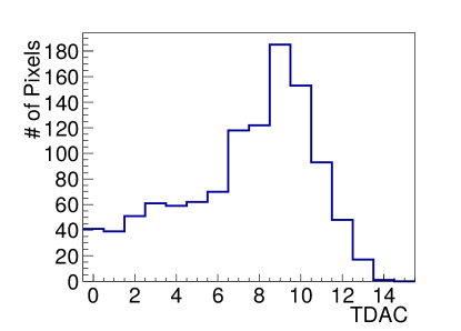
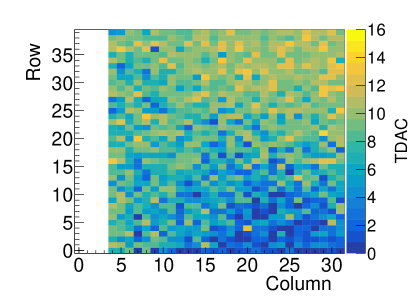
The TDAC values and their distribution over the chip after tuning are shown in figure 8 for three sensors. The TDAC map of the neutron irradiated MuPix (figure 8(b)) looks similar to the TDAC map for a non-irradiated MuPix (figure 8(a)). For the proton irradiated sensors (figure 8(c)) a non-uniform distribution of the TDACs is obtained which we attribute to a non-uniform irradiation beam profile. The observed non-uniform radiation damage causes position dependent depletion and varying noise levels [17]. The distribution of the TDAC values (figure 8(c)) has a shoulder towards lower values which originate from the bottom right part of the TDAC map where the irradiation beam center was probably located 888Dosimetry results of the facility suggest a 10% dose variation over the sensor..
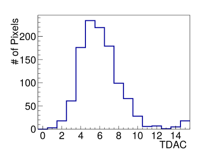
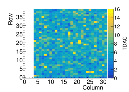
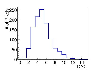
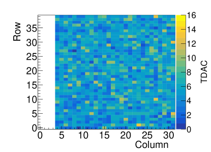
The inhomogeneous proton irradiation prevented us from optimally tuning the sensors, thus compromising the following characterization studies.
4.2 Test beam results
Two MuPix telescopes [14] are used as tracking reference for a test beam performed at the M1 beam line at PSI in November 2016. One telescope is used to characterize the proton irradiated MuPix, see figure 3. The other telescope is used to characterize the neutron irradiated MuPix.
The M1 beam consists of a mixture of , , and protons, with being the dominant beam component. The momentum is set to to select minimum ionizing , which are expected to produce 1200 primary electrons in the depletion zone of a non-irradiated MuPix7 sensor at a depletion voltage of . The particle rate of the beam is set to about of which only about are reconstructed by the telescopes due to limited acceptance. Both MuPix telescopes are mechanically aligned with a precision of better than relative to each other. A software alignment procedure is applied to correct for residual offsets with a precision of .
Efficiency and noise study
To study efficiency and noise, reference tracks are extrapolated to the DUT. On the DUT, clustering and crosstalk removal is applied. A search window of radius and a time window of around the extrapolated track intersection is used to match hit clusters. The hit finding efficiency is defined as the number of matched tracks divided by the total number of extrapolated tracks and corrected for random coincidences. The quoted efficiencies include all components of the readout system: hit digitization, on-chip readout state machine, data transmission over the serial link and front-end processing on the readout FPGA, i.e. time stamp sorting and merging of data from the four telescope layers.
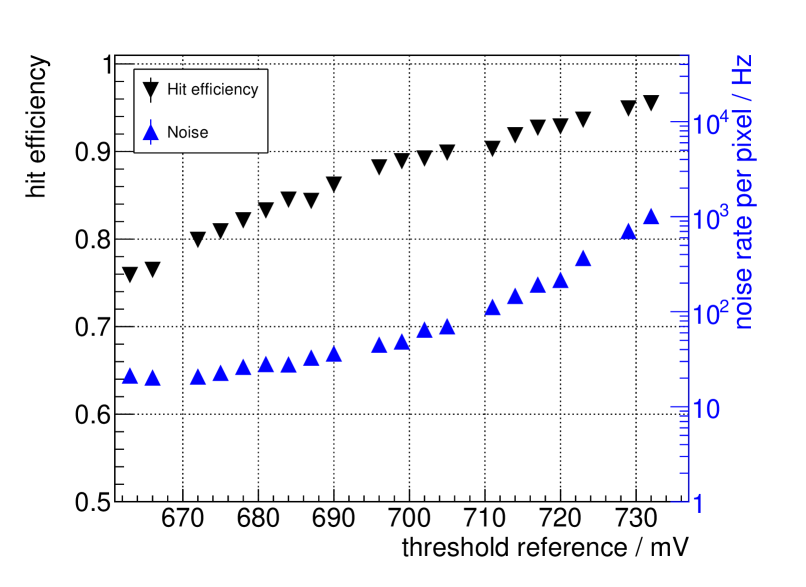
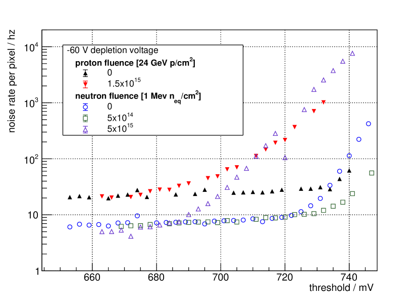
Figure 9 shows exemplary results for the efficiency and noise of the tested samples as a function of the applied threshold reference. The noise consists of all unmatched clusters and is corrected for small inefficiencies of the reference planes. Due to the small size of the sensors in the reference planes (about 1/10 of the beam profile) and large angle scatterers a significant fraction of beam particles entering the DUT cannot be reconstructed. This adds a constant noise floor of about () for the proton (neutron) irradiated sensors.
The noise of the neutron irradiated sensor is similar to the non-irradiated sensor: up to a reference threshold of about the noise stays below ; for higher threshold references (lower thresholds) the noise increases exponentially.
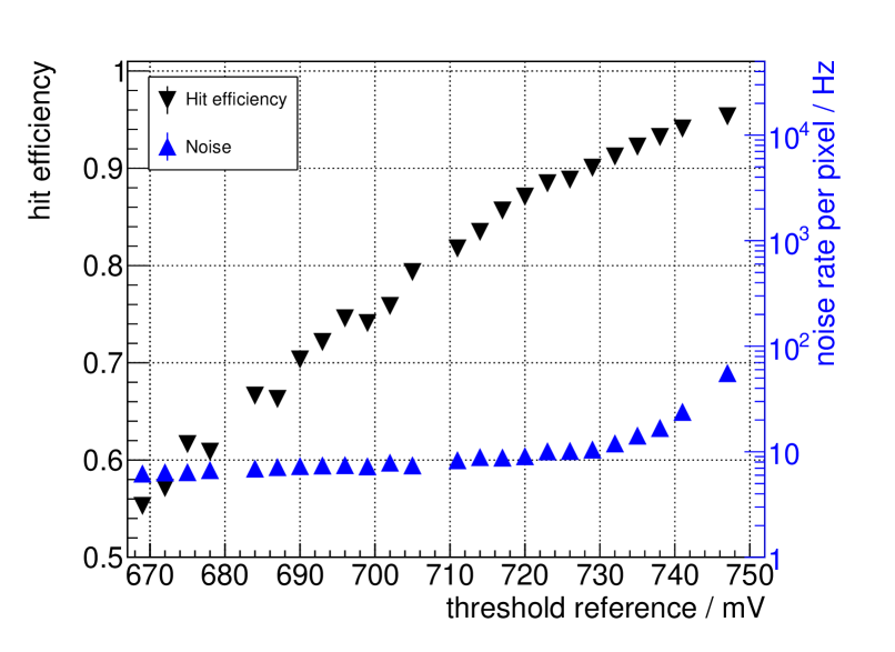
The noise of the proton irradiated sensor increases more rapidly and already starts at low reference threshold (high thresholds). Proton and neutron irradiated sensors with a depletion voltage of reach efficiencies of about , similar to the non-irradiated sensor, however, at the expense of factor 10-100 higher noise levels and increased leakage currents. Higher efficiencies can be reached by further increasing the depletion-voltage.
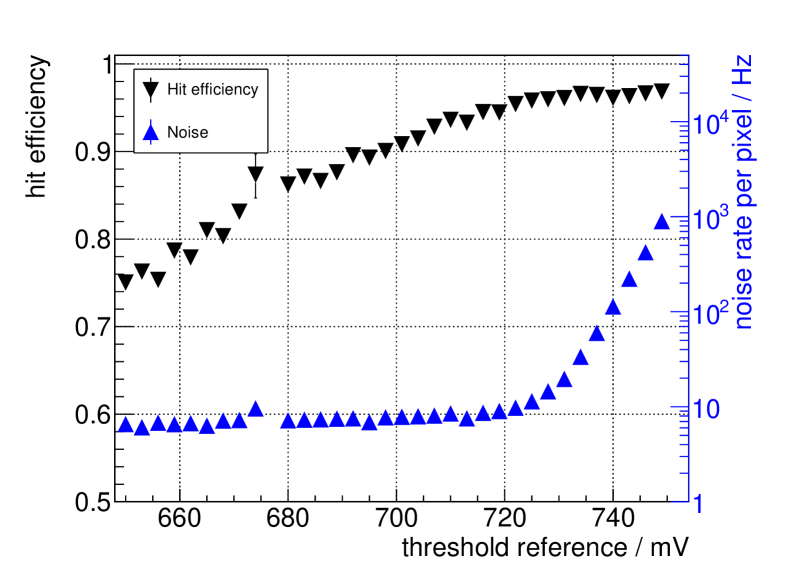
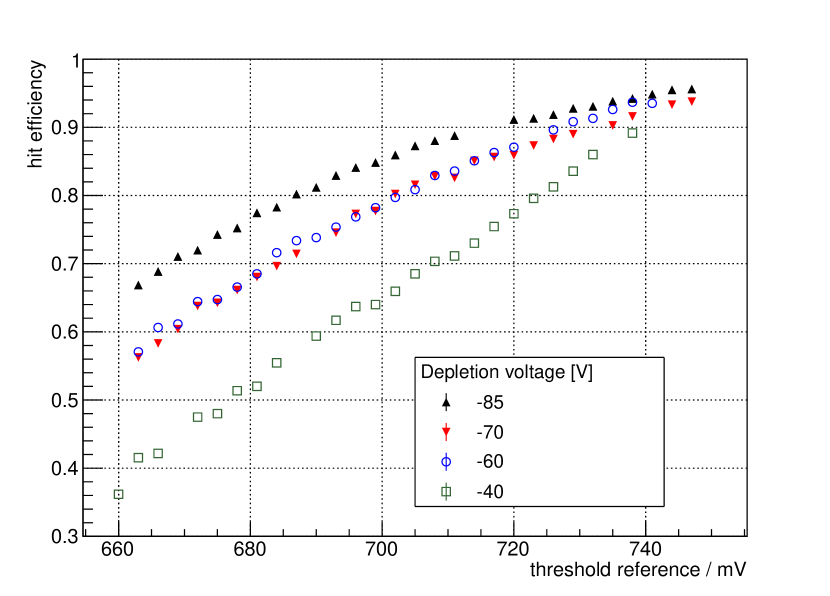
The influence of the depletion voltage on the efficiency and noise as a function of the threshold reference is shown in figure 10 for a neutron irradiated sensor with which was operated at a sensor temperature of about . The sensor efficiency increases with the applied depletion voltage, consistent with the expectation that the active depletion zone grows proportional to , leading to higher signals. At very high negative voltages additional avalanche effects contribute to charge amplification, which sets in at about for non-irradiated sensors and shifts to slightly higher negative voltages for irradiated sensors [17]. For a depletion voltage of an efficiency of about is measured at a threshold reference of and a noise rate of about per pixel. The noise significantly increases for larger threshold references. The shift of the threshold curves for the different depletion voltages can be explained by tuning effects: different VPDAC values and tune thresholds are used for the and measurements compared to the and measurements, as seen in table 2. This results in a shift of the effective threshold by about .
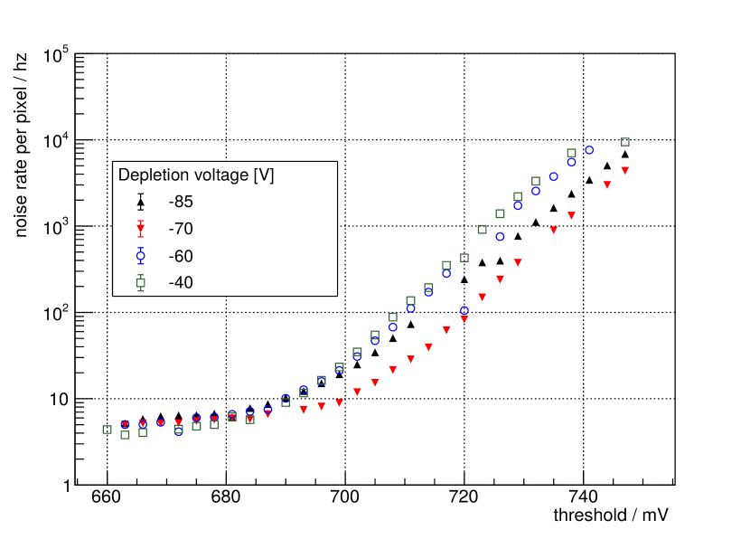
For the different irradiated samples the efficiency and noise measurements are summarized in figure 11 as a function of threshold value. Data samples with a common, but reduced, HV of are chosen here to allow for a systematic comparison of all irradiated sensors999Sensor N514 was accidentally damaged after taking data at .. Small differences in the efficiency are expected from the different telescope geometries: The neutron irradiated samples are glued on a carrier and placed behind the three reference layers. They have by to reduced efficiencies due to undetected particle losses with large angle scattering in the third layer.
In general, neutron and proton irradiated samples show similar performance, considering the threshold variations due to different VPDAC settings and the limited threshold scan for the neutron-irradiated sensor which does not reach very low effective thresholds. Accounting for these differences the data show overall an efficiency loss and noise increase for increasing neutron and proton fluences. Although the MuPix irradiated to reaches almost similar efficiencies than the non-irradiated one, it shows a significant noise increase. At very low threshold reference values (high threshold) a beam induced noise floor of and is measured for the proton and neutron irradiated sensors, respectively.
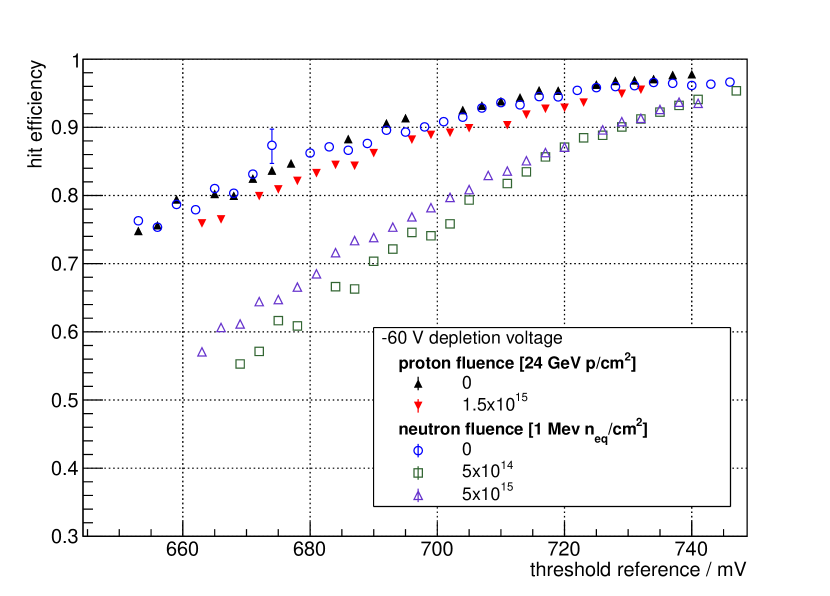
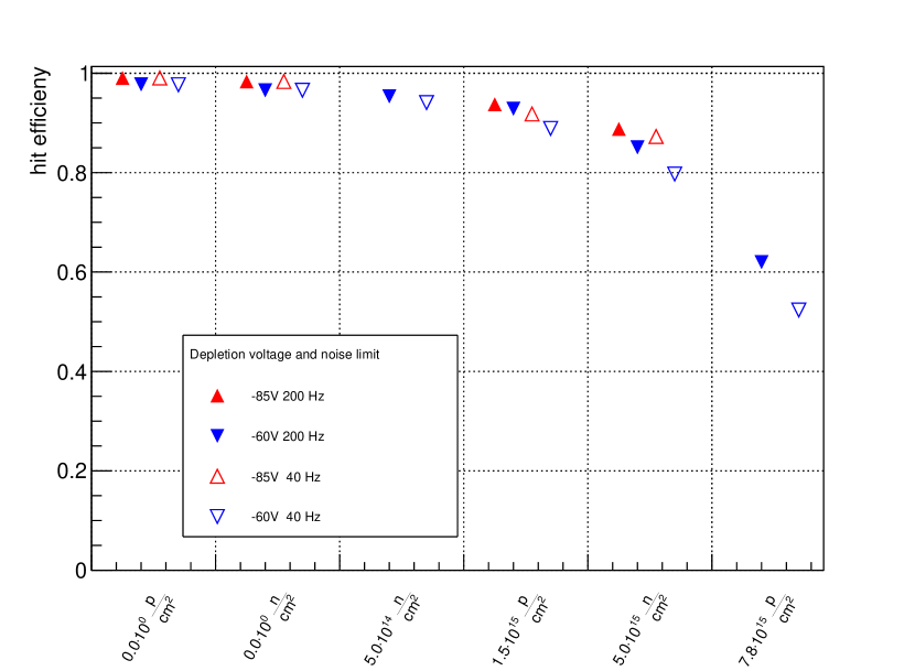
The automated threshold tuning procedure leads to strong correlations between the efficiency and noise measurements and the threshold used for tuning, also visible as shifts of the threshold curves in figures 10 and 11. To compare the different samples in a more setting independent way, the efficiencies are determined for fixed average noise rates of () per pixel101010For LHC experiments noise occupancies are typically required to be below , corresponding to noise per pixel at bunch crossing frequency.. The noise floor of () for the neutron (proton) irradiated samples is subtracted. The resulting efficiencies are shown in figure 12 for depletion voltages of and . The efficiencies of the proton- and neutron-irradiated sensors show a moderate reduction up to a fluence of . For higher fluences the efficiency decreases more strongly and falls below 90 %. The efficiency difference between the average per pixel noise rates of and indicates the possible efficiency gain if the sensors are cooled to even lower temperatures.
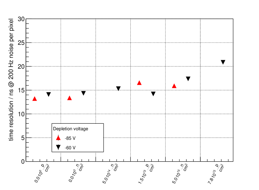
Time resolution
The time resolution of the MuPix7 DUT is measured relative to the averaged time stamps of the hits from reference tracks. A Gaussian fit is applied to a histogram of the time differences. The standard deviation, , of the fit defines the time resolution, which is corrected for the limited resolution of the reference sensors
| (1) |
assuming a time resolution of for the non-irradiated MuPix7 [10, 11]. Using the time resolution of the DUT is measured for all MuPix and for different depletion voltages, see figure 13. The time resolution of the non-irradiated MuPix of about is in agreement with previous measurements [10]. It stays constant for fluences up to and is also rather independent of the threshold setting and therefore the noise limit. For higher proton and neutron fluences, the time resolution of the sensor becomes significantly worse.
5 Conclusion
Proton and neutron irradiated samples of HV-MAPS prototypes with a particle fluence of up to were tested in the laboratory and at a PSI test beam. All sensors are fully functional after one year of annealing at room temperature.
The MuPix7 samples have a non-radiation-hard design and were realized on a substrate with a depletion zone of at a depletion voltage before irradiation. For the irradiated samples increased noise rates and leakage currents in the pixel matrix are observed. The proton irradiated samples show significantly higher leakage currents as the neutron irradiated sensors for similar particle fluences in the laboratory.
At PSI, efficiency and noise studies with sensors cooled down to have been carried out. At an optimal depletion voltage of and at a maximum noise limit of efficiencies are measured for all sensors with a dose of up to . For higher proton and neutron fluences a significant performance degradation is observed. The time resolution for all irradiated sensors is below , compared to about time resolution of the non-irradiated references. Only a small time resolution decrease for fluences of up to is observed. During full operation in the test beam the overall noise seems to be strongly influenced by bulk damage induced charge trapping.
Despite the non-radiation-hard design and the very small depletion zone of the standard AMS H18 process, the MuPix7 shows high radiation tolerance emphasizing the potential of the AMS H18 process for usage in harsh radiation environments. The radiation tolerance of the synthesized and fast readout state machine logic is demonstrated for the first time for a fully monolithic prototype realized in HV-CMOS technology.
Acknowledgments
N. Berger and D. vom Bruch thank the Deutsche Forschungsgemeinschaft for supporting them and the Mu3e project through an Emmy Noether grant. S. Dittmeier and L. Huth acknowledge support by the IMPRS-PTFS. A.-K. Perrevoort acknowledges support by the Particle Physics beyond the Standard Model research training group [GRK 1940]. H. Augustin and A. Herkert acknowledge support by the HighRR research training group [GRK 2058]. N. Berger thanks the PRISMA Cluster of Excellence for support. This project was also supported by BMBF grant 05H15VHCA1. We would like to thank PSI for valuable test beam time. The authors gratefully acknowledge the support by the CERN PS and SPS instrumentation team and would like to sincerely thank Prof. Dr. V. Cindro and the team of the TRIGA reactor in Ljubljana for performing neutron irradiations for this publication.
References
- [1] I. Perić, “A novel monolithic pixelated particle detector implemented in high-voltage CMOS technology”, Nucl.Instrum.Meth., A582 876, 2007.
- [2] AMS AG, Tobelbader Strasse 30, 8141 Unterpremstaetten (Austria).
- [3] M. Benoit et. al, “Results of the 2015 testbeam of a 180 nm AMS High-Voltage CMOS sensor prototype”, Journal of Instrumentation, 11(07) P07019, 2016.
- [4] M. Benoit et al., “Testbeam results of irradiated ams H18 HV-CMOS pixel sensor prototypes”, https://arxiv.org/abs/1611.02669, 2016.
- [5] H. Pernegger et al., “First tests of a novel radiation hard CMOS sensor process for Depleted Monolithic Active Pixel Sensors”, Journal of Instrumentation, 12(06) P06008, 2017.
- [6] A. Blondel et al., “Research Proposal for an Experiment to Search for the Decay ”, https://arxiv.org/pdf/1301.6113.pdf, 2013.
- [7] “Webpage of the PS Irradiation Facility ”, (online, accessed 2018-03-20, https://ps-irrad.web.cern.ch.
- [8] L. Snoj, G. Zerovnik and A. Trkov, “Computational analysis of irradiation facilities at the JSI TRIGA reactor”, Appl. Radiat. Isot. 70 (2012) 483., 2016.
- [9] H. Augustin et al., “The MuPix system-on-chip for the Mu3e experiment”, Nucl.Instrum.Meth., A845 194 – 198, 2017, Proceedings of the Vienna Conference on Instrumentation 2016.
- [10] H. Augustin et al., “MuPix7 - A fast monolithic HV-CMOS pixel chip for Mu3e”, Journal of Instrumentation, 11(11) C11029, 2016.
- [11] H. Augustin et al., “Efficiency and timing performance of the MuPix7 high-voltage monolithic active pixel sensor”, https://arxiv.org/abs/1803.01581, submitted to Nucl.Instrum.Method-A, 2018.
- [12] K.-L. Simmoteit, “Development of an X-Ray based Energy Calibration Method for High Voltage Monolithic active Pixel Sensors”, Bachelor thesis, Heidelberg University, Physics Institute, https://www.psi.ch/mu3e/ThesesEN/BachelorSimmoteit.pdf, 2017.
- [13] I. Mateu, ”NIEL hardness factor determination for the new proton irradiation facility at CERN”, talk at the 28th RD50 workshop in Torino: https://cds.cern.ch/record/2162852/files/AIDA-2020-SLIDE-2016-002.pdf (online, accessed 2018-04-30), 2016.
- [14] H. Augustin et al., “The MuPix Telescope: A Thin, High-Rate Tracking Telescope”, Journal of Instrumentation, 12(01) C01087, 2017.
- [15] Labfacility Pt1000: Datasheet (http://www.farnell.com/datasheets/1918818.pdf?_ga=2.73347419.911411872.1496222551-845443501.1496222551, online, accessed 2017-05-30).
- [16] M. Fernández García, C. Gallrapp, M. Moll and D. Muenstermann, “Radiation hardness studies of neutron irradiated CMOS sensors fabricated in the ams H18 high voltage process”, Journal of Instrumentation, 11(02) P02016, 2016.
- [17] Affolder et al., “Charge collection studies in irradiated HV-CMOS particle detectors”, Journal of Instrumentation, 11(04) P04007, 2016.