The electroluminescent properties based on bias polarity of the epitaxial graphene/aluminium SiC junction
Abstract
We investigated the electroluminescent properties of the epitaxial graphene/SiC junction. The temperature and current dependence of electroluminescence from the epitaxial graphene/SiC is measured within a temperature range of 50-300 K. The result of electroluminescence at 300 K is compared with the electroluminescent spectra from aluminium/SiC junction. The difference between the spectra is explained by the different band bending, which could lead to the tunable LED due to the semi-metal character of the graphene. We observed the electroluminescence at both bias polarities and we described the blue shift in the spectra by Franz-Keldysh effect.
Silicon carbide is a material with an indirect broad bandgap from 2.3 to 3.3 eV depending on the SiC polytype. The unique properties of SiC, such as high saturation velocity of charge carriers or high thermal conductivity, make it a promising candidate for high-power and high-temperature applications. Casady and Johnson (1996).
The first LED was made of SiC material in 1927 Zheludev (2007). Jan et al. Jan et al. (2009) investigated blue electroluminescence from an SiC tunneling diode. Strong electroluminescence in blue range was observed by Lebedev et al. Lebedev and do Carmo (1997). Kamiyama studied the extremely high quantum efficiency of donor-acceptor-pair emission between nitrogen (donor) - boron (acceptor) and nitrogen - aluminium (acceptor) in SiC in a range of yellow and blue color Kamiyama et al. (2006), which makes SiC suitable for the production of white LED with a very high color rendering index. Ou et al. (2014) The color rendering index is a quantitative measure of the ability of a light source to reveal the colors of various objects faithfully in comparison with an ideal or natural light source. Optical emission between N and B has a wavelength at nm with full width at half maximum (FWHM) nm and between N and Al has a wavelength at nm with FWHM nm. Another prospective use of SiC is in the area of room temperature single photon emitters Fuchs et al. (2013).
Graphene is a two-dimensional crystal, consisting of a hexagonal lattice of carbon atoms. One of the methods of graphene growth is a thermal decomposition of SiC. The graphene layer is formed on the SiC surface. This growth method provides, besided chemical vapour deposition, the highest figure of merit in terms of graphene quality and scalability, the two requirements for applications in electronics and optoelectronics Kunc et al. (2014); Dong et al. (2014); Berger et al. (2004). There has been both intense theoretical Inoue et al. (2012); Kageshima et al. (2013) and experimental Ohta et al. (2010); Sun et al. (2011); Borysiuk et al. (2012); Ostler et al. (2013) research of graphene/SiC interface. However, detailed studies of electroluminescent properties of graphene/SiC interface are rare Anderson et al. (2012).
We have studied electroluminescent (EL) properties of the graphene/SiC LED at different temperatures (50-300 K). We compared the results of an etalon sample with an Al/SiC interface and discussed differences of electrooptical properties. We verified in comparison with aluminium contacts, that the electroluminescence can be altered by different electron affinity of graphene. The altered EL emission is a fingreprint of surface-related electron-hole recombination. We show, employing graphene semimetalicity and low density of states, can be used for applications in tunable EL diodes. We present a theory based on the change of the bangap with the high electric inner field which explains the observed EL shift depending on the applied voltage.
We grew graphene on a Si-face of the conductive SiC 4H polytype (manufactured by II-VI Incorporation) by thermal decomposition of SiC at 1650∘C for 5 minutes in an argon atmosphere. SiC substrate was doped by nitrogen ( cm-3) and its dimensions were mm. The presence of graphene on the SiC surface was verified by Raman spectroscopy.
To measure EL the sample was inserted between a copper plate and Teflon tape. An aluminium tip was attached on the graphene layer (Figure 1). The tip and Cu plate were connected to a current source Keithley 2400.
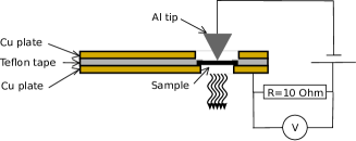
We have measured current-voltage (I-V) characteristics and EL spectra in the temperature range K. The current source was Keithley 2400 which supplied current up to A. Multimeter Keithley 2000 measured voltage () on the resistor . The voltage on the sample is equal to .
The spectrometer Princeton Instruments SpectraPro 2300i with grating 600 lines/mm and cooled CCD detector at a temperature of liquid nitrogen was used to measure the EL spectra. The EL was collected from the opposite side to which the Al tip was attached.
We measured the EL spectrum from the sample with and without graphene contact. These spectra are shown in Figure 2. It is evident that EL was observed in both polarities. The spectra of the sample with and without graphene look similar, but there is a difference between intensity and there is a small shift ( nm), which is caused by a different internal electric field. The internal electric field depends on band bending and on the work function of the metal. This means that if we change the work function of the metal, the EL spectra will change too. Fermi level in graphene is easily controlled by gate voltage because graphene is a semi-metal Yang et al. (2012).
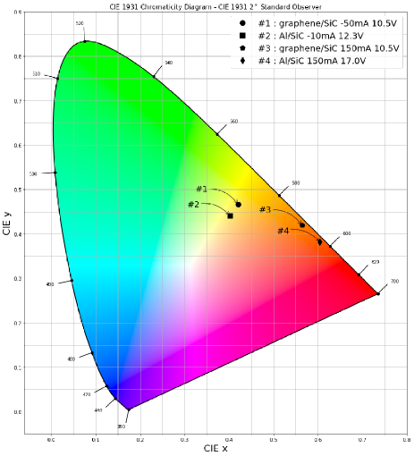
To illustrate the color in both polarities and both contacts the calculated color (CIE x,CIE y)-coordinates are shown on the Commision Internationl de l’Eclaire (CIE) 1931 chromaticity diagram on Figure 3.
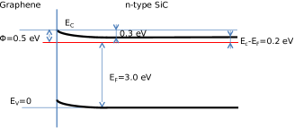
The electron affinities of graphene and SiC are 4.5 and 4.0 eV, respectively Nagashio et al. (2010); Sze and Ng (2007). The 4H-SiC bandgap is 3.23 eV and the Fermi level is located below the conduction band. This means that the work function of SiC ( eV = sum of electron affinity eV and eV energy difference between the bottom of the conduction band and the Fermi energy) is close to the work function of graphene. Therefore, a relatively small band bending upwards can be formed on the interface based on the simple model of work function difference (Figure 4). The band bending of aluminium/SiC interface is 0.1 eV due to the work function of aluminium, which is approximately 4.3 eV.
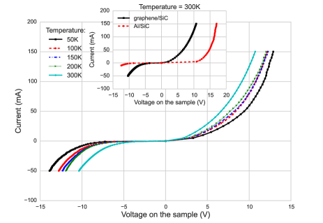
The temperature dependence of the sample I-V characteristic is shown in Figure 5. The I-V curves were measured between mA and mA with a step of mA for negative polarity and mA for positive polarity on Al tip. The maximal voltage on the sample was about V for both current polarities. The current increases as the temperature increases due to the thermally excited electrons over the barrier of the graphene/SiC interface. The insert graph shows the difference between Al and graphene contacts. It is evident that graphene contact allows the carriers to move easily, in bulk, over the barrier.
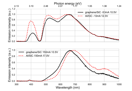
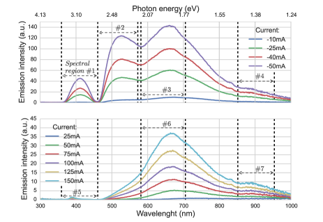
The current dependence of the EL spectrum at K is shown on Figure 6. The top graph shows the EL spectra in negative polarity (negative bias at the Al contact), which consists of four broad bands. at nm ( eV), at nm ( eV), at nm ( eV) and at nm ( eV). The EL radiation was observed by naked eye.
The EL spectra in positive polarity (plus on the Al contact) are shown in the bottom graph on Figure 6. There are three spectral regions, at nm ( eV) with low intensity, broad strong at nm ( eV) and at nm ( eV). The EL spectrum in positive polarity is approximately three times weaker than in negative polarity, but EL light still visible by naked eye.
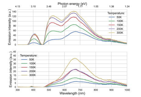
The temperature dependence of EL in forward (current set to 150 mA) and backward (current set to -50 mA) biased junction is plotted in Figure 7. The characteristic temperature dependence leads us to the conclusion that all the radiative transitions are caused by donor-acceptor pairs recombination because the EL intensity decreased with decreasing temperature due to the thermally activated electron-hole recombination between acceptor and donor levels.
The spectral regions at eV and eV are caused by the donor-acceptor transition between N and Al Kalinina et al. (1997); Kuznetsov and Zubrilov (1995). The spectral region at eV is ascribed to donor-acceptor-pair recombination between N donors and Al acceptors levels, too Jan et al. (2009). The transitions between N donors and B acceptors is responsible for EL at eV Kamiyama et al. (2006). The last spectral region at eV could have its origin from a radiative transition between vanadium levels Pavesi et al. (2004) or the transition between energy levels of a silicon vacancy Baranov et al. (2011).
All radiative transitions take place in close proximity to the graphene/SiC interface where the tip is attached because there is the highest voltage gradient. When the negative polarity is applied, the electrons are injected from the graphene to the SiC and they can be trapped at nitrogen levels. The minority holes are drawn from the volume to the interface, where they are captured on the acceptor levels and then they are radiatively recombined with electrons from nitrogen levels.
In applied positive bias, the electrons are injected from the back contact and attracted from volume to the interface. However, the holes are blocked at the interface and pass through the barrier in a small quantity from the graphene. They are immediately trapped on the boron levels, which have greater capture cross section than the other levels. Then the captured holes recombine with electrons bound on nitrogen donors and cause the EL at eV ( nm) with FWHM about eV ( nm).
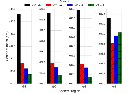
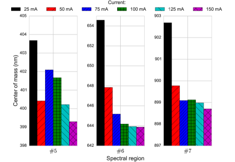
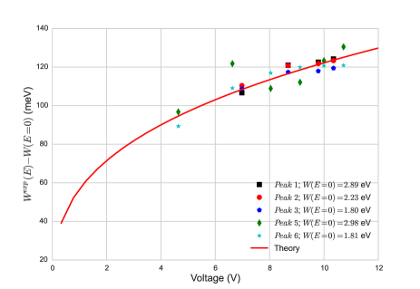
The determined ”band centers of mass” from marked areas in the graph on Figure 6 is listed at Table 1 for reverse polarity and at Table 2 for positive polarity. The ”band centers of mass” show a small blue shift (Figure 8 for reverse polarity and Figure 9 for positive polarity). This shift is caused by the change of the bandgap in dependence on the electric inner field. The maximal electric inner field under interface is described by the formula Sze and Ng (2007)
| (1) |
where is the voltage, is a donor concentration, is the elementary charge and is the absolute permittivity. The electric inner field is shifted in a range of V/m in our case of the applied voltage ( V). The change of the bandgap depending on the electric internal field is described by Franz-Keldysh effect Satzke et al. (1991)
| (2) |
where is the position of ”band centres of mass” without applied bias, is the reduced Planck constant and is the effective mass. The theoretical curve ( cm-3, , ) and experimental data are plotted in graph in Figure 10 and there is a match between experimental data and theory. It means that the position of ”spectral region center of mass” depends on the applied bias.
| Current | Spectral region | |||
|---|---|---|---|---|
| (mA) | ||||
| -10 | 413.79 | 529.82 | 648.95 | 897.32 |
| -25 | 411.83 | 527.48 | 646.05 | 896.81 |
| -40 | 411.61 | 527.26 | 645.86 | 896.97 |
| -50 | 411.38 | 526.91 | 645.35 | 897.03 |
| Current | Spectral region | ||
|---|---|---|---|
| (mA) | |||
| 25 | 403.68 | 654.58 | 902.69 |
| 50 | 400.42 | 647.84 | 899.77 |
| 75 | 402.09 | 645.17 | 899.09 |
| 100 | 401.67 | 644.18 | 899.12 |
| 125 | 400.22 | 643.93 | 898.97 |
| 150 | 399.30 | 643.86 | 898.70 |
In conclusion, the sample produces the EL in both current directions with a different emission spectral range. The observed EL spectra are formed by donor-acceptor transitions, which was confirmed by El intensity dependence on temperature. The blue shift of EL Spectral regions dependence on the bias was explained by the theory based on the change of bandgap due to the high electric inner field. We conclude that the control of the position of Fermi level in graphene by the voltage on the gate electrode can lead to a shift in the color perception of the emitted spectrum.
Acknowledgments
The study was supported by the Charles University, project GA UK No.932216, the Grant Agency of Czech Republic under No. 16-15763Y and SVV-2017-260445. Raman spectroscopy has been measured as part of Project No. VaVpI CZ.1.05/4.1.00/16.0340.
References
- Casady and Johnson [1996] J. Casady and R. Johnson, “Status of silicon carbide (sic) as a wide-bandgap semiconductor for high-temperature applications: A review,” Solid-State Electronics 39, 1409 – 1422 (1996).
- Zheludev [2007] N. Zheludev, “The life and times of the led — a 100-year history,” Nature Photonics vol. 1, 189–192 (2007).
- Jan et al. [2009] S.-R. Jan, T.-H. Cheng, T.-A. Hung, P.-S. Kuo, M. Han Liao, Y. Deng, and C. Wee Liu, “Blue electroluminescence from metal/oxide/6h-sic tunneling diodes,” Electron Devices, IEEE Transactions on, IEEE TRANSACTIONS ON ELECTRON DEVICES 55, 3590 – 3593 (2009).
- Lebedev and do Carmo [1997] A. Lebedev and M. do Carmo, “6h-sic p-n structures with predominate exciton electroluminescence, obtained by sublimation epitaxy,” Materials Science and Engineering: B 46, 275 – 277 (1997), e-MRS 1996 Spring Meeting, Symposium A: High Temperature Electronics: Materials, Devices and Applications.
- Kamiyama et al. [2006] S. Kamiyama, T. Maeda, Y. Nakamura, M. Iwaya, H. Amano, I. Akasaki, H. Kinoshita, T. Furusho, M. Yoshimoto, T. Kimoto, J. Suda, A. Henry, I. G. Ivanov, J. P. Bergman, B. Monemar, T. Onuma, and S. F. Chichibu, “Extremely high quantum efficiency of donor-acceptor-pair emission in n-and-b-doped 6h-sic,” Journal of Applied Physics 99, 093108 (2006).
- Ou et al. [2014] H. Ou, Y. Ou, A. Argyraki, S. Schimmel, M. Kaiser, P. Wellmann, M. Linnarsson, V. Jokubavicius, J. Sun, R. Liljedahl, and M. Syvajarvi, “Advances in wide bandgap sic for optoelectronics,” The European Physical Journal B 87, 58 (2014), 10.1140/epjb/e2014-41100-0.
- Fuchs et al. [2013] F. Fuchs, V. A. Soltamov, S. Väth, P. G. Baranov, E. N. Mokhov, G. V. Astakhov, and V. Dyakonov, “Silicon carbide light-emitting diode as a prospective room temperature source for single photons,” Scientific Reports vol. 3, – (2013).
- Kunc et al. [2014] J. Kunc, Y. Hu, J. Palmer, Z. Guo, J. Hankinson, S. H. Gamal, C. Berger, and W. A. de Heer, “Planar edge schottky barrier-tunneling transistors using epitaxial graphene/sic junctions,” Nano Letters 14, 5170–5175 (2014), pMID: 25115623, http://dx.doi.org/10.1021/nl502069d .
- Dong et al. [2014] R. Dong, Z. Guo, J. Palmer, Y. Hu, M. Ruan, J. Hankinson, J. Kunc, S. K. Bhattacharya, C. Berger, and W. A. de Heer, “Wafer bonding solution to epitaxial graphene–silicon integration,” Journal of Physics D: Applied Physics 47, 094001 (2014).
- Berger et al. [2004] C. Berger, Z. Song, T. Li, X. Li, A. Y. Ogbazghi, R. Feng, Z. Dai, A. N. Marchenkov, E. H. Conrad, P. N. First, and W. A. de Heer, “Ultrathin epitaxial graphite: 2d electron gas properties and a route toward graphene-based nanoelectronics”The Journal of Physical Chemistry B 108, 19912–19916 (2004), http://dx.doi.org/10.1021/jp040650f .
- Inoue et al. [2012] M. Inoue, H. Kageshima, Y. Kangawa, and K. Kakimoto, “First-principles calculation of -layer graphene-like growth of c on sic(0001),” Phys. Rev. B 86, 085417 (2012).
- Kageshima et al. [2013] H. Kageshima, H. Hibino, H. Yamaguchi, and M. Nagase, “Stability and reactivity of steps in the initial stage of graphene growth on the sic(0001) surface,” Phys. Rev. B 88, 235405 (2013).
- Ohta et al. [2010] T. Ohta, N. C. Bartelt, S. Nie, K. Thürmer, and G. L. Kellogg, “Role of carbon surface diffusion on the growth of epitaxial graphene on sic,” Phys. Rev. B 81, 121411 (2010).
- Sun et al. [2011] G. F. Sun, Y. Liu, S. H. Rhim, J. F. Jia, Q. K. Xue, M. Weinert, and L. Li, “Si diffusion path for pit-free graphene growth on sic(0001),” Phys. Rev. B 84, 195455 (2011).
- Borysiuk et al. [2012] J. Borysiuk, J. Sołtys, R. Bożek, J. Piechota, S. Krukowski, W. Strupiński, J. M. Baranowski, and R. Stepniewski, “Role of structure of c-terminated -sic() surface in growth of graphene layers: Transmission electron microscopy and density functional theory studies,” Phys. Rev. B 85, 045426 (2012).
- Ostler et al. [2013] M. Ostler, I. Deretzis, S. Mammadov, F. Giannazzo, G. Nicotra, C. Spinella, T. Seyller, and A. La Magna, “Direct growth of quasi-free-standing epitaxial graphene on nonpolar sic surfaces,” Phys. Rev. B 88, 085408 (2013).
- Anderson et al. [2012] T. Anderson, K. Hobart, L. Nyakiti, V. Wheeler, R. Myers-Ward, J. Caldwell, F. Bezares, G. Jernigan, M. Tadjer, E. Imhoff, A. Koehler, D. Gaskill, J. Eddy, C.R., and F. Kub, “Investigation of the epitaxial graphene/p-sic heterojunction,” Electron Device Letters, IEEE 33, 1610–1612 (2012).
- Yang et al. [2012] H. Yang, J. Heo, S. Park, H. J. Song, D. H. Seo, K.-E. Byun, P. Kim, I. Yoo, H.-J. Chung, and K. Kim, “Graphene barristor, a triode device with a gate-controlled schottky barrier,” Science (2012), 10.1126/science.1220527.
- Nagashio et al. [2010] K. Nagashio, T. Nishimura, K. Kita, and A. Toriumi, “Contact resistivity and current flow path at metal/graphene contact,” Applied Physics Letters 97, 143514 (2010), http://dx.doi.org/10.1063/1.3491804 .
- Sze and Ng [2007] S. Sze and K. K. Ng, Physics of semiconductor devices, 3rd ed., 136-139 (Wiley-Interscience, Hoboken, N.J., 2007).
- Kalinina et al. [1997] E. Kalinina, G. Kholujanov, A. Zubrilov, D. Tsvetkov, M. Vatnik, V. Soloviev, V. Tretjakov, H. Kong, and V. Dmitriev, “Effect of ion doping on the electrical and luminescent properties of 4h-sic epitaxial p-n junctions,” Materials Science and Engineering: B 46, 259 – 262 (1997).
- Kuznetsov and Zubrilov [1995] N. Kuznetsov and A. Zubrilov, “Deep centers and electroluminescence in 4h-sic diodes with a p-type base region,” Materials Science and Engineering: B 29, 181 – 184 (1995).
- Pavesi et al. [2004] M. Pavesi, M. Manfredi, P. L. Rigolli, N. Armani, and G. Salviati, “Optical characterization of radiative deep centres in 6h–sic junction field effect transistors,” Semiconductor Science and Technology 19, 45 (2004).
- Baranov et al. [2011] P. G. Baranov, A. P. Bundakova, A. A. Soltamova, S. B. Orlinskii, I. V. Borovykh, R. Zondervan, R. Verberk, and J. Schmidt, “Silicon vacancy in sic as a promising quantum system for single-defect and single-photon spectroscopy,” Phys. Rev. B 83, 125203 (2011).
- Satzke et al. [1991] K. Satzke, H. G. Vestner, G. Weiser, L. Goldstein, and A. Perales, “Electroabsorption studies on InGaAs/InGaAsP quantum-well laser structures” Journal of Applied Physics 69, 7703–7710 (1991), http://dx.doi.org/10.1063/1.347543 .