Probing the phase diagram of cuprates with YBa2Cu3O7-δ thin films and nanowires
Abstract
We have grown and characterized 30 nm thick YBa2Cu3O7-δ (YBCO) films, deposited by pulsed laser deposition on both MgO (110) and SrTiO3 (001) substrates, which induce opposite strain to the superconducting layer. By carefully tuning the in-situ post-annealing oxygen pressure, we achieved, in a reproducible way, films at different oxygen doping, spanning from the slightly overdoped down to the strongly underdoped region of the phase diagram. The transport properties of the films, investigated through resistance versus temperature measurements, are in perfect qualitative agreement with single crystals. Starting from these films, we have also successfully fabricated nanowires with widths down to 65 nm, at different oxygen doping. The nanostructures exhibit characteristic temperatures (as the critical temperature and the pseudogap temperature ) similar to those of the as-grown films and carry critical current densities close to the critical depairing value, limited by vortex entry. This implies that the superconducting and the normal state properties of underdoped YBCO are preserved in our films, and they can be studied as a function of the dimensionality of the system, down to the nanoscale.
pacs:
I Introduction
The microscopic origin of the superconducting phenomenon in High critical Temperature Superconductors (HTSs) is intimately related to the nature of the highly unconventional normal state, which is described by a very complex phase diagram. The still elusive pseudogap state, in the underdoped region of the cuprates, hosts several nanoscale orders, as the newly emerged charge density waves (CDW) Ghiringhelli et al. (2012); Chang et al. (2012); da Silva Neto et al. (2015) and the electronic nematicity Cyr-Choinière et al. (2015); Sato et al. (2017). These two orders break the spontaneous rotational and/or translational symmetry of the crystal. The electronic nematicity causes an anisotropy of the electron transport, which adds to the transport anisotropy due to the orthorhombicity of the crystals Ando et al. (2002). Remarkably, when observed in thin films, it strongly depends on the strain induced by the substrate to the thin film Wu et al. (2017). The strain control in thin films can therefore be instrumental to understand the entanglement between various orders. This requires the growth of thin films, as a function of the oxygen doping, which can well reproduce the main features of the HTS phase diagram.
However, up to now in literature a complete phase diagram is available only for single crystals Ando et al. (2004); Barišić et al. (2013); Hücker et al. (2014). For thin films the strain induced by the substrate has been reported to affect the critical temperature . For instance, for the La2-xSrxCuO4 and La2-xBaxCuO4 compounds a compressive strain causes the complete disappearance of the anomaly, corresponding to the suppression around the doping (where represents the number of holes for planar copper atom). It also leads to a change in the temperature dependence of the resistance above with respect to single crystals Sato et al. (2000a, b). Tensile strain appears instead to be responsible for a strong reduction of at any doping, together with a weakening of the anomaly Sato et al. (2001). Similarly, works on YBa2Cu3O7-δ (YBCO) thin films are rather limited. The presence of the peculiar depression of at is sometimes reported Ye and Nakamura (1993); Wu et al. (1998). However structural disorder and strain, preventing oxygen ordering, have more often led to the disappearance of this feature Osquiguil et al. (1992); MacManus-Driscoll et al. (1994); Tolpygo et al. (1996); Farnan et al. (2000, 2001). The reproducible observation of the anomaly in the phase diagram of thin films is therefore the first step one needs to take to disclose the intertwining of different orders by using nanoscale devices.
Few works are devoted to the fabrication of underdoped nanostructures. Bonetti et al Bonetti et al. (2008) reports on the fabrication of underdoped YBCO nanowires, with widths down to 200 nm. The of the nanowires is 5-10 K lower than that of the unpatterned films, which is already a sign of the degradation of the superconducting properties. Moreover nanowires, patterned on underdoped films having lower than 75 K, are not superconducting. Carillo et al Carillo et al. (2012) show the realization of Nd1.2Ba1.8Cu3Oδ nanodevices, starting from films having various , from the maximum of 65 K down to the non-superconducting state. The of sub-micron wires decreases dramatically - by tens of Kelvin - when reducing the width. Structures narrower than 200 nm are not anymore superconducting. Consequently, it is very hard to distinguish and possibly separate change in doping level from disorder, which are both sources of reduction of in nanowires.
So far underdoped HTS cuprates have never been studied at the nanoscale, on dimensions comparable with the CDW correlation length (of the order of few nanometers at the doping).
In this paper we present the transport characterization of YBCO thin films, covering the whole underdoped region of the () phase diagram. We have grown the films on two substrates, (110) MgO and (001) STO, having completely different matching with the YBCO layer, to study the effect of the strain on the electronic properties. The films, independently of the used substrate, reproduce a phase diagram very similar to that of single crystals, including the anomalies associated with CDW order at the doping. The films, protected by a Au capping layer, have been patterned into nanowires, having widths down to 65 nm. At any oxygen doping, the nanowires have a critical current density very close to the theoretical depairing limit, and a critical temperature very close to the as-grown films. These nanowires are therefore an ideal platform to study the rich and complex physics, characterizing the underdoped region of the YBCO phase diagram, at the nanoscale.
II Film deposition
We have deposited 30 nm thick YBCO films on (110) oriented MgO and (001) oriented SrTiO3 (STO) substrates by pulsed laser deposition (heater temperature 760 ∘C, oxygen pressure 0.7 mbar, energy density 1.5 J/cm2). In previous papers Baghdadi et al. (2015); Arpaia et al. (2017a) we have shown that by slowly cooling down (cooling rate 5 ∘C/min) the films after the deposition, at an oxygen pressure of 900 mbar, we promote the full oxidation of the YBCO chains, therefore achieving slightly overdoped films.
To explore the optimally doped and the underdoped regions of the superconducting dome, soon after the deposition each film is cooled down at a post-annealing pressure, lower than the one used to achieve slightly overdoped samples. To ensure the stability of the pressure during the post-annealing, which favors the reproducibility of the results, we have cooled down the films at a constant and continuous oxygen flow: with this procedure we may use pressures down to mbar, with a stability which is guaranteed within mbar (see Table 1 for a list of the postannealing pressures we have used).
Similar experiments are reported in literature: starting from optimally doped films, the oxygen content is reduced ex-situ through a subsequent annealing at low oxygen pressure Osquiguil et al. (1992); Tolpygo et al. (1996); Farnan et al. (2000); Wuyts et al. (1996). In our case, we have chosen an in-situ annealing to achieve a better degree of homogeneity and reproducibility of the results.
We have chosen to work with two different substrates to check if the strain is responsible for any change in the doping dependence of the electronic properties of the YBCO films, similarly to what has been previously shown in other HTS cuprates Sato et al. (2000a, b, 2001). (001) oriented STO substrates are characterized by in plane lattice parameters Å slightly larger than those of bulk YBCO, Å (given by the average of the -axis and -axis parameters): the lattice mismatch leads to strained superconducting films, with a very small tensile stress of the YBCO cell. On the contrary on (110) oriented MgO ( Å, Å) a large in-plane film-substrate mismatch is present ( and along the [0,0,1] and [1,-1,0] MgO directions respectively). Even though the in-plane mismatch should induce a tensile strain to the YBCO cells, an in-plane compressive strain has been previously reported on YBCO Broussard et al. (1998); Baghdadi et al. (2015), probably related to reconstruction of the MgO surface due to annealing at the high temperatures, required to deposit YBCO Wu et al. (1997). YBCO grows twinned, i.e. with a random exchange of the and axis parameters, both on (110) MgO and on (001) STO Schweitzer et al. (1996). This occurs both because of the in-plane symmetries of the substrates, and because of the chosen deposition conditions.
The thickness has been chosen to be 30 nm: the postannealing becomes more effective at thicknesses nm, favoring homogeneous films, with the same oxygen content throughout the thickness.
III Study of the temperature dependence of the resistance
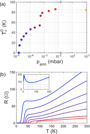
The resistance vs temperature of the films has been measured with the Van der Pauw method Van der Pauw (1958) in the range between 5 and 300 K. By decreasing the postannealing pressure, we have observed a progressive reduction of the zero resistance critical temperature , as expected for underdoped films, achieving superconducting films with down to K (see Fig. 1a,
| (mbar) | (K) | (K) | (K) | (K) | (K) | () | () | (cm) | (K) | (∘) |
|---|---|---|---|---|---|---|---|---|---|---|
| 0 | 0 | 140 | 197 | - | - | 1115 | 1876 | - | 0.39 | |
| 14.9 | 23.7 | 115 | 183 | - | - | 730 | 952 | 8.0 | 0.42 | |
| 25.8 | 33.1 | 102 | 176 | - | - | 567 | 666 | 6.0 | 0.39 | |
| 32.3 | 37.7 | 88 | 167 | - | - | 394 | 422 | 4.5 | 0.42 | |
| 38.5 | 42.5 | 63 | 156 | - | - | 286 | 286 | 5.0 | 0.42 | |
| 46.4 | 49.9 | 64 | 143 | 250 | 7.6 | 190 | 185 | 3.4 | 0.40 | |
| 49.7 | 52.5 | 64 | 142 | 246 | 4.5 | 104 | 103 | 3.1 | 0.41 | |
| 54 | 60.1 | 69 | 125 | 216 | 4.2 | 95 | 102 | 6.0 | 0.43 | |
| 73.1 | 76.3 | - | 116 | 180 | 3.2 | 85 | 100 | 3.9 | 0.40 | |
| 78.8 | 80.6 | - | 108 | 165 | 2.9 | 82 | 100 | 3.7 | 0.45 | |
| 82.5 | 85.9 | - | 112 | 140 | 2.7 | 73 | 95 | 2.9 | 0.42 | |
| 85.9 | 86.9 | - | - | 99 | 1.1 | 68 | 76 | 2.0 | 0.40 | |
| 84.5 | 85.4 | - | - | - | 0.8 | 63 | 65 | 1.7 | 0.42 |
and Table 1).
The good homogeneity of the films is proven by a rather narrow - lower than 5 K in most of the cases - transition broadening (see Table 1).
In Fig. 1b the resistance of several films at different oxygen doping is shown as a function of the temperature. When decreasing the oxygen content, the resistance increases smoothly at first; then it increases much faster in films with K. This feature has been previously seen both in YBCO single crystals and thin films Segawa and Ando (2001); Wuyts et al. (1996), and the threshold, at which such an abrupt change appears (), has been associated to a sudden change in carrier concentration Veal and Paulikas (1991).
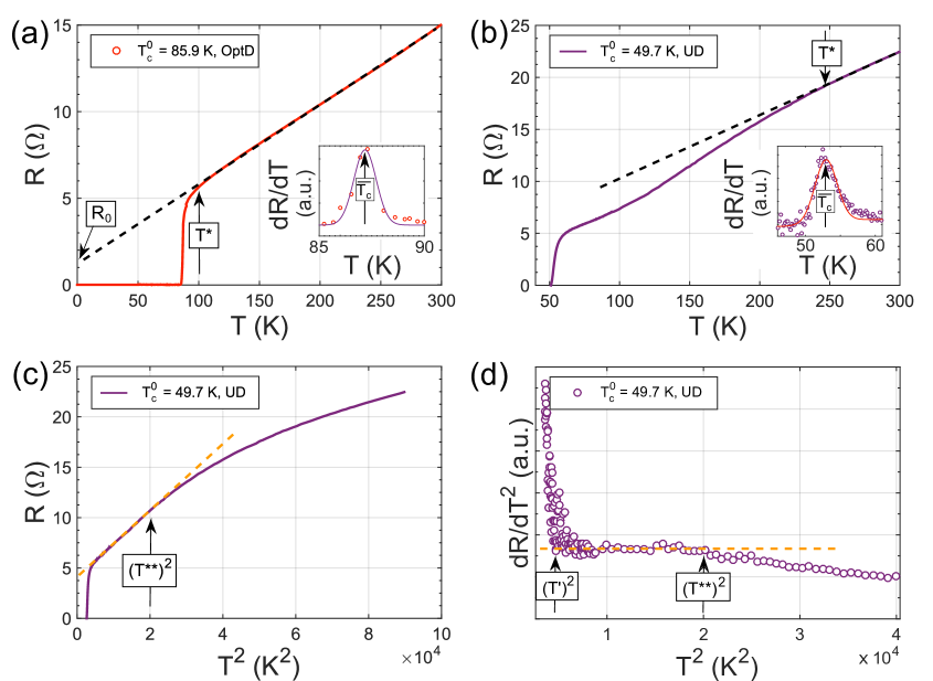
In addition, a clear change in the temperature dependence of the resistance is visible as a function of the doping. The resistance of the films with the highest shows the linear temperature dependence from 300 K down to K, which is typical of optimally doped films (see red curve in Figs. 1b and 2a). When decreasing the oxygen content, the temperature interval in which is linear decreases, and a downward bending develops at lower temperatures. In the more de-oxygenated samples, this downward bending is followed, at even lower temperatures, by an upward bending. Finally, in non-superconducting samples this upward bending is even more pronounced, giving rise to a clear metal-insulator transition (see inset of Fig. 1b) Liu et al. (2004).
In underdoped HTS cuprate single crystals, at least four different characteristic temperatures can be extracted from curves, acting as crossover lines between different regimes and phases Barišić et al. (2013):
-
-
the pseudogap temperature . It represents the crossover line between the pseudogap region and the still poorly understood strange metal phase. Since the latter one is characterized by a linear dependence of the resistance on the temperature, can be inferred by the downward deviation from the -linear behavior.
-
-
the temperature . A crossover from a linear to a purely quadratic resistive behavior can be observed in underdoped films. The temperature represents the upper bound in temperature for the dependence. This temperature linearly decreases when increasing the doping . It is also close to the characteristic temperatures relative to the maximum of the thermoelectric power Cooper and Loram (1996) and the onset of the Kerr rotation signal Kapitulnik et al. (2009). Moreover, below , this temperature has been recently associated to the onset of the nematicity, an in-plane anisotropy in the transport properties of HTS cuprates, appearing in addition to the anisotropy due to the CuO chains, and whose origin is still debated Cyr-Choinière et al. (2015).
-
-
the temperature . It can be inferred from the characteristic as the lower bound in temperature for the dependence. Above , it can be associated with the appearance of superconducting fluctuations, which affect the dc conductivity close to , in agreement with microwave absorption measurements Grbić et al. (2011). The region of superconducting fluctuations is very narrow, though it expands at low doping, where it can extend to more than 20 K above the superconducting transition. Below it has been related to the metal-insulator crossover temperature Liu et al. (2004).
-
-
the critical temperature . It represents the crossover line in the phase diagram below which a superconducting phase appears. Because of the finite broadening of the superconducting transition, a mean critical temperature can be extracted from the maximum of the first derivative of the characteristic.
The extrapolation of the high-temperature linear behavior of the resistance to zero temperature gives the value of the residual resistance . A low value of is the signature of a very clean metallic system, with low disorder. In single crystals it is almost negligible at the optimal doping, while it increases when decreasing the doping Tolpygo et al. (1996); Barišić et al. (2013).
The resistance of our films presents the same dependence on the temperature as observed in single crystals, at all oxygen doping. Hence, we can extract the values of , , and for our thin films. From the fitting of the high-temperature linear behavior of the resistance we have extracted the pseudogap temperature and, by extrapolation to zero temperature, the residual resistance (see Figs. 2a and 2b). Both the pseudogap temperature and increase by reducing the oxygen doping. Nearly optimally doped films present a linear dependence of the resistance on the temperature almost down to the critical temperature ( K); for underdoped films the interval of linearity decreases. In particular, in films having a lower than 46.4 K we do not observe a wide-enough temperature range where the -linear behavior can unambiguously be determined below 300 K, so and cannot be extracted. Underdoped films present instead a purely quadratic resistive behavior at lower temperatures (see Fig. 2c). This Fermi liquid-like dependence of the resistance holds between the two temperatures and (see Fig. 2d). The dependence of the temperature with the oxygen doping is similar to that of the pseudogap temperature, since increases with decreasing of the films. Regarding , it is only few Kelvin higher than at all oxygen doping, except for the strongly underdoped films (), where it increases significantly by reducing the doping. A summary of all the parameters extracted in the most significant samples is listed in Table (1). The of our YBCO thin films as a function of the oxygen doping reproduce the main features of the of single crystals.
IV Structural characterization
The structural properties of the underdoped films have been investigated by Scanning Electron Microscopy (SEM) and X-Ray Diffraction (XRD).
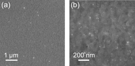
The surface morphology has been determined by SEM images. The YBCO films present at any doping smooth surfaces, characterized by the typical -axis domains with 3D spirals, and an average roughness which is of the order of one atomic cell (see Fig. 3) Arpaia et al. (2017a).
The structural properties have been obtained by XRD analysis. Symmetric scans confirm that the films are highly crystalline and -axis oriented (see Fig. 4a and 4b). Interference fringes, which are an indication of high crystallographic quality Arpaia et al. (2017a), are visible at both sides of the (001) reflection, at all oxygen dopings (see Fig. 4c).
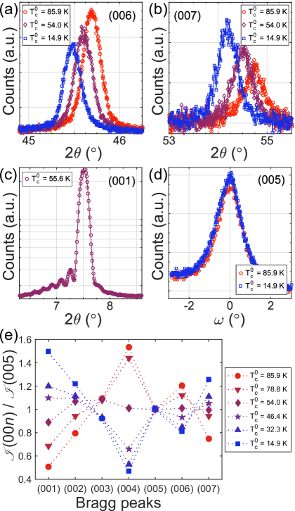
The full width at half maximum (FWHM) of the (0,0,) Bragg peaks, , which is related to the variation of the -axis parameter within each film, and therefore to the order of the crystal structure, is rather small and independent of the oxygen doping (see Table 1).
Asymmetrical maps around the (038)-(308) YBCO reflections (data not shown) confirmed that the films are twinned on both the substrates. The determination of the two in-plane parameters (see Table 2) also led to the confirmation of the strain-state of our films: the YBCO unit cell undergoes an in-plane compressive strain when films are grown on MgO (110) substrates, while the strain is tensile for films grown on STO (001) substrates.
| substrate | (Å) | (Å) | (Å) |
|---|---|---|---|
| MgO (110) | 3.82 | 3.87 | 11.71 |
| STO (001) | 3.84 | 3.90 | 11.67 |
In the whole range of doping the (0,0,) rocking curves have the same FWHM (see Fig. 4d). As a consequence, the doping dependent variation of the broadening of the superconducting transition we have observed cannot be due to structural dishomogeneities or change of crystallinity. In our case is larger for the more underdoped films, and for films having a K (see Table 1). This occurrence could be therefore related to intrinsic properties of the YBCO compound at these doping levels, when various local orders are simultaneously at play.
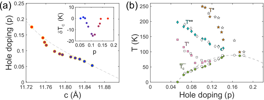
A very significant difference is present in the scans measured on films with different . The reduction of oxygen doping in YBCO is associated to an elongation of the -axis length, which has been observed both in single crystals and in thin films Namgung et al. (1988); Ye and Nakamura (1993). In agreement with that, we have observed that the symmetric (00) Bragg peaks in the XRD scans appreciably shift toward lower diffraction angles (see Fig. 4a and Fig. 4b). The extracted -axis lattice parameters of YBCO are shown as a function of the in Figure 5, for both films grown on (110) oriented MgO substrates (circles) and on (001) oriented STO substrates (triangles).
In case of films grown on STO, the -axis parameter at a given level of doping is smaller than the bulk value, as a consequence of the tensile strain induced by the substrate into the film. The opposite happens in films grown on MgO, where the substrate - whose surface got reconstructed, once it is heated up to the temperatures required for the deposition of YBCO Wu et al. (1997) - induces a compressive strain and the -axis parameter, at a given oxygen doping, is larger than the bulk value. Apart from the change of the -axis length at a fixed oxygen doping, due to the different film/substrate matching, the () behavior we got is independent of the used substrate.
Finally, in agreement with previous results on underdoped YBCO thin films Ye and Nakamura (1993), not only the position, but also the intensity of the (00) Bragg peaks changes with , in opposite directions for different diffraction orders (see Figs. 4a, 4b and 4e) 111The change of the relative intensities of the (00) Bragg peaks is a direct consequence of the structural change of the YBCO unit cell due to the different oxygen content Jorgensen et al. (1990)..
V Doping determination: the thin film phase diagram
To construct the doping () phase diagram, we have to determine for each film the doping .
The experimental determination of in thin films of HTS cuprates is extremely difficult, since it requires the knowledge of the oxygen content , which can be accurately determined only in single crystals. Indeed, in bulk crystals chemical and thermogravimetric analyses, implying the possibility of measuring the mass of the oxygen atoms and its variation as a function of the critical temperature, enable a precise estimate of Beyers et al. (1989).
However, for the specific case of the YBCO compound, the measurement of is very difficult also for single crystals. As a consequence of the crystal structure, one needs to know how holes are arranged between Cu atoms in the CuO2 planes and Cu atoms in the CuO chains, which depends not only on the oxygen content , but also on the degree of oxygen ordering in the chains.
Because of the difficulty in determining , the hole doping is commonly calculated in YBCO single crystals from the critical temperature by using the empirical parabolic relationship
| (1) |
where is the critical temperature at the optimal doping. This equation has been found working well in LSCO, with the exclusion of the data around Takagi et al. (1989); Presland et al. (1991). Consequently, it is inaccurate for determining hole doping around , and it is not applicable for strongly underdoped, not superconducting, samples.
As shown in Ref. Liang et al. (2006), the knowledge of the -axis length in single crystals, in combination with the approximate estimation of given by Eq. 1, allows to establish a unique relation between the values of and .
We have applied the same analysis to YBCO thin films. Figure 5 shows the relation between the -axis parameter and . To determine the relation between the -axis parameter and , we can substitute in this plot each value with the corresponding value (see Table 1). For every , the corresponding doping can be estimated from Eq. 1, considering K, the value of our nearly optimal doped film. The extracted as a function of the -axis lattice parameter is shown in Fig. 6a.
In the interval between and , corresponding to YBCO films with 0 K K, the dependence of the doping on the -axis parameter is linear. The linearity can be extrapolated down to , in the strongly underdoped regime.
At intermediate doping, in the interval between and , corresponding to YBCO films with 40 K K, the data fall below the low doping linear dependence on the -axis value. A possible reason for this deviation at intermediate doping () is the depression of the critical temperature, associated to the presence of charge density wave instability Ghiringhelli et al. (2012); Chang et al. (2012).
From the fit of the data at and (dashed line in Fig. 6a) we can determine the following relationship between and , which is valid in the entire oxygen content range:
| (2) |
where , and Å is the -axis parameter at zero doping. The empirical formula (Eq. 2) is like that found for YBCO single crystals Liang et al. (2006), but with different prefactors. Therefore our data (the independent measurements of and -axis) deviate, similarly to YBCO single crystals, from the parabolic dependence which is instead typically found in YBCO thin films Osquiguil et al. (1992).
The measured values can be plotted as a function of the hole doping , obtained using Equation 2, and compared with those calculated via the parabolic equation (Eq. 1). The difference between the measured and calculated critical temperatures is negligible, except around , where a 16 K (%) suppression of critical temperature is observed (see inset of Fig. 6a). The maximum of the suppression is very similar to the % occurring in LSCO and YBCO single crystals at Takagi et al. (1989); Liang et al. (2006).
Finally, one can plot the four temperatures , , , extracted from the measurements as a function of the hole doping , so to get the () phase diagram of our underdoped YBCO films (see Fig. 6b). This phase diagram is in full qualitative agreement with that of YBCO single crystals Ando et al. (2004); Barišić et al. (2013); Hücker et al. (2014). In addition to that, our result seems to exclude that the strain induced by the substrate may have any role in changing the doping dependence of the electronic properties of our twinned YBCO films, including the depression of the at the doping. Indeed the () data achieved from films deposited both on (110) MgO (filled symbol in Fig. 6b) and on (001) STO (empty symbols in Fig. 6b) substrates fall on top of each other.
VI Underdoped nanowires
To realize underdoped nanowires, we have patterned three 50 nm thick Au capped YBCO films grown on MgO (110): the first one is slightly underdoped, with K; the second one has a doping close to the 1/8 plateau, with K; the third one is strongly underdoped, with K.
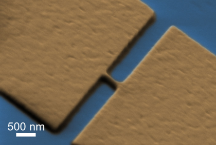
On each of these films, we have fabricated tens of nanowires, with widths down to 65 nm and lengths nm (see Fig. 7). For the nanopatterning, we have used the same procedure, based on an e-beam-lithography-defined carbon mask and a gentle Ar+ ion milling, which we have described in details in our previous works Nawaz et al. (2013a); Arpaia et al. (2013); Nawaz et al. (2013b).
Electrical characterization of the underdoped nanowires has been performed via current-voltage characteristics IVCs and resistance versus temperature measurements. The results of these measurements have been compared with those obtained on slightly overdoped nanowires, having the same geometry, but patterned on a film having K.
At any doping, all the measured nanowires are superconducting. This is a remarkable result, in particular in the strongly underdoped regime, where previous attempts reported in literature were unsuccessful in preserving superconductivity Bonetti et al. (2008); Carillo et al. (2012).
The IVCs measured at K, exhibit a typical flux flow like behavior (see Fig. 8) Arpaia et al. (2014a).

From the IVCs we can determine the critical current of the nanowires, and extract the critical current density . For each sample, we can define a , which is the average of the values extracted within the wire population. The values, reported in Table 3, decrease by two orders of magnitude going from overdoped nanowires to strongly underdoped nanowires.
| doping | (K) | (nm) | (nm) | (A/cm2) | (A/cm2) |
|---|---|---|---|---|---|
| UD | 42.4 | 1000 | 5.0 | ||
| UD | 60.5 | 375 | 5.2 | ||
| UD | 81.4 | 300 | 4.1 | ||
| OD | 85 | 250 | 2.5 |
Such a reduction can be attributed to the change of the zero temperature values of the London penetration depth and of the coherence length , occurring in the underdoped regime. Indeed in 2D nanowires (i.e. characterized, as ours, by dimensions ), the maximum is given by the entry of Abrikosov vortices, driven by the Lorentz force, overcoming the bridge edge barrier Likharev (1979); Papari et al. (2014); Arpaia et al. (2014c). The critical current density due to vortex entry, , can approximately be written as Bulaevskii et al. (2011); Arpaia et al. (2014b):
| (3) |
where is the Ginzburg-Landau depairing critical current density Tinkham (1996)
| (4) |
In the latter equation, depends on and , while is the flux quantum and the vacuum permeability.
In underdoped nanowires, we cannot extract and from the , as we have done on slightly overdoped nanowires Arpaia et al. (2013, 2014b), for reasons which will be clarified later in this section. In single crystals, the dependence of the London penetration depth and of the coherence length on the oxygen doping has been determined by electron-spin resonance measurements and by the values of the upper critical magnetic field respectively Pereg-Barnea et al. (2004); Ramshaw et al. (2012). We can therefore estimate and in our patterned underdoped nanowires, assuming 1) that the values of and at the optimally doped regime are those we have extracted from the fits of the of our slightly overdoped nanowires, considering vortex slip model Arpaia et al. (2014b), and 2) that the dependence of the London penetration depth and of the coherence length on the oxygen doping is the same in single crystals and our nanostructures.
By knowing and , for each underdoped film we can calculate, using Eq. (3), the maximum critical current density that the YBCO nanowires can carry because of vortex entry, , and compare this value with the measured . A summary of all the measured and calculated parameters for the different films at various doping is enclosed in Table 3; the agreement between and is fairly good.
A further confirmation of the quality of the nanowires with different oxygen doping comes from the measurements of the resistance vs temperature , shown in Fig. 9a.
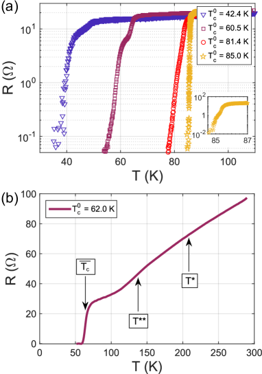
Here, in the geometry we have chosen (see Fig. 7), with the nanowire embedded between two wide electrodes, we see both the superconducting transition of the electrodes, which mostly coincides with that of the as-grown film, and the transition of the nanowire, which is broader and occurs at lower temperature. It is evident that the onset temperature of the superconducting transition related to the nanowire is only a few Kelvin lower than the one of the wide electrodes, independently of the oxygen doping. This circumstance never occurred in previous works on underdoped HTS nanostructures.
The broadening of the superconducting transition associated to the nanowire increases at lower doping, as expected considering dissipation induced by Abrikosov vortices crossing the nanowires Arpaia et al. (2014b), as a consequence of the larger values of and . However, at the moment a quantitative analysis of this transition is still missing. Indeed, the broadening of the transition of the unpatterned underdoped films, which is related to intrinsic properties of the YBCO compound at specific doping levels, influences the transition broadening of the nanowires, possibly giving rise to a substantial contribution which adds to that coming from the entry of Abrikosov vortices.
From the measurement of the critical current density and of the critical temperature, we conclude that the superconducting properties of Au capped YBCO nanowires are unaffected by the nanopatterning procedure. However the electronic properties in the normal state are hidden, since is dominated by the Au capping layer, acting as an electrical shunt Arpaia et al. (2013). To study the physics of the YBCO nanostructures at temperatures larger than the superconducting transition temperature, we have fabricated bare underdoped YBCO nanowires, which are protected during the nanopatterning procedure only by a hard carbon mask, deposited by pulsed laser deposition at room temperature and removed by an oxygen plasma etching at the end of the fabrication. The fabrication of nanowires, unprotected by gold, is slightly detrimental to the superconducting properties 222The reason lays in the thermal conductivity of carbon, which is - differently than Au - much lower than that of YBCO and it cannot prevent the overheating of the superconducting layer during the baking of the resists and the Ar+ ion milling., as we have already investigated in the slightly overdoped region Arpaia et al. (2017b, a). However, from the of these nanowires we can extract, following the procedure described in Section III for thin films, all the temperatures characterizing the phase diagram of YBCO in the normal state (see Fig. 9b).
VII Summary and conclusions
We have succeeded in fabricating and studying high quality YBCO thin films as a function of the oxygen doping, from the slightly overdoped regime down to the strongly underdoped region. The phase diagram we can build, from the analysis of the of the films, has strong analogies with that of YBCO single crystals, both in the superconducting and in the normal state. In particular, the superconducting dome of our thin films is depressed in correspondence of the doping, which is a feature suggestive of a strong competition of superconductivity with the CDW order Ghiringhelli et al. (2012); Chang et al. (2012). The presence of this feature, and more in general the doping dependence on the temperature, characterizing the normal state of the YBCO phase diagram, are not strain dependent: we got identical features on twinned films both deposited on (110) oriented MgO substrates and on (001) oriented STO substrates, where the strain induced into the superconducting layer is respectively compressive and tensile.
We have patterned the thin films into nanowires, both with and without the protection of a Au capping layer. The nanowires, with widths down to 65 nm, are superconducting at any oxygen doping under investigation and preserve essentially the same properties as unstructured films. Nanowires capped with Au are ideal structures to study the superconducting properties at the nanoscale, since they are characterized by values of the critical current densities, close to the depairing values, and of the critical temperatures, close to the as-grown films. The electronic properties in the normal state of the YBCO phase diagram can also be studied in bare nanowires: the dependence of uncapped YBCO nanowires presents indeed signature of all the characteristic temperatures, acting as crossover lines between different regimes and phases.
Our underdoped YBCO nanowires pave the way for several experiments aiming at elucidating the connection between superconductivity and the various nanoscale orders playing a role in the underdoped region of the HTS phase diagram. Ultimately this could lead to a better understanding of the microscopic mechanisms responsible for High critical Temperature Superconductivity.
Acknowledgements.
This work has been supported by the Swedish Research Council (VR) and by the Knut and Alice Wallenberg Foundation. The authors would also like to thank T. Claeson for inspiring discussions.References
- Ghiringhelli et al. (2012) G. Ghiringhelli, M. Le Tacon, M. Minola, S. Blanco-Canosa, C. Mazzoli, N. B. Brookes, G. M. De Luca, A. Frano, D. G. Hawthorn, F. He, T. Loew, M. M. Sala, D. C. Peets, M. Salluzzo, E. Schierle, R. Sutarto, G. A. Sawatzky, E. Weschke, B. Keimer, and L. Braicovich, Science 337, 821 (2012).
- Chang et al. (2012) J. Chang, E. Blackburn, A. Holmes, N. Christensen, J. Larsen, J. Mesot, R. Liang, D. Bonn, W. Hardy, A. Watenphul, M. v. Zimmermann, E. M. Forgan, and S. M. Hayden, Nat. Phys. 8, 871 (2012).
- da Silva Neto et al. (2015) E. H. da Silva Neto, R. Comin, F. He, R. Sutarto, Y. Jiang, R. L. Greene, G. A. Sawatzky, and A. Damascelli, Science 347, 282 (2015).
- Cyr-Choinière et al. (2015) O. Cyr-Choinière, G. Grissonnanche, S. Badoux, J. Day, D. Bonn, W. Hardy, R. Liang, N. Doiron-Leyraud, and L. Taillefer, Phys. Rev. B 92, 224502 (2015).
- Sato et al. (2017) Y. Sato, S. Kasahara, H. Murayama, Y. Kasahara, E.-G. Moon, T. Nishizaki, T. Loew, J. Porras, B. Keimer, T. Shibauchi, et al., Nat. Phys. (2017), 10.1038/nphys4205.
- Ando et al. (2002) Y. Ando, K. Segawa, S. Komiya, and A. Lavrov, Phys. Rev. Lett. 88, 137005 (2002).
- Wu et al. (2017) J. Wu, A. Bollinger, X. He, and I. Božović, Nature 547, 432 (2017).
- Ando et al. (2004) Y. Ando, S. Komiya, K. Segawa, S. Ono, and Y. Kurita, Phys. Rev. Lett. 93, 267001 (2004).
- Barišić et al. (2013) N. Barišić, M. K. Chan, Y. Li, G. Yu, X. Zhao, M. Dressel, A. Smontara, and M. Greven, Proc. Natl. Acad. Sci. 110, 12235 (2013).
- Hücker et al. (2014) M. Hücker, N. B. Christensen, A. Holmes, E. Blackburn, E. Forgan, R. Liang, D. Bonn, W. Hardy, O. Gutowski, M. v. Zimmermann, et al., Phys. Rev. B 90, 054514 (2014).
- Sato et al. (2000a) H. Sato, A. Tsukada, M. Naito, and A. Matsuda, Phys. Rev. B 61, 12447 (2000a).
- Sato et al. (2000b) H. Sato, A. Tsukada, M. Naito, and A. Matsuda, Phys. Rev. B 62, R799 (2000b).
- Sato et al. (2001) H. Sato, M. Naito, A. Tsukada, S. Karimoto, and A. Matsuda, Physica C 362, 186 (2001).
- Ye and Nakamura (1993) J. Ye and K. Nakamura, Phys. Rev. B 48, 7554 (1993).
- Wu et al. (1998) K.-H. Wu, M.-C. Hsieh, S.-P. Chen, S.-C. Chao, J.-Y. Juang, T.-M. Uen, Y.-S. Gou, T.-Y. Tseng, C.-M. Fu, J.-M. Chen, et al., Jpn. J. Appl. Phys. 37, 4346 (1998).
- Osquiguil et al. (1992) E. Osquiguil, M. Maenhoudt, B. Wuyts, and Y. Bruynseraede, Appl. Phys. Lett. 60, 1627 (1992).
- MacManus-Driscoll et al. (1994) J. MacManus-Driscoll, J. Alonso, P. Wang, T. Geballe, and J. Bravman, Physica C 232, 288 (1994).
- Tolpygo et al. (1996) S. K. Tolpygo, J.-Y. Lin, M. Gurvitch, S. Hou, and J. M. Phillips, Phys. Rev. B 53, 12454 (1996).
- Farnan et al. (2000) G. Farnan, M. McCurry, and D. Walmsley, Physica C 341, 2335 (2000).
- Farnan et al. (2001) G. Farnan, M. McCurry, D. Walmsley, Z. Li, and H. Raffy, Supercond. Sci. Technol. 14, 160 (2001).
- Bonetti et al. (2008) J. A. Bonetti, D. S. Caplan, D. J. Van Harlingen, and M. B. Weissman, Phys. Rev. Lett. 93, 087002 (2008).
- Carillo et al. (2012) F. Carillo, G. M. De Luca, D. Montemurro, G. Papari, M. Salluzzo, D. Stornaiuolo, F. Tafuri, and F. Beltram, New J. Phys. 14, 083025 (2012).
- Baghdadi et al. (2015) R. Baghdadi, R. Arpaia, T. Bauch, and F. Lombardi, IEEE Trans. Appl. Supercond. 25, 1100104 (2015).
- Arpaia et al. (2017a) R. Arpaia, D. Golubev, R. Baghdadi, R. Ciancio, G. Dražić, P. Orgiani, D. Montemurro, T. Bauch, and F. Lombardi, Phys. Rev. B 96, 064525 (2017a).
- Wuyts et al. (1996) B. Wuyts, V. Moshchalkov, and Y. Bruynseraede, Phys. Rev. B 53, 9418 (1996).
- Broussard et al. (1998) P. Broussard, M. Wall, and J. Talvacchio, J. Mater. Res. 13, 954 (1998).
- Wu et al. (1997) K. Wu, S. Chen, J. Juang, T. Uen, and Y. Gou, Physica C 289, 230 (1997).
- Schweitzer et al. (1996) D. Schweitzer, T. Bollmeier, B. Stritzker, and B. Rauschenbach, Thin Solid Films 280, 147 (1996).
- Van der Pauw (1958) L. Van der Pauw, Philips Res. Rep. 13, 1 (1958).
- Segawa and Ando (2001) K. Segawa and Y. Ando, Phys. Rev. Lett. 86, 4907 (2001).
- Veal and Paulikas (1991) B. Veal and A. Paulikas, Physica C 184, 321 (1991).
- Liu et al. (2004) Y. Liu, J. Qu, M. Zhu, S. Zhang, S. Feng, and X. Li, Phys. Rev. B 70, 224512 (2004).
- Cooper and Loram (1996) J. Cooper and J. Loram, J. Physique I 6, 2237 (1996).
- Kapitulnik et al. (2009) A. Kapitulnik, J. Xia, E. Schemm, and A. Palevski, New J. Phys. 11, 055060 (2009).
- Grbić et al. (2011) M. S. Grbić, M. Požek, D. Paar, V. Hinkov, M. Raichle, D. Haug, B. Keimer, N. Barišić, and A. Dulčić, Phys. Rev. B 83, 144508 (2011).
- Jorgensen et al. (1990) J. Jorgensen, B. Veal, A. P. Paulikas, L. Nowicki, G. Crabtree, H. Claus, and W. Kwok, Phys. Rev. B 41, 1863 (1990).
- Namgung et al. (1988) C. Namgung, J. Irvine, J. Binks, and A. West, Supercond. Sci. Technol. 1, 169 (1988).
- Note (1) The change of the relative intensities of the (00) Bragg peaks is a direct consequence of the structural change of the YBCO unit cell due to the different oxygen content Jorgensen et al. (1990).
- Beyers et al. (1989) R. Beyers, B. Ahn, G. Gorman, V. Lee, S. Parkin, M. Ramirez, K. Roche, J. Vazquez, T. Gür, and R. Huggins, Nature 340, 619 (1989).
- Takagi et al. (1989) H. Takagi, T. Ido, S. Ishibashi, M. Uota, S. Uchida, and Y. Tokura, Phys. Rev. B 40, 2254 (1989).
- Presland et al. (1991) M. Presland, J. Tallon, R. Buckley, R. Liu, and N. Flower, Physica C 176, 95 (1991).
- Liang et al. (2006) R. Liang, D. Bonn, and W. Hardy, Phys. Rev. B 73, 180505 (2006).
- Nawaz et al. (2013a) S. Nawaz, R. Arpaia, F. Lombardi, and T. Bauch, Phys. Rev. Lett. 110, 167004 (2013a).
- Arpaia et al. (2013) R. Arpaia, S. Nawaz, F. Lombardi, and T. Bauch, IEEE Trans. Appl. Supercond. 23, 1101505 (2013).
- Nawaz et al. (2013b) S. Nawaz, R. Arpaia, T. Bauch, and F. Lombardi, Physica C 495, 33 (2013b).
- Arpaia et al. (2014a) R. Arpaia, M. Ejrnaes, L. Parlato, R. Cristiano, M. Arzeo, T. Bauch, S. Nawaz, F. Tafuri, G. Pepe, and F. Lombardi, Supercond. Sci. Technol. 27, 044027 (2014a).
- Arpaia et al. (2014b) R. Arpaia, D. Golubev, R. Baghdadi, M. Arzeo, G. Kunakova, S. Charpentier, S. Nawaz, F. Lombardi, and T. Bauch, Physica C 506, 165 (2014b).
- Ramshaw et al. (2012) B. Ramshaw, J. Day, B. Vignolle, D. LeBoeuf, P. Dosanjh, C. Proust, L. Taillefer, R. Liang, W. Hardy, and D. Bonn, Phys. Rev. B 86, 174501 (2012).
- Likharev (1979) K. Likharev, Rev. Mod. Phys. 51, 101 (1979).
- Papari et al. (2014) G. Papari, F. Carillo, D. Stornaiuolo, D. Massarotti, L. Longobardi, F. Beltram, and F. Tafuri, Physica C 506, 188 (2014).
- Arpaia et al. (2014c) R. Arpaia, S. Charpentier, R. Toskovic, T. Bauch, and F. Lombardi, Physica C 506, 184 (2014c).
- Bulaevskii et al. (2011) L. Bulaevskii, M. Graf, C. Batista, and V. Kogan, Phys. Rev. B 83, 144526 (2011).
- Tinkham (1996) M. Tinkham, Introduction to superconductivity (Courier Corporation, 1996).
- Pereg-Barnea et al. (2004) T. Pereg-Barnea, P. Turner, R. Harris, G. Mullins, J. Bobowski, M. Raudsepp, R. Liang, D. Bonn, and W. Hardy, Phys. Rev. B 69, 184513 (2004).
- Note (2) The reason lays in the thermal conductivity of carbon, which is - differently than Au - much lower than that of YBCO and it cannot prevent the overheating of the superconducting layer during the baking of the resists and the Ar+ ion milling.
- Arpaia et al. (2017b) R. Arpaia, M. Arzeo, R. Baghdadi, E. Trabaldo, F. Lombardi, and T. Bauch, Supercond. Sci. Technol. 30, 014008 (2017b).