CH3NH3PbI3/GeSe bilayer heterojunction solar cell with high performance
Abstract
Perovskite (CH3NH3PbI3) solar cells have made significant advances recently. In this paper, we propose a bilayer heterojunction solar cell comprised of a perovskite layer combining with a IV-VI group semiconductor layer, which can give a conversion efficiency even higher than the conventional perovskite solar cell. Such a scheme uses a property that the semiconductor layer with a direct band gap can be better in absorption of long wavelength light and is complementary to the perovskite layer. We studied the semiconducting layers such as GeSe, SnSe, GeS, and SnS, respectively, and found that GeSe is the best, where the optical absorption efficiency in the perovskite/GeSe solar cell is dramatically increased. It turns out that the short circuit current density is enhanced and the power conversion efficiency is promoted (to a high value of ) larger than that in a solar cell with only single perovskite layer. The power conversion efficiency can be further promoted so long as the fill factor and open-circuit voltage are improved. This strategy opens a new way on developing the solar cells with high performance and practical applications.
pacs:
05.60.Gg, 72.10.-d, 71.23-kI Introduction
Photovoltaic (PV) devices are used to convert the solar energy into electricity. How to choose appropriate materials is an indispensable issue in design of PV devices. A number of properties are required for candidate PV materials, such as strong optical absorption over a wide range of light wavelength, good collection properties for carriers and low cost in large-scale applications, Reithmaier and so on. Single crystal and polycrystalline Si have dominated the PV industry for long time owing to its mature manufacturing technology and abundant sources. Due to the indirect band gap of Si, the absorption of light has to be mediated by phonon-assisted processes, giving rise to limitations on the efficiency. Therefore, it is highly desired to look for better materials with direct band gap for a replacement of Si in solar cells, and much effort was paid over the years. To name a few, GaAs is a kind of semiconductor with direct band gap and shows good optical properties, and the efficiency in GaAs-based thin-film solar cell has been realized at Moon . However the high price is one of main obstacles to restrict massive applications of GaAs-based solar cells. The polycrystalline CdTe-based solar cell can absorb of the solar spectra with only m thick Asim , but the main obstacle is the toxicity of cadmium, and thus, CdTe is not suitable for a large-scale and green PV application Shah . Organic solar cells have developed rapidly in recent decades due to technical developments of semiconducting polymers Nunzi ; Hoppe , which have many advantages, including low cost materials, high-throughput roll-to-roll production, mechanical flexibility and light weight Zhao , but high stability and long cyclic lifetime are still big challenges. So, the mixed organic-inorganic halide perovskites (CH3NH3PbX3, X=Cl,Br,I) jump into the stage and become booming PV materials in short time, where the conversion efficiency of perovskite-based solar cells rises rapidly from to in past few years Lin ; Li .
CH3NH3PbI3 as an ambipolar semiconductor (n- or p-type) has intense light absorption and long diffusion length and lifetime of carriers. These advantages lead to a high power conversion efficiency (PCE) in CH3NH3PbI3-based solar cells. Perovskite solar cells have various structures such as liquid-electrolyte dye-sensitized cells, mesoporous structure, planar n-i-p structure, planar p-i-n structure, HTL-free cells, and ETL-free cells Zuo , etc. The planar p-i-n structure solar cell uses CH3NH3PbI3 as an active layer to absorb light, while the layers above and beneath it play the role in conducting holes and electrons Lin . The semi-transparent planar perovskite solar cells Fu are also pursued for further improving the efficiency of perovskite solar cells.
The wavelength of light absorbed by perovskite solar cells ranges from nm to nm. This means the absorption energies are limited to the visible light, and most infrared light are actually wasted. Besides, the absorption coefficient of perovskites drops over at wavelengths beyond 650 nm 650nm . However, it is well known that the invisible “near-infrared” ( nm) radiation carries more than half of the power of sunlight Santamouris . Therefore, to improve the efficiency of energy utilization in a solar cell, recycling such wasted energies is an imperative choice. Unfortunately, it is impossible to reach this goal in a single-layer perovskite solar cell since the absorbers have fixed bandgaps that may bring limitations on absorbing energies.
One idea is to combine more solar cells serially connected into a tandem (multi-junction (MJ)) solar cell. MJ solar cells are made of multiple p-n junctions from different semiconductors. Each p-n junction produces electric current in response to different range of wavelengths of solar spectrum, aiming to improve the total energy conversion efficiency. Usually, there are two ways for MJ solar cell fabrication: series connection and parallel connection. For the former, a single current passes and only two electrodes are required. The single current is in fact determined by the weakest current generated in one sub-cell subject to the current match condition, constraining the performance of entire MJ solar cell. While for the latter, each sub-cell is connected by separate electrodes and the output from each sub-cell can be independently optimized. But it is not easy to fabricate the middle electrode in practice Bremner .
We propose, in this work, a solar cell based on a bilayer p-n heterojunction serving as an active layer. One layer is selected to be perovskite, i.e. CH3NH3PbI3, whose band gap is 1.5 eV, and the cut-off wavelength is nm according to , where is the Planck constant, is the velocity of light, and is the band gap of the material. To recycle the unabsorbed energies of the light after penetrating into the perovskite layer, it is instructive to add another layer which should absorb the energies ranging in nm. To achieve this aim, we notice that the narrow-band-gap IV-VI group semiconductors constitute an important class of materials for photovoltaic applications Ii . IV-VI group layered semiconducting compounds (e.g., SnS, SnSe, GeS, and GeSe) have attracted much attention due to their interesting optical and electrical properties El-Rahman ; Deng , which can be efficient PV materials with suitable bandgaps ranging from eV to eV Huang . In particular, GeSe is a layered semiconductor that is predicted to bear a high chemical stability Ulaganathan and can be used as low-cost components of photovoltaic cells Ii . The experimental bandgap of GeSe is 1.1 eV Elkorashy , implying that it is suitable for an active absorber in a solar cell. It was also shown to be promising materials for ultrathin-film flexible photovoltaic applications with high conversion efficiency, and can compete with organic and dye-sensitized solar cells Shi . Therefore, we select these kind of IV-VI group semiconductors as another layer in our bilayer heterojunction solar cell structure. Here it is interesting to mention that we are pursuing to improve the efficiency of a single p-n junction solar cell rather than a multi-junction solar cell. This may increase the output energy density, and there is no current match requirement for such a single p-n junction solar cell in our study.
II optical absorption of the bilayer solar cell
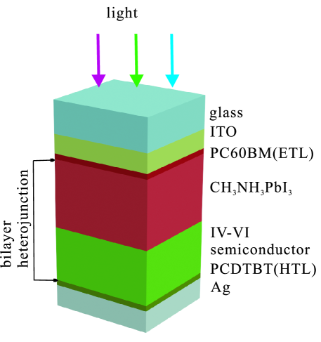
The structure of the bilayer solar cell we propose here is shown in Fig. 1. The top layer is a glass with thickness 100 nm, and the second layer is 80 nm thick Indium tin oxide (ITO) which is taken as the anode of the solar cell. Perovskite (CH3NH3PbI3) layer and IV-VI group semiconductor layer constitute a n-p heterojunction and are taken as active layers expected to absorb almost all light through the whole cell device. As CH3NH3PbI3 as a semiconductor with wide band gap absorbs relatively short wavelength visible light, the layer of narrow-band-gap IV-VI group layered semiconductors under the CH3NH3PbI3 layer can absorb the infrared light. The thickness of CH3NH3PbI3 is taken to be 350 nm according to a previous experiment Lin , and that of the IV-VI group semiconductor layer is set as 450 nm. On the top of CH3NH3PbI3, there is an electronic transport layer (ETL): PC60BM (((6,6)-phenyl-C61-butyric acid methyl ester), and under the IV-VI group semiconductor layer, there is a hole transport layer (HTL): PCDTBT (poly(N-9′-heptadecanyl-2,7-carbazole-alt- 5,5-(4′,7′-di(thien-2-yl)-2′,1′, 3′-benzothiadiazole))) Lin . The bottom layer is 100nm thick Ag as cathode.
For IV-VI group semiconductor layers, here we consider GeSe, SnSe, GeS and SnSe due to their suitable direct bandgaps. The dielectric constants of these materials are taken from Ref. Eymard, . According to the following equation
| (1) |
we can get the refractive index of materials Fox , where and are the real and the imaginary part of dielectric constants, respectively, and and are the real and imaginary part of the refractive index. Taking the refractive index as an input parameter, we use the methods described in Refs. wangDL2014, ; wangDL2015, ; Wang, to calculate the absorption efficiency. The other parameters are taken from Ref. Wang, .
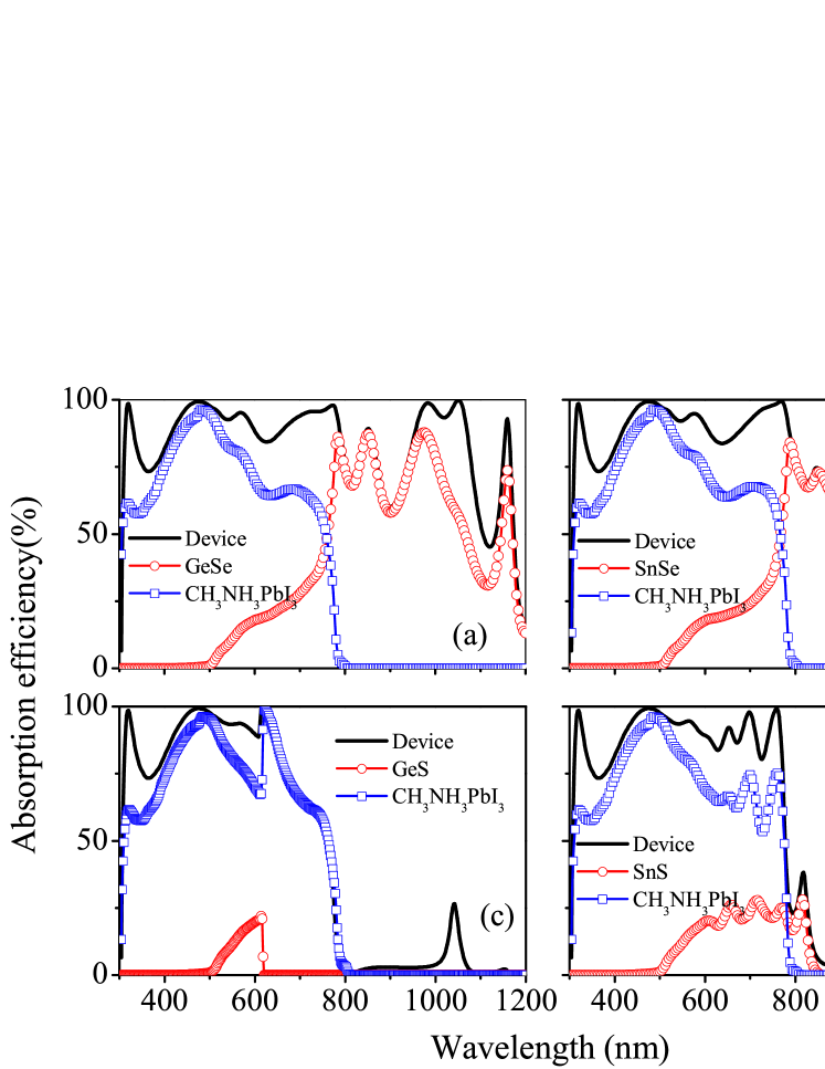
| Materials | GeSe | SnSe | GeS | SnS |
|---|---|---|---|---|
| Bandgap (eV) | 1.1 Elkorashy | 1.047 parenteau | 1.61 Ii | 1.296 parenteau |
| Cutoff wavelength (nm) | 1088 | 1184 | 770 | 957 |
We summarize the experimental bandgaps and corresponding cutoff wavelengths for bulk IV-VI group layered semiconductors, namely GeS, SnS, GeSe, and SnSe in Table 1. As the cutoff wavelengths in the range of nm are proper, GeSe and SnSe may be better choices for the present purpose. This can be seen clearly in Fig. 2 in which the absorption of the solar cell is calculated. “Device” labels the entire absorption for the solar cell consisting of the bilayer heterojunction of CH3NH3PbI3/IV-VI group semiconductor layers. The curves labeled by “CH3NH3PbI3” or IV-VI group semiconductors represent the contributions of these two materials in the cell device. Fig. 2(a) gives the absorption efficiency in the case of GeSe and CH3NH3PbI3 as active layers. One may see that CH3NH3PbI3 shows a strong absorption in the range of 300 nm to 800 nm in accordance with the bandgap. However, there is no absorption when the wavelength is larger than nm. On the contrary, GeSe layer starts to absorb light from a wavelength of nm and dramatically to a high absorption at around nm. When the wavelength is larger than nm, the absorption decreases considerably. It is clear that the light absorption of the perovskite and GeSe layers are complementary to each other. Because of this property, the entire absorption of the bilayer heterojunction comprised of these two materials is perfect in the range of nm to nm. In other words, the CH3NH3PbI3/GeSe bilayer heterojunction solar cell can have a light absorption much better than the single CH3NH3PbI3 layer solar cell.
Although the idea of heterojucntion solar cell is common and an improvement of absorption efficiency can be generally expected, the difficulty is to look for a proper material. One criterion to look for such a material is that the new material should be a direct semiconductor with proper bandgap. This rules out most semiconductors including Si, GaAs, etc. In this sense, we found GeSe can be an ideal candidate for such a purpose. It is noted that GeSe serving as an active layer in the application of single layer solar cells has been tested very recently.
Figs. 2(b)-(d) show the absorption efficiencies of the bilayer heterojunction solar cells with perovskite and SnSe, GeS and SnS, respectively. It is seen that SnSe has also a good absorption in the range of 800 nm to 1200 nm. In comparison to GeSe, although they belong to the same category of materials, GeS and SnS do not show much improvements in absorption as compared with the two selenides. We therefore conclude that GeSe may be the best materials for our bilayer heterojunction solar cell. In the following we shall focus only on GeSe.
III electrical properties and efficiency of the bilayer solar cell
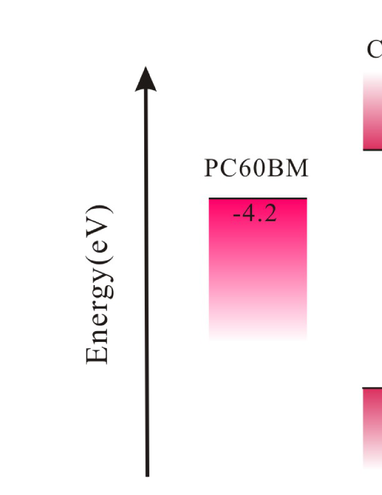
The solar cell must satisfy electron transfer condition, so the work functions of every layer need to be suitable. For this purpose, in Fig. 3, we show the ionization potentials (IPs) of PC60BM and PCDTBT, as well as conduction band and valence band of CH3NH3PbI3 and GeSe. PC60BM and PCDTBT are commonly taken as ETL and HTL, respectively Lin ; Ziaur . ETL and HTL are thin n- or p-type inserted layers between cathode or anode and active layers, which can assist carrier extraction efficiently by reducing the eletrode-junction potential barrier. The IP of PC60BM (-4.2eV) is lower than the conduction band edge of CH3NH3PbI3 (-3.9 eV). Therefore it is easy for electrons to transfer from CH3NH3PbI3 to PC60BM, but it is a barrier for holes. On the other hand, although the valence band edge of GeSe (-5.1eV) is slightly higher than the IP of PCDTBT (-5.3eV), such a small mismatch has little effect on hole transportation.
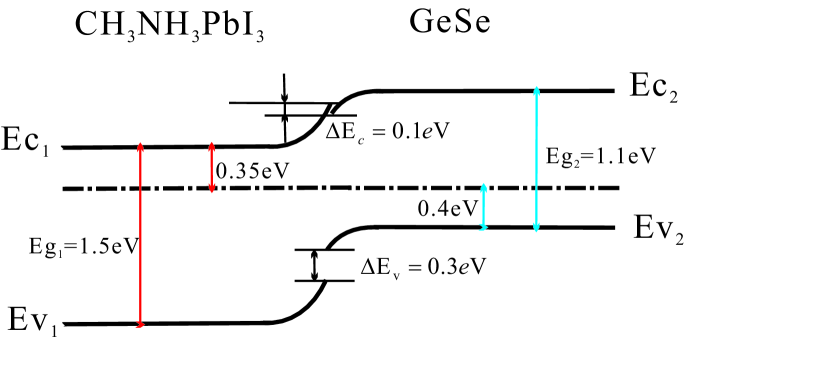
The bilayer heterojunction of perovskite (CH3NH3PbI3) and GeSe can lead to dissociation of electron-hole pairs in the solar cell. The equilibrium band profile of heterojunction is shown in Fig. 4. The position of Fermi level is determined by the relationship between doping concentration and the Fermi energy. When the heterojunction occurs between these two semiconductors, there would be a conduction band step and valence band step . The value of and are given by Milnes
| (2) |
where () is the electron affinity of CH3NH3PbI3 (GeSe), and () is the bandgap of CH3NH3PbI3 (GeSe). The p-type GeSe and n-type CH3NH3PbI3 have the same Fermi level and a small barrier 0.1 eV due to the offset of the conduction band edges. This barrier acts like a Shocttly barrier. However, the effect on photocurrent collection is negligible for a barrier lower than 0.4 eV Nelson . Likewise, there is a small step in the valence band (0.3 eV) which may facilitate the hole transport from CH3NH3PbI3 to GeSe.
Although the optical properties already give some hints, it is still necessary to study the electrical properties for a better conversion efficiency. The electrical properties of a solar cell can be reflected by the short circuit current density, open circuit voltage, fill factor and conversion efficiency. To obtain these quantities, we should first calculate the generation and recombination rates of carriers in the solar cell.
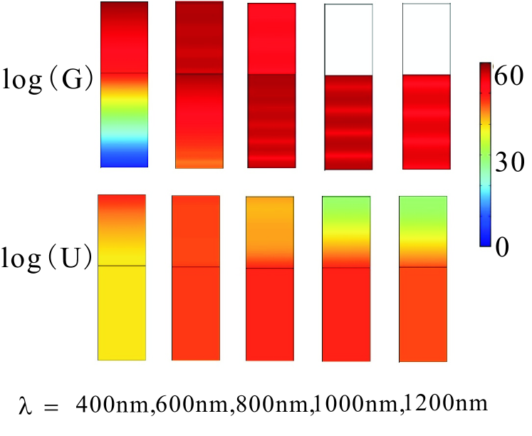
We suppose all the absorbed photons can create excess carriers in the solar cell. The generation rate (G) can be given by an optical simulation. Recombination of carriers is the loss of an electron or hole through the decay to a lower energy state Nelson . Recombination rate (U) can be obtained by an electrical simulation. The details of G and U calculations can be found in Sec. IV. Fig. 5 shows the spatial profiles of G and U when the incident light wavelength is , , , and nm, respectively. The top indicates CH3NH3PbI3 and the bottom represents GeSe, as in Fig. 5. In the top layer (perovskite), G is large for short wavelength (say and nm) of incident light, corresponding to a wider bandgap, and it gradually decreases as the wavelength of incident light increases ( nm). When is larger than nm, the energy of incident light cannot excite excess carriers so that G in the perovskite layer tends to vanish. For the GeSe layer, things go different. For nm, as the energy of incident light is larger than the bandgap of GeSe, G is not zero. However, it may excite the transition to higher bands, and reduce the generation magnitude. For longer , G in GeSe layer increases. When nm, GeSe plays a major role in the device absorption. It is consistent with the optical absorption shown in Fig 2(a). The generation profile shows clearly that the two materials play complementary roles in light absorption of the bilayer cell structure, probably leading to a higher efficiency. The recombination rate U behaves in a way similar to the generation rate G, as the recombination rate is proportional to the excess carriers generated by the incident light.
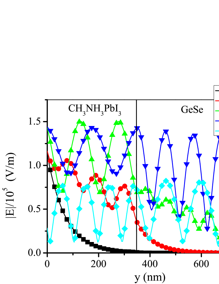
In addition, we observe that G has weak periodic fluctuations in each layer, where the periods of fluctuation depend on . To understand this periodicity, we look at the formula (see Eq. (6) in Sec. IV), where is the imaginary part of permittivity of materials, and is the magnitude of electric field. The oscillation of the generation rate G is due to the oscillation of electric field. We show the spatial dependence of in Fig. 6. For nm, the electric field decays exponentially from perovskite layer to GeSe layer. For nm, the electric field oscillates in perovskite layer, while it decays in GeSe layer. For longer wavelengths ( nm), the electric field oscillates all over the bilayer. This oscillation of the magnitude of electric field reflects perfectly the periodicity of the generation rate G. With the increase of wavelength, the penetration depth of light increases so that more light can arrive at a deeper position, even reaching the bottom Ag layer where the light can be reflected then. The vanishing generation rate G in perovskite layer for nm is not a consequence of , but a vanishing for a long wavelength (with corresponding energies less than the bandgap of perovskite).
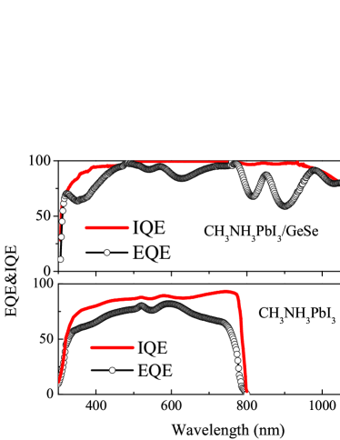
We solve the Poisson’s equation and carrier transport equations self-consistently X Li , and obtain the internal quantum efficienc (IQE) and external quantum efficiency (EQE), as shown in Fig. 7(a). For a comparison, we also calculate EQE and IQE of the single layer perovskite solar cell [Fig. 7(b)]. It can be seen that the EQE and IQE of perovskite/GeSe bilayer solar cell distribute in the range of nm to nm of the solar spectra, while those of the single layer perovskite cell only distribute in the range of nm.
The resistance of solar cells is important in evaluating the efficiency, which, however, is difficult to calculate via a microscopic theory due to complicated scattering mechanisms. Fortunately, an equivalent circuit for a solar cell always contains the parasitic series () and shunt () resistance. The shunt resistance is caused by the leakage current of the device generally due to the non-ideal devices Nelson . The series resistivity has two main sources. One is from the contact resistances due to multi-interfaces between heterojunction, the active layer and the contacts, etc. The other is from the drift current density neamen , i.e. , where is the mobility of electrons (holes), is the electron (hole) concentration, and is the conductivity of the semiconductor material. It leads us to the drift resistivity
| (3) |
In a doped material, the drift resistivity is dominated by the majority carrier concentration and mobility. The drift resistance is therefore determined by the drift resistivity multiplying the material thickness. In terms of the parameters listed in Table 3, we obtain the drift resistance of GeSe (CH3NH3PbI3) as cm2 ( cm2). For the contact resistance, it is hard to know the value precisely. The total series resistance should be a sum of the total drift resistance and the contact resistance in the device. Since the contact resistivity is hard to obtain precisely, we assume that the series resistances of GeSe layer and perovskite layer are the same and equal to that of a single perovskite layer studied in Ref. Wang, in which the perovskite solar cell is explored and its resistance is cm2. In this way, the total series resistance of the bilayer solar cell is cm2. The shunt resistance of the bilayer cell is assumed to be the same as that of a perovskite solar cell in Ref. Wang, , which is 1.6 cm2.
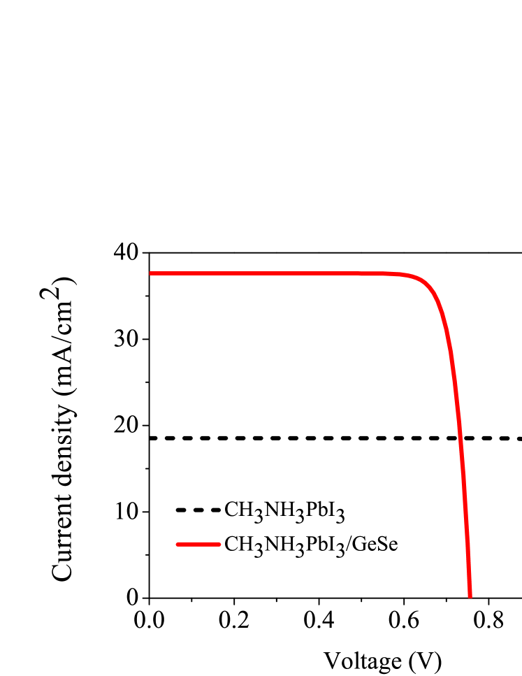
Through the electrical simulation, curve for the bilayer solar cell is presented in Fig. 8. For a comparison, we include the curve for typical perovskite solar cell as well. We also obtain the short circuit current density (), the open circuit voltage (), the fill factor () and the conversion efficiency, as shown in Table 2. Compared with the conventional perovskite solar cell, the is improved significantly in the present bilayer solar cell, which is supported by the values of mA/cm2 for the bilayer solar cell and 18.53 mA/cm2 for the single-layer solar cell. This rise of stems from more absorption of long wavelength light by introducing GeSe layer in the solar cell. The of the bilayer solar cell is V, which is smaller than V of the typical perovskite solar cell. The of bilayer solar cell is slightly smaller than that of the perovskite solar cell since GeSe layer leads to a larger series resistance. By combining these parameters together, we obtain the efficiency of the perovskite/GeSe bilayer solar cell to be 23.77%, which is much higher than 16.66 % of the conventional perovskite solar cell. The main reason for such a dramatic improvement is from a big increase of the short circuit current density. This observation demonstrates that our strategy of improving the output energy density in a single solar cell is reasonable. This may pave a way to improve the conversion efficiency further.
Here we would like to remark that, recently, the efficiency of conventional perovskite solar cell has been much improved in experiments, which can be over e.g. singlePerovskitesolarcell . In practice, a 350 nm thick perovskite layer might not be sufficient for planar solar cells ZLiu . However, in our study, we aim to demonstrate the applicability of the perovskite/GeSe bilayer solar cell, and fix the thickness of perovskite layer to be 350 nm, leading to the calculated efficiency () of the perovskite solar cell is lower than those reported very recently singlePerovskitesolarcell . If the thickness of the perovskite is increased, the efficiency should be further enhanced.
We have some remarks here. Firstly, the hetero-junction structure may bring us more complexities. Extra defects may be introduced around the interface, which could increase the recombination rate and reduce the open circuit voltage. Therefore, they should be minimized in realistic applications. This might be achieved at some extent by using advanced nanotechnologies that may lead us atomic-resolved ideal interfaces. For the possible defects of dangling bonds, an inter-layer may be added to passivate them. Secondly, the crystal mismatch should be also considered. In our case, the crystal constants of the c-axis of perovskite and of the a-axis of GeSe are ÅMosconi and ÅMakinistian respectively. The mismatch of the crystal constants is 14.2% from and not so large. Moreover, in realistic applications, inserting buffer layers may be an alternative way to soften the mismatch. Thirdly, the carrier separation in the internal of each layer should be taken into account as well. For single p-n junction solar cells, the illumination of light can generate electron-hole pairs, which can be separated and swept out to produce the photocurrent due to the built-in electric field in the depletion region neamen . Therefore, the thickness of the depletion region is quite important for a single p-n junction solar cell. In the present case, the calculated depletion lengths in GeSe and perovskite are about m and nm, and the thicknesses of the GeSe layer and the perovskite layer are nm and nm, respectively. We may state that the separation mechanism in the depletion region can work well in our device.
| Device type | (mA/cm2) | (V) | () | Efficiency() |
|---|---|---|---|---|
| perovskite/GeSe | 37.62 | 0.76 | 83.14 | 23.77 |
| perovskite | 18.53 | 1.02 | 88.15 | 16.66 |
| Properties | GeSe | CH3NH3PbI3 |
|---|---|---|
| doping (cm-3) | 3.54 | 9.83 |
| bandgap (eV) | 1.14 | 1.5 |
| electron mobility (m) | 0.05 | 1 |
| hole mobility (m) | 0.05 | |
| electron effective mass () | 0.3 | 2 |
| hole effective mass () | 0.78 | 0.6 |
| electron lifetime () | 0.01 | 9.6 |
| hole lifetime () | 0.01 | 9.6 |
| relative permittivity | 6.3 | 25 |
IV Methods
Optical properties can be obtained by solving Maxwell equations in a finite element method (FEM) software package Li . We consider both the transverse electric (TE) and transverse magnetic (TM) polarized incident light and take the average of these two modes. The AM1.5 global spectrum is used as incident solar spectrum in optical simulation. Refractive index and extinction coefficient of materials are input parameters of all layers in a solar cell and then the optical absorption efficiency of the device can be obtained by
| (4) |
where is the distribution of the electric field intensity in each layer of solar cell as a function of wavelength, is the angular frequency of incident light, is the imaginary part of permittivity of materials, is the integral unit for volume of the solar cell. The density of photo-generated current () is given by Yu
| (5) |
where is the charge of an electron, is the speed of light, is the Planck constant, is the spectral photon flux density in solar spectrum (AM 1.5). Light absorption leads to the generation of excess carriers with a generation rate expressed by
| (6) |
were is the reduced Planck constant. The electrons in excited states can relax to unoccupied states with lower energies at a recombination rate given by
| (7) |
where is the intrinsic carrier concentration of semiconductor, and are lifetimes of electrons and holes, respectively, () is electron (hole) concentration in a trapped energy level. The electrical properties of solar cell is accomplished by solving Poisson’s equation and carrier transport equations Ferry ; Deceglie . The electrostatic potential () is determined by Poisson’s equation, and electron and hole concentrations can be obtained by
| (8) |
where is the doping concentration, and are the vacuum and relative permittivity, respectively, is the electron (hole) diffusion coefficient. Moreover, it is important to choose suitable initial values of parameters in the simulation as input. The initial potential is set by X Li
| (9) |
where is the Boltzmann constant, and is temperature. The initial carrier concentrations are set by
| (10) |
The parameters used in this device are presented in Table 3, which are taken from Refs. Vodenicharov, ; Elkorashy, ; Wang, ; Xue, .
V Conclusion
To improve the power conversion efficiency of the typical perovskite solar cell, we studied a bilayer solar cell with perovskite CH3NH3PbI3 and IV-VI group semiconductor materials forming a heterojunction. Four semiconductors are considered in this paper, say, GeSe, SnSe, GeS, and SnS. The bandgaps of these four materials are suitable for the absorption of long wavelength light, which might have a complementary contribution to the perovskite that is almost predominant in the visible light. If one replaces the single perovskite layer with a perovskite/IV-VI group semiconductor bilayer in the solar cell, the absorption efficiency of the cell should be improved remarkably. After some efforts, we found that GeSe is the best candidate for such a bilayer solar cell. As a consequence, for CH3NH3PbI3/GeSe bilayer structure, the short circuit current density is dramatically improved, leading to the power conversion efficiency is promoted to , being larger than that of the conventional perovskite solar cell within the same calculation. This present study may shed new light on developing perovskite solar cells with high efficiency and good performance.
VI Acknowledgment
We gratefully thank Qing-Rong Zheng, Qing-Bo Yan and Zheng-Chuan Wang for instructive discussions. This work is supported by Hundred Talents Program of The Chinese Academy of Sciences and the NSFC (Grant No. 11674317). G. S. is supported in part by the MOST (Grant No. 2013CB933401), the NSFC (Grant No. 11474279) and the CAS (Grant No.XDB07010100).
References
- (1) J. P. Reithmaier, P. Paunovic, W. Kulisch, C. Popov, and P. Petkov, Nanotechnological Basis for Advanced Sensors, (Springer, New York, 2011).
- (2) S. Moon, K. Kim, Y. Kim, J. Heo, and J. Lee, Sci. Rep. 6, 30107 (2016).
- (3) N. Asim, K. Sopian, S. Ahmadi, K. Saeedfaret, M. A. Alghoul, O. Saadatian, and S. H. Zaidi, Renewable and Sustainable Energy Reviews. 16, 5834 (2012).
- (4) A. Shah, P. Torres, R. Tscharner, N. Wyrsch, and H. Keppner, Science. 285, 692 (1999).
- (5) J. -M. Nunzi, Comptes Rendus Physique 3, 523 (2002).
- (6) H. Hoppe, N. S. Sariciftci, J. Mater. Res. 19, 1924 (2004).
- (7) J. Zhao, Y. Li, G. Yang, K. Jiang, H. Lin, H. Ade, W. Ma, and H. Yan, Nat. Energy. 1, 15027 (2016).
- (8) Q. Lin, A. Armin, R. C. R. Nagiri, P. L. Burn, and P. Meredith, Nat. Photonics. 9, 106 (2015).
- (9) X. Li, D. Bi, C. Yi, J. Decoppet, J. Luo, S. M. Zakeeruddin, A. Hagfeldt, and M. Gratzel, Science. 353, 58 (2016).
- (10) C. Zuo, H. J. Bolink, H. Han, J. Huang, D. Cahen, and L. Ding, Adv. Sci. 3, 1500324 (2016).
- (11) F. Fu, T. Feurer, T. Jager, E. Avancini, B. Bissig, S. Yoon, S. Buecheler, and A. N. Tiwari, Nat. Commun. 6, 8932 (2015).
- (12) M. A. Green, A. Ho-Baillie, H. J. Snaith, Nat. Photonics 8, 506 (2014); W. -J. Yin, T. Shi, Y. Yan, Adv. Mater. 26, 4653 (2014).
- (13) M. Santamouris, Advances in Passive Cooling, (Earthscan, London, 2008).
- (14) S. P. Bremner, M. Y. Levy, and C. B. Honsberg, Prog. Photovolt: Res. Appl. 16, 225 (2008).
- (15) D. D. Vaughn II, R. J. Patel, M. A. Hickner, and R. E. Schaak, J. Am. Chem. Soc., 132, 15170 (2015).
- (16) K. F. A. El-Rahmana, A. A. A. Darwishb, and E. A. A. El-Shazlya, Mat. Sci. Semicon. Proc. 25, 123 (2014).
- (17) Z. Deng, D Cao, J. He, S. Lin, S. M. Lindsay, and Y. Liu, Acs Nano. 6, 6197 (2012).
- (18) L. Huang, F. Wu, and J. Li, J. Chem. Phys. 144, 114708 (2016).
- (19) R. K. Ulaganathan, Y. Y. Lu, C. J. Kuo, S. R. Tamalampudi, R. Sankar, K. M. Boopathi, A. Anand, K. Yadav, R. J. Mathew, C. R. Liu, F. C. Chou, and Y. T. Chen, Nanoscale. 8, 2284 (2016).
- (20) A. M. Elkorashy, phys. stat. sol. 152, 249 (1989).
- (21) G. Shi and E. Kioupakis, Nano Lett. 15, 6926 (2015).
- (22) R. Eymard and A. Otto, Phys. Rev. B. 16, 1616 (1977).
- (23) M. Fox, Optical Properties of Solids, (Oxford University Press, Oxford, 2001).
- (24) D. L. Wang, H. J. Cui, G. J. Hou, Z. G. Zhu, Q. B. Yan and G. Su, Sci. Rep. 6, 18922 (2016).
- (25) D. L. Wang and G. Su, Sci. Rep. 4, 7165 (2014).
- (26) D. L. Wang, H. J. Cui, and G. Su, Solar Energy 120, 505 (2015).
- (27) R. S. Ziaur, M. Siddheswar, D. Atanu, P. Amit, Y. H. Wu, C. S. Lai, T. C. Tien, W. S. Chen, H. Y. Lee, F. T Chen, M. J. Tsai, and L. B. Chang, Nanoscale Res. Lett. 7, 614 (2012).
- (28) A. G. Milnes and D. L. Feucht, Heterojunctions and Metal-Semiconductor Junctions, (Academic, New York 1972).
- (29) J. Nelson, The Physics of Solar Cell, (Imperial College Press, London, 2002).
- (30) X. Li, N. P. Hylton, V. Giannini, K. H. Lee, N. J. Ekins-Daukes, and S. A. Maier, Photovolt: Res. Appl. 21, 109 (2013).
- (31) D. A. Neamen, Semiconductor Physics and Devices: Basic Principles, (McGraw-Hill, New York, 2003).
- (32) S. S. Shin,E. J. Yeom, W. S. Yang, S. Hur, M. G. Kim, J. Im, J. Seo, J. H. Noh, S. I. Seok, Science 356, 167 (2017); D. -Y. Son, J. -W. Lee, Y. J. Choi, I. -H. Jang, S. Lee, P. J. Yoo, H. Shin, N. Ahn, M. Choi, D. Kim, and N. -G. Park, Nat. Energy 1, 1 (2016).
- (33) Z. Liu, J. Hu, H. Jiao, L. Li, G. Zheng, Y. Chen, Y. Huang, Q. Zhang, C. Shen, Q. Chen, and H. Zhou, Adv. Mater. 29, 1606774 (2017).
- (34) E. Mosconi, A. Amat, M. K. Nazeeruddin, M. Grätzel, and F. D. Angelis, J. Phys. Chem. C. 117, 13902 (2013).
- (35) L. Makinistian and E. A. Albanesi, J. Phys.: Condens. Matter. 19, 186211 (2007).
- (36) Y. Yu, V. E. Ferry, A. P. Alivisatos, and L. Cao, Nano Lett. 12, 3674 (2012).
- (37) M. G. Deceglie, V. E. Ferry, A. P. Alivisatos, and H. A. Atwater, Nano Lett. 12, 2894 (2012).
- (38) V. E. Ferry, A. Polman, and H. A. Atwater, ACS Nano. 5, 10055 (2011).
- (39) C. Vodenicharov and S. Parvanov, Mater. Chem. Phys. 21, 455 (1989).
- (40) D.J. Xue, S. C. Liu, C. M. Dai, S. Chen, C. He, L. Zhao, J. Hu, and L. J. Wan, J. Am. Chem. Soc., 139, 958 (2017).
- (41) M. Parenteau, and C. Carlone, Phys. Rev. B, 41, 5227 (1990).