Mobility gap and quantum transport in functionalized graphene bilayer
Abstract
In a Bernal graphene bilayer, carbon atoms belong to two inequivalent sublattices A and B, with atoms that are coupled to the other layer by bonds belonging to sublattice A and the other atoms belonging to sublattice B. We analyze the density of states and the conductivity of Bernal graphene bilayers when atoms of sublattice A or B only are randomly functionalized. We find that for a selective functionalization on sublattice B only, a mobility gap of the order of eV is formed close to the Dirac energy at concentration of adatoms . In addition, at some other energies conductivity presents anomalous behaviors. We show that these properties are related to the bipartite structure of the graphene layer.
-
March 2018
Keywords: Graphene bilayer, functionalization, quantum transport
1 Introduction
Electronic properties at nanoscale are the key to the novel applications of low-dimensional and nanomaterials in electronic and energy technologies. In particular, a lot of research has been devoted to understanding the remarkable electronic structure and transport properties of bilayer (or multilayers) of graphene [1, 2, 3, 4, 5, 6, 7, 8, 9, 10, 11, 12, 13, 14]. Depending on the stacking, the charge carriers were shown, both theoretically [15, 16, 17, 18, 19, 20, 21] and experimentally [22, 23, 24, 25, 26, 27], to behave like massless Dirac particles or massive particles with chirality. Electronic properties can be tuned by various means and in particular by electrostatic gate or by adding of static defects and functionalization by adatoms or admolecules of monolayer (MLG) [7, 28, 29, 30, 31, 32, 33, 34, 35, 36, 37, 38, 39, 40, 13, 14, 41, 42] and bilayer (BLG) [26, 24, 20, 21]. For example, one can open a band gap in this system by electrostatic gating [22, 23]. Recently such locally coupled structures have been also observed in chemical vapor deposition (CVD) graphene samples [26, 41] where, due to rippling, the layers were decoupled in some regions, while being connected in others. It has also been shown that UV irradiation, which results in water dissociative adsoption on graphene of few % of adsorbates, can induce a tunable reversible gap [42].
In this work, we investigate the density of states and the conductivity of a Bernal bilayer graphene (BLG) when the upper layer is functionalized by adatoms. There are two types of site on the upper layer, as shown in Figure 1. Sites of sublattice A are above a carbon atom of the lower layer whereas sites of sublattice B are not. Therefore it is possible in principle to functionalize selectively atoms which belong to sublattice A or to sublattice B only. We consider here, that, within the functionalized sublattice, the repartition of the functionalized atoms is random. As a main result we find that, when only sublattice B is functionalized a mobility gap of the order of eV is formed close to the Dirac energy at concentration of adatoms . Furthermore for both sublattice functionalization the conductivity increases in some Fermi energy window, when the concentration of functionalized sites increases. This is because the functionalization is not just introducing scattering centers but deeply changes the electronic structure. As we show the creation of the gap and the abnormal behavior of the conductivity are related to the bipartite nature of the monolayer and bilayer graphene.
2 Method
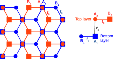
The BLG studied here consist of the bottom layer 1 and of the top layer 2 as shown in Figure 1. The top layer 2 is functionalized whereas the bottom layer 1 keeps its perfect structure. There are four carbon atoms in the unit cell, two carbons A1, B1 in layer 1 and A2, B2 in layer 2 where A2 lies on the top of A1. We use an electronic model where only orbitals are taken into account, since we are interested in the low energy physics i.e. electronic states close to the Dirac energy. The adsorbates which create a covalent bond with a carbon atom of the graphene upper layer is represented by removing the orbitals of the functionalized carbon atoms [43, 44, 7, 45, 31, 46]. The missing orbitals are distributed randomly only on sites of the top layer 2 in the sublattice A or B. The tight-binding (TB) Hamiltonian for orbitals has the form:
| (1) |
where and create and annihilate respectively an electron on site , is the sum on index and with , and is the hopping matrix element between two orbitals and . We analyze the average local density of states (LDOS) on the sublattices A or B of each plane, and the conductivity as a function of the position of the Fermi energy. Densities of states are computed by recursion (Lanczos algorithm) [47] in real-space on sample containing a few carbon atoms with periodic boundary conditions. Within the Kubo-Greenwood formalism we compute the microscopic conductivity [37] using the real-space method developped by Mayou, Khanna, Roche and Triozon [48, 49, 50, 51, 52] (see supplementary material [53] Sect. 4). is the semi-classical conductivity that does not take into account the quantum corrections due to multiple scattering effects. Typically this quantity represents a room temperature conductivity when multiple scattering effects are destroyed by dephasing due to the electron-phonon scattering.
3 Results
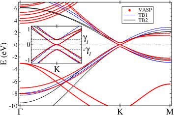
We present first calculations performed with the standard nearest neighbor hopping Hamiltonian (TB1): eV for intra-layer hopping between A and B atoms, and eV for nearest neighbor inter-layer hopping between A1 and A2 atoms. The advantage of this simple Hamiltonian TB1 is to allow a detailed physical discussion of the physical mechanism involved. These results are confirmed by analyzing a more realistic Hamiltonian description that takes into account hopping beyond the nearest neighbor hopping model (TB2) (supplementary material [53], Sect. 1). TB2 has been used successfully to study the electronic structure in rotated bilayer of graphene [17, 18, 19] in good agreement with STM density of states measurements [54, 55] and for transport calculations [35, 37, 38, 21].
3.1 Results with nearest-neighbor hopping Hamiltonian (TB1)
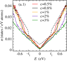
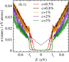


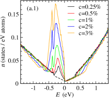
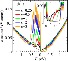
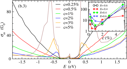
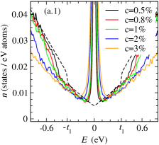
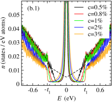
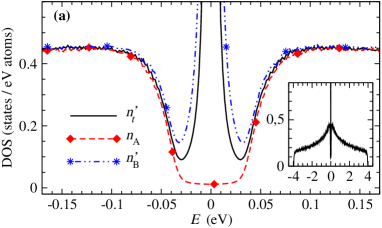
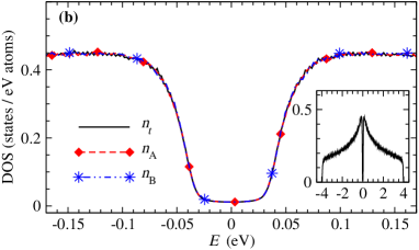
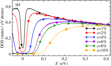
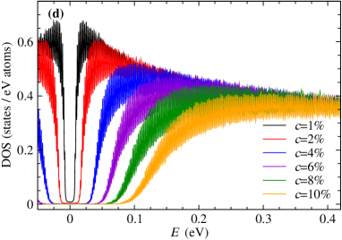
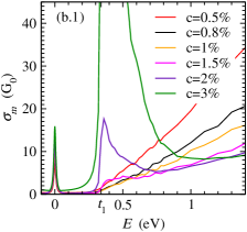
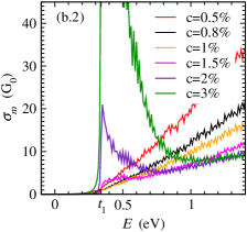
The total density of states for both layers (TDOS), , are shown figures 2(a.1) and 2(b.1) respectively for A and B vacant atoms in layer 2. As explained in the following and in supplementary material [53] (Sect. 2), each missing orbital in the A2 sublattice (resp. B2 sublattice) of the top layer 2 produces one midgap states at Dirac energy that spreads on {A1, B2} sublattices (resp. {A2, B1}). This is similar to the case of a monolayer of graphene where vacancies in sublattice A (resp. B) produce midgap states at Dirac energies that are located in sublattice B (resp. A) [56, 44]. In figures 2(a.1), 2(b.1) and 2(c) the midgap states at are not included in plotted DOSs and in the calculation of the conductivity (supplementary material [53] Sect. 2 and 4). Vacancies on the A2 sublattice do not produce a gap in the TDOS, whereas B2 vacancies induce a quasi-gap clearly seen around . Its width, , increases when increases and saturates at a value . In B2 vacancies case, unphysical small oscillations appeared in the total DOS and local DOSs. Those oscillations are numerical artifacts related to the termination of the continuous fraction expansion of the Green function used in the recursion method (see supplementary material [53] Sect. 2, 3, and Ref. [47]). The presence of these unphysical oscillations in the case of B2 vacancies whereas there is no oscillations in the cases of A1 vacancies, confirms the emergence of a gap by B2 vacancies.
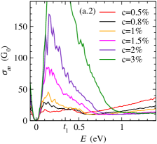
The conductivity , is shown figures 2(a.2) and 2(b.2) for A2 vacant atoms and B2 vacant atoms, respectively. In both cases, the conductivity at large energies eV is inversely proportional to the concentration of vacancies. This is expected from the Boltzmann theory if the vacancies are seen only as scattering centers which give a finite lifetime to the eigenstates of the perfect Bernal bilayer. For smaller energies, corresponding to usual values, the variation of the conductivity with the concentration of vacancies is not consistent with Boltzmann theory. Indeed, with vacancies on A2 sublattice, for small values, increases strongly when increases. With vacancies on B2 sublattice, for energies above the quasi-gap, i.e. , if %, decreases when increasses (as expected in Boltzmann theory); whereas for , increases when increases.
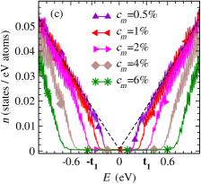
All these spectacular results show that the effect of selective functionalization is not just to induce scattering for the states of the perfect bilayer. This is also confirmed by analyzing the selective functionalization of a sublattice of the MLG. As shown in figure 2(c), it leads to the creation of a quasi-gap which width increases with concentration of adatoms. Let us recall that for a monolayer and bilayer with vacancies that are randomly distributed on the two sublattices A and B (Refs. [46, 57, 37, 21] and Refs. there in) the low energy DOS presents a peak which is reminiscent of the midgap states but has a finite width.
3.2 Results with Hamiltonian including hopping beyond nearest neighbor (TB2)
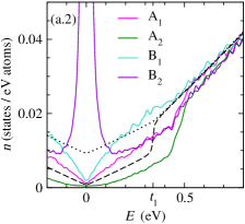
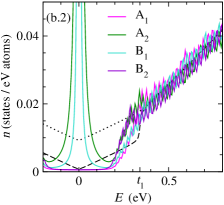
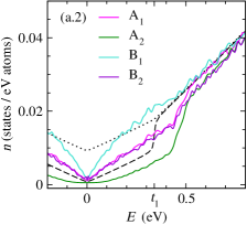
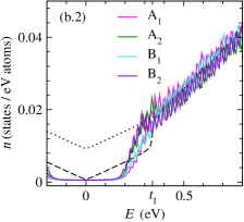
Now we present results calculated using TB2 model, including hopping beyond nearest neighbors, in place of TB1 model (supplementary material [53] (Sect. 1)). The TDOS, , the average LDOS, with A1, A2, B1, B2, and the conductivity, , are shown in figures 3 for A2 vacant atoms and B2 vacant atoms. In both cases the midgap states, produced by missing orbitals are displaced to negative energy by the effect of the hopping beyond nearest neighbors (TB2) as in MLG [44, 35, 38] and BLG with vacancies randomly distributed [21]. In addition these states appear in an energy window of a fraction of an eV that depends on the concentration of functionalized sites. It is interesting to note that the peak of vacancy states is split into a double peak when we increase the concentration of vacancies. That splitting indicates a coupling between vacancy states that are all located on the same sublattice. The symmetry of the electronic properties with respect to of TB1 model is broken; but, qualitatively, the anomalous conductivity found in the case of TB1 model is still found with TB2 model. The main difference between TB1 and TB2 is in the energy window where the midgap states appear.
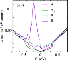
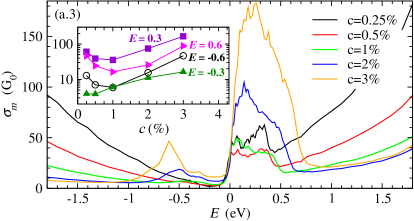
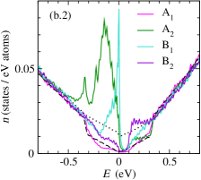
With A2 vacant atoms, the average LDOS (figure 3(a.2)) shows that midgap states is located on orbitals of the same layer, as expected from the uncompensated theorem with TB1. For %, increases strongly when increasses (figure 3(a.3)). This increase is maximum (several order of magnitude) for energies close to and eV, and it is smaller for energies corresponding to the midgap peak.
With B2 vacant atoms, the average LDOS (figure 3(b.2)) shows that midgap states is located on orbitals (layer 2) and on orbitals (layer 1), as expected from a bipartite Hamiltonian analysis with TB1 [58]. The quasi-gap is found for , instead of with TB1, since for negative energies midgap states are present in the case of TB2. is very small for corresponding to midgap states, and theses energies correspond at a mobility quasi-gap (figure 3(b.3)). As a result, similarly to TB1 model, a mobility quasi-gap is found for with TB2 too. Moreover for –% and for , increases strongly when increases (as with TB1).
4 Discussion: Interpretation of the results by bipartite lattice.
We analyze now the origin for the formation of the gap in the MLG with selective functionalization on sublattice A (or B) and then show how it leads to the properties of the BLG. Quite generally an eigenstate with energy of the MLG with or without vacancies, can be writen as , with states () belonging to the sublattice (). It is easy to show that and are eigenstates of the effective Hamiltonian with eigenvalue . acts only within the sublattices and and does not couple them.
For example for the perfect MLG, is the Hamiltonian of a triangular lattice of A atoms (B atoms),
| (2) |
where and creates and annihilates respectively a state of an electron , and with and . The middle of band () corresponds to the lowest energy of band ().
The effect of vacancies on the DOS away from zero energy can be understood by considering the effective Hamiltonian of the sublattice that contains the vacancies. This Hamiltonian has the form given in equation (2) but with functionalized sites that are simply deleted. Without vacancies the coordination of each atoms of A sublattice is 6. With a small concentration of vacancies in A sublattice, the average coordination is . The center of the A band is fixed by on-site energies, , and it is not affected by vacancies; but the width of the band will decrease when decreases (i.e. when increases). As expected from this simple tight-binding argument, the minimum values, , of the spectrum of , found numerically (figure 2(d)), is almost proportional to the average coordination number (average number of A–A (B–B) nearest neighbors of A (B) sublattice of the bipartite lattice). Consequently the average A DOS, , has a gap induced by vacancies for . This means that DOS in the A and B sublattices of MLG also presents a gap for (figure 2(c)) As is well known each vacancy in sublattice also induces a zero energy midgap states in sublattice . Note that similar results are obtained on a square lattice which is also a bipartite lattice (supplementary material [53], Sect. 3).
Let us consider now the case of the bilayer with vacancies on the A2 sublattice. In this case the midgap states of the top layer 2 are located only on sublattice B2 and are not coupled to the lower layer 1. Therefore layer 1 is just coupled to a semi-conductor (top layer 2) with a gap in the energy range . The results shown above mean that is sufficiently small that the mixing between states of layer 1 and 2 is small. Therefore layer 1 has essentially the electronic structure of an isolated MLG without defects. This explains why the TDOS is similar to that of a graphene layer. In addition when the vacancies concentration increases, increases and the decoupling between the two layers is more efficient. Therefore at a given energy the lifetime of states in the lower layer 1 increases and the conductivity increases when concentration increases. Transport in the bilayer at these energies is mainly through the lower layer 1.
The case of vacancies on the B2 sublattice is slightly more complex. Again at energies such that the mixing between states of layer 1 and states in the continuum of layer 2 is small. However in that case the midgap states of layer 2 are located on sublattice A2 and are coupled to the sublattice A1 of the lower layer 1. The effect of the interlayer coupling alone is to couple midgap states of A2 with specific linear combinations of states of A1 and to produce bonding and anti-bonding states at energies and . We consider now the case where the concentration of adatoms is sufficient to have . Therefore at energies such that these specific states in sublattice A1 appear as decoupled from the other states of layer 1. They act thus as vacancies in the MLG (layer 1) and this produces a quasi-gap with midgap states in sublattice B of layer 1. For that reason, a quasi-gap exists in both layers in the energy range and it is seen in the TDOS. Similarly to the previous case, increasing the concentration can also increase the conductivity for energies such that .
These analyses of the effect of selective functionalization are confirmed by detailed studies of the bipartite Hamiltonian of BLG [58].
5 Conclusion
We have analyzed the density of states and the conductivity of graphene Bernal bilayer (BLG) when the upper layer is functionalized by adatoms. Since there are two inequivalent sublattices A and B, that correspond to carbon atoms that are more or less coupled to the lower layer, we study the effect of a selective functionalization of sublattices A or B. As we show this selective functionalization leads to the creation of a gap when sublattice B of the upper layer is randomly functionalized with a concentration of adatoms . This gap is a fraction of one eV for the DOS and of at least eV for the mobility. This phenomenon is intimately related to the bipartite structure of the graphene lattice and the maximum width of the gap is of the order of the interlayer coupling energy. Other functionalizations of sites are possible if both layers can be functionalized. In this case also we find that electronic structure and transport properties can be deeply modified by a selective functionalization [58]. We believe that the phenomenon due to selective functionalization could be observed in carefully prepared graphene bilayers or even in other 2D materials.
Acknowledgments
The authors wish to thank C. Berger, W. A. de Heer, L. Magaud, P. Mallet and J.-Y. Veuillen for fruitful discussions. The numerical calculations have been performed at Institut Néel, Grenoble, and at the Centre de Calculs (CDC), Université de Cergy-Pontoise. We thank Y. Costes, CDC, for computing assistance. This work was supported by the Tunisian French Cooperation Project (Grant No. CMCU 15G1306) and the project ANR-15-CE24-0017.
Supplementary Material
In this supplementary material, we first (section 1) present the tight-binding models for Bernal bilayer graphene (BLG): TB1 that includes only the first neighbor hoppings, and a more realistic model, TB2, that includes hopping beyond first neighbors. In section 2, we discuss midgap states at energy with the density of states (DOS) of BLG calculated with TB1. Section 3 presents the electronic structure of a bipartite square lattice with vacancies in a sublattice. The method to compute Kubo-Greenwood conductivity is described section 4.
1. Tight-binding Hamiltonian Models
In this part, we present in details the tight-binding (TB) schemes. Bilayer graphene (BLG) consists in four carbon atoms in its unit cell, two carbons A1, B1 in layer 1 and A2, B2 in layer 2 where A2 lies on the top of A1. Only orbitals are taken into account since we are interested in what happens at the Fermi level. The Hamiltonian has the form :
| (3) |
where and create and annihilate respectively an electron on the orbital located at , is the sum on index and with , and is the hopping matrix element between two orbitals located at and . We consider two model Hamiltonians.
The first model (TB1 model) is the simplest TB model with first-neighbor hopping only. Each atom has 3 first neighbors in the same plane with hopping between pz orbitals eV. The inter-layer hopping between pz orbitals between A1 and first neighbor A2 is eV to reproduce similar band dispersion as in ab-initio calculations (figure S1). Inter-layer hopping splits two bands of MLG Dirac cone in two parabolic bands separated by (figure S1). With the TB1 model, eV, the spectrum is symmetric with respect to Dirac energy , .
The second model (TB2 model) is more realistic where hopping terms are not restricted to nearest neighbor hopping. We have used this model Hamiltonian in our previous works [17, 18, 19, 21] to study electronic structure of the rotated graphene bilayers. It reproduces the ab initio calculations of the electronic states for energies within eV of (figure S1). The hopping terms are computed from Slater-Koster parameters,
| (4) |
where is the direction cosine of along axis and is the distance between the orbitals,
| (5) |
is the coordinate of along . is either equal to zero or to a constant because the two graphene layers have been kept flat in our model. We use the same dependence on distance of the Slater-Koster parameters:
| (6) | |||||
| (7) |
where is the nearest neighbor distance within a layer, Å, and is the interlayer distance, Å. First neighbor interaction in a plane is taken equal to the commonly used value, eV [8]. Second neighbor interaction in a plane is set [8] to ; that fixes the value of the ratio in equation (6). The inter-layer hopping between two orbitals in configuration is . is fixed to obtain a good fit with ab-initio calculation around Dirac energy in AA stacking [18] and AB bernal stacking and then to get eV (figure S1) which results in eV. We choose the same coefficient of the exponential decay for and ,
| (8) |
with Å the distance between second neighbors in a plane.
We consider that resonant adsorbates –simple atoms or molecules such as H, OH, CH3– create a covalent bond with some carbon atoms of the BLG. To simulate this covalent bond, we assume that the orbital of the carbon, that is just below the adsorbate, is removed. In our calculations, the mono-vacancies are distributed at random on one sublattice, i.e. on one type of atom in one layer, with a finite concentration .


2. Midgap states in case of first neighbor hopping model (TB1) with vacancies on a sublattice only
The total density of states (total DOS) is computed by recursion (Lanczos algorithm) [47] in real-space on sample containing carbon atoms, is up to a few , with periodic boundary conditions. Considering a random phase states , [50]
| (9) |
where the orbital of atom and is a random number between 0 and 1, the total DOS is
| (10) |
with
| (11) |
The DOS at energy is thus evaluated numerically from a continuous fraction expansion of the Green function, , with and a finite small value [47]. Therefore, the computed DOS is the real DOS convoluted with the Lorentzian function,
| (12) |
of half width . Roughly speaking, is a kind of energy precision of the calculation. As is small, should be large. DOSs presented in this paper are computed with meV.
Average local DOSs, on a sublattice, A1, B1, A2, B2 are obtained using the same numerical method with a random phase expands on the orbitals of the sublattice,
| (13) |
where is the index of atoms of the sublattice that contains atoms. Figure S3 shows total DOS and average local DOSs , calculated with TB1, for BLG with vacancies on A2 and B2 sublattice respectively.
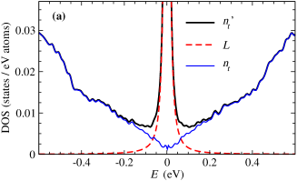
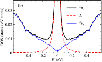
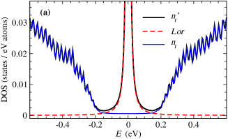
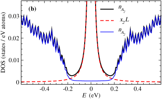
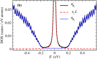
As explained in the paper, with TB1 model and a - bipartite lattice, vacancies in the sublattice involve midgap states, at energy , that are located on sublattice. Because of the convolution with the Lorentzian (12), the calculated total DOS and average local DOS , A1, B1, A2, B2 can be written as
| (14) |
and
| (15) |
where () is proportional of the concentration of vacant atoms, () is the calculated DOS due to midgap states, and () is the DOS (LDOS) without the midgap states. () is computed by recursion method from equation (11) with meV, and () is computed from () by equation (14) (equation (15)). The total DOSs , shown in the main paper figures 2(1.a) and 2(1.b) (see also figures S3(a.1) and S3(b.1)), correspond respectively to total DOSs shown figures S3(a.1) and S3(b.1). Showing instead of allows to discuss more explicitly the DOS around and to show the presence of quasi-gap. This quasi-gap is hidden by the midgap state Lorentzian in DOS . Figures S4 and S5 show several examples of the three terms of equations (14)-(15). With A2 vacant atoms (figure S3(a.2) and figure S4), the midgap states ( term in equations (14-15)) are located on B2 sublattice. With B2 vacant atoms (figure S3(b.2) and figure S5), the midgap states are located both on A2 sublattice and B1 sublattice.
3. Eigenstates of a square bipartite lattice with vacancies in a sublattice
In this section, we consider a simple square lattice containing two atoms in a unit cell: atom A in position and atom B in position . Only orbitals are taken into account and the Hamiltonian includes only nearest-neighbor hopping between orbitals:
| (16) |
where and create and annihilate respectively an electron on the orbital located at , is the sum on index and with , and is the hopping matrix element between two orbitals located at and . Each atom A is coupled with only B atoms and reciprocally. This lattice is thus a bipartite lattice with two equivalent sub-parts and corresponding respectively to atoms A and atoms B.
We consider vacancies (missing atoms) distributed randomly in the A sublattice. As explained in previous section (section 2), we calculated DOS, , (total), A, B (figure S6(a)) and the DOS , , (figure S6(b)). The Lorentzian of the midgap states at is clearly seen on total DOS, , and average local DOS, , on the B sublattice. As expected from the bipartite analysis explained in the paper, vacancies in a sublattice result in a gap between and . The energy gap increases as the concentration of vacancies increases (figures S6(c,d)).
These calculations are performed by recursion in a supercell (section 2) containing atoms. Figures S6(a,b,c) presents DOS calculated with meV. In this case, the convolution with the Lorentzian of width hides the gap when the concentration of vacancies is small. To check the presence of real gap, we show DOS calculated with meV in figure S6(d). In this case, gap in clearly seen at all calculated vacancy concentrations, but unphysical oscillations appeared in DOSs. Those oscillations are due to numerical artifact related to the termination of the continuous fraction expansion of the Green function (equation (11)) in presence of a gap [47].
4. Numerical method for conductivity
4.1. Kubo-Greenwood scheme
In Kubo-Greenwood formula for transport properties, the quantum diffusion , is computed by using the polynomial expansion of the average square spreading, , for charge carriers. This method, developped by Mayou, Khanna, Roche and Triozon [48, 49, 50, 51, 52], allows very efficient numerical calculations by recursion in real-space that taken into account all quantum effects. It has been used to studies quantum transport in disordered graphene [28, 34, 33, 59, 60, 57, 37] and chemically doped graphene [61, 30]. Static defects are included directly in the structural modelisation of the system and they are randomly distributed on a supercell containing up to Carbon atoms. This corresponds to typical sizes of about one micrometer square which allows to study systems with inelastic mean-free length of the order of few hundreds nanometers. Inelastic scattering is computed [37] within the Relaxation Time Approximation. An inelastic scattering time beyond which the propagation becomes diffusive due to the destruction of coherence by inelastic process. One finally get the Einstein conductivity formula (at K), [37]
| (17) |
where is the Fermi level, is the diffusivity (diffusion coefficient at energy and inelastic scattering time ),
| (18) |
is the density of states (DOS) and is the inelastic mean-free path. is the typical distance of propagation during the time interval for electrons at energy ,
| (19) |
Without static defects (static disorder) the and goes to infinity when diverges. With statics defects, at every energy , reaches a maximum value,
| (20) |
called microscopic conductivity. corresponds to the usual semi-classical approximation (semi-classical conductivity). This conductivity is typically the conductivity at room temperature, when inelastic scattering (inelastic mean free path ) is closed to elastic scattering (elastic mean free path ), and , where is the maximum value of at energy and the velocity at very small times (slope of ).
For larger and , and , quantum interferences may result in a diffusive state, , or a sub-diffusive state where decreases when and increase. For very large , closed to localization length , the conductivity goes to zero. These two last regimes (, and ), which correspond to the low temperature regime, are not discussed in the main paper.
4.2. Midgap states in case of first neighbor hopping model (TB1) with vacancies on a sublattice only
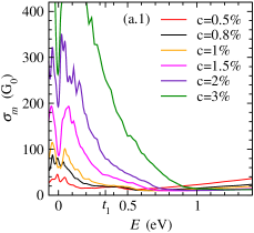
As discussed section 2, with first neighbor hopping model (TB1) and vacancies in only one sublattice, midgap states are found at the energy . These states are not coupled to each other by ; thus they do not contributed to the DOS and the conduction properties at . For this reason, the conductivity presented in the main paper is computed numerically by equation (20) using the total DOS that does not included the Lorentzian due to midgap states at (section 2 of this Supplementary Material). Microscopic conductivity computed with and without this Lorentzian contribution to the DOS is shown figure S7.
Therefore our study does not deal with conduction by midgap states at in the case of first neighbor hopping model (TB1). Nevertheless the results with the more realistic Hamiltonian TB2, that includes hopping beyond first neighbor, show that midgap states in TB1 model are very specific to TB1 model and are not realistic in real bilayer graphene, as it has been found for the monolayer graphene [38].
References
References
- [1] K. S. Novoselov, A. K. Geim, S. V. Morozov, D. Jiang, Y. Zhang, S. V. Dubonos, I. V. Grigorieva, and A. A. Firsov. Electric field effect in atomically thin carbon films. Science, 306(5696):666–669, 2004.
- [2] Claire Berger, Zhimin Song, Tianbo Li, Xuebin Li, Asmerom Y. Ogbazghi, Rui Feng, Zhenting Dai, Alexei N. Marchenkov, Edward H. Conrad, Phillip N. First, and Walt A. de Heer. Ultrathin epitaxial graphite: 2d electron gas properties and a route toward graphene-based nanoelectronics. The Journal of Physical Chemistry B, 108(52):19912–19916, 2004.
- [3] Ayako Hashimoto, Kazu Suenaga, Alexandre Gloter, Koki Urita, and Sumio Iijima. Direct evidence for atomic defects in graphene layers. Nature, 430(4):870, 2004.
- [4] Yuanbo Zhang, Yan-Wen Tan, Horst L. Stormer, and Philip Kim. Experimental observation of the quantum hall effect and berry's phase in graphene. Nature, 438(4):201, 2005.
- [5] Xiaosong Wu, Xuebin Li, Zhimin Song, Claire Berger, and Walt A. de Heer. Weak antilocalization in epitaxial graphene: Evidence for chiral electrons. Phys. Rev. Lett., 98(4):136801, 2007.
- [6] S. Y. Zhou, D. A. Siegel, A. V. Fedorov, and A. Lanzara. Metal to insulator transition in epitaxial graphene induced by molecular doping. Phys. Rev. Lett., 101(4):086402, 2008.
- [7] John P. Robinson, Henning Schomerus, László Oroszlány, and Vladimir I. Fal’ko. Adsorbate-limited conductivity of graphene. Phys. Rev. Lett., 101(4):196803, 2008.
- [8] A. H. Castro Neto, F. Guinea, N. M. R. Peres, K. S. Novoselov, and A. K. Geim. The electronic properties of graphene. Rev. Mod. Phys., 81(0):109–162, 2009.
- [9] Jian-Hao Chen, W. G. Cullen, C. Jang, M. S. Fuhrer, and E. D. Williams. Defect scattering in graphene. Phys. Rev. Lett., 102(4):236805, 2009.
- [10] Aaron Bostwick, Jessica L. McChesney, Konstantin V. Emtsev, Thomas Seyller, Karsten Horn, Stephen D. Kevan, and Eli Rotenberg. Quasiparticle transformation during a metal-insulator transition in graphene. Phys. Rev. Lett., 103(4):056404, 2009.
- [11] Z. H. Ni, L. A. Ponomarenko, R. R. Nair, R. Yang, S. Anissimova, I. V. Grigorieva, F. Schedin, P. Blake, Z. X. Shen, E. H. Hill, K. S. Novoselov, and A. K. Geim. On resonant scatterers as a factor limiting carrier mobility in graphene. Nano Lett., 10(10):3868–3872, 2010.
- [12] Shu Nakaharai, Tomohiko Iijima, Shinichi Ogawa, Shingo Suzuki, Song-Lin Li, Kazuhito Tsukagoshi, Shintaro Sato, and Naoki Yokoyama. Conduction tuning of graphene based on defect-induced localization. ACS Nano, 7(7):5694–5700, 2013.
- [13] Pei-Liang Zhao, Shengjun Yuan, Mikhail I. Katsnelson, and Hans De Raedt. Fingerprints of disorder source in graphene. Phys. Rev. B, 92(8):045437, 2015.
- [14] M. Barrejon, A. Primo, M. J. Gomez-Escalonilla, Jose Luis G. Fierro, H. Garcia, and F. Langa. Covalent functionalization of n-doped graphene by n-alkylation. Chem. Commun., 51(4):16916–16919, 2015.
- [15] Aires Ferreira, J. Viana-Gomes, Johan Nilsson, E. R. Mucciolo, N. M. R. Peres, and A. H. Castro Neto. Unified description of the dc conductivity of monolayer and bilayer graphene at finite densities based on resonant scatterers. Phys. Rev. B, 83(22):165402, 2011.
- [16] Edward McCann and Mikito Koshino. The electronic properties of bilayer graphene. Reports on Progress in Physics, 76(5):056503, 2013.
- [17] Guy Trambly de Laissardière, Didier Mayou, and Laurence Magaud. Localization of dirac electrons in rotated graphene bilayers. Nano Letters, 10(3):804–808, 2010.
- [18] Guy Trambly de Laissardière, Didier Mayou, and Laurence Magaud. Numerical studies of confined states in rotated bilayers of graphene. Phys. Rev. B, 86(7):125413, 2012.
- [19] Guy Trambly de Laissardière, Omid Faizy Namarvar, Didier Mayou, and Laurence Magaud. Electronic properties of asymmetrically doped twisted graphene bilayers. Phys. Rev. B, 93(12):235135, 2016.
- [20] Dinh Van Tuan and Stephan Roche. Anomalous ballistic transport in disordered bilayer graphene: A dirac semimetal induced by dimer vacancies. Phys. Rev. B, 93(6):041403, 2016.
- [21] Ahmed Missaoui, Jouda Jemaa Khabthani, Nejm-Eddine Jaidane, Didier Mayou, and Guy Trambly de Laissardière. Numerical analysis of electronic conductivity in graphene with resonant adsorbates: comparison of monolayer and bernal bilayer. The European Physical Journal B, 90(4):75, Apr 2017.
- [22] Taisuke Ohta, Aaron Bostwick, Thomas Seyller, Karsten Horn, and Eli Rotenberg. Controlling the electronic structure of bilayer graphene. Science, 313(5789):951–954, 2006.
- [23] Yuanbo Zhang, Tsung-Ta Tang, Caglar Girit, Zhao Hao, Michael C. Martin, Alex Zettl, Michael F. Crommie, Y. Ron Shen, and Feng Wang. Direct observation of a widely tunable bandgap in bilayer graphene. Nature, 459(4):820, 2009.
- [24] Adam A. Stabile, Aires Ferreira, Jing Li, N. M. R. Peres, and J. Zhu. Electrically tunable resonant scattering in fluorinated bilayer graphene. Phys. Rev. B, 92(5):121411, 2015.
- [25] Søren Ulstrup, Jens Christian Johannsen, Federico Cilento, Jill A. Miwa, Alberto Crepaldi, Michele Zacchigna, Cephise Cacho, Richard Chapman, Emma Springate, Samir Mammadov, Felix Fromm, Christian Raidel, Thomas Seyller, Fulvio Parmigiani, Marco Grioni, Phil D. C. King, and Philip Hofmann. Ultrafast dynamics of massive dirac fermions in bilayer graphene. Phys. Rev. Lett., 112(5):257401, 2014.
- [26] Long Ju, Zhiwen Shi, Nityan Nair, Yinchuan Lv, Chenhao Jin, Jairo Velasco Jr, Claudia Ojeda-Aristizabal, Hans A. Bechtel, Michael C. Martin, Alex Zettl, James Analytis, and Feng Wang. Topological valley transport at bilayer graphene domain walls. Nature, 520(6):650, 2015.
- [27] A. V. Rozhkov, A. O. Sboychakov, A.L. Rakhmanov, and Franco Nori. Electronic properties of graphene-based bilayer systems. Physics Reports, 648(132):1–104, 2016.
- [28] Aurélien Lherbier, Blanca Biel, Yann-Michel Niquet, and Stephan Roche. Transport length scales in disordered graphene-based materials: Strong localization regimes and dimensionality effects. Phys. Rev. Lett., 100(4):036803, 2008.
- [29] Shengjun Yuan, Hans De Raedt, and Mikhail I. Katsnelson. Modeling electronic structure and transport properties of graphene with resonant scattering centers. Phys. Rev. B, 82(16):115448, 2010.
- [30] Nicolas Leconte, Joël Moser, Pablo Ordejón, Haihua Tao, Aurélien Lherbier, Adrian Bachtold, Francesc Alsina, Clivia M. Sotomayor Torres, Jean-Christophe Charlier, and Stephan Roche. Damaging graphene with ozone treatment: A chemically tunable metal−insulator transition. ACS Nano, 4(7):4033–4038, 2010.
- [31] Yuriy V. Skrypnyk and Vadim M. Loktev. Electrical conductivity in graphene with point defects. Phys. Rev. B, 82(9):085436, 2010.
- [32] Yuriy V. Skrypnyk and Vadim M. Loktev. Metal-insulator transition in hydrogenated graphene as manifestation of quasiparticle spectrum rearrangement of anomalous type. Phys. Rev. B, 83(7):085421, 2011.
- [33] N. Leconte, A. Lherbier, F. Varchon, P. Ordejon, S. Roche, and J.-C. Charlier. Quantum transport in chemically modified two-dimensional graphene: From minimal conductivity to anderson localization. Phys. Rev. B, 84(12):235420, 2011.
- [34] Aurélien Lherbier, Simon M.-M. Dubois, Xavier Declerck, Stephan Roche, Yann-Michel Niquet, and Jean Christophe Charlier. Two-dimensional graphene with structural defects: Elastic mean free path, minimum conductivity, and anderson transition. Phys. Rev. Lett., 106(4):046803, 2011.
- [35] Guy Trambly de Laissardière and Didier Mayou. Electronic transport in graphene: Quantum effects and role of loacl defects. Modern Physics Letters B, 25(10):1019–1028, 2011.
- [36] Aurélien Lherbier, Simon M.-M. Dubois, Xavier Declerck, Yann-Michel Niquet, Stephan Roche, and Jean-Christophe Charlier. Transport properties of graphene containing structural defects. Phys. Rev. B, 86(18):075402, 2012.
- [37] Guy Trambly de Laissardière and Didier Mayou. Conductivity of graphene with resonant and nonresonant adsorbates. Phys. Rev. Lett., 111(5):146601, 2013.
- [38] Guy Trambly de Laissardière and Didier Mayou. Conductivity of graphene with resonant adsorbates: beyond the nearest neighbor hopping model. Advances in Natural Sciences: Nanoscience and Nanotechnology, 5(1):015007, 2014.
- [39] Fernando Gargiulo, Gabriel Autès, Naunidh Virk, Stefan Barthel, Malte Rösner, Lisa R. M. Toller, Tim O. Wehling, and Oleg V. Yazyev. Electronic transport in graphene with aggregated hydrogen adatoms. Phys. Rev. Lett., 113(6):246601, 2014.
- [40] Shengjun Yuan, T. O. Wehling, A. I. Lichtenstein, and M. I. Katsnelson. Enhanced screening in chemically functionalized graphene. Phys. Rev. Lett., 109(5):156601, 2012.
- [41] Wei Yan, Si-Yu Li, Long-Jing Yin, Jia-Bin Qiao, Jia-Cai Nie, and Lin He. Spatially resolving unconventional interface landau quantization in a graphene monolayer-bilayer planar junction. Phys. Rev. B, 93(6):195408, 2016.
- [42] Zhemi Xu, Zhimin Ao, Dewei Chu, and Sean Li. Uv irradiation induced reversible graphene band gap behaviors. J. Mater. Chem. C, 4(7):8459–8465, 2016.
- [43] Vitor M. Pereira, F. Guinea, J. M. B. Lopes dos Santos, N. M. R. Peres, and A. H. Castro Neto. Disorder induced localized states in graphene. Phys. Rev. Lett., 96(4):036801, 2006.
- [44] Vitor M. Pereira, J. M. B. Lopes dos Santos, and A. H. Castro Neto. Modeling disorder in graphene. Phys. Rev. B, 77(17):115109, 2008.
- [45] T. O. Wehling, S. Yuan, A. I. Lichtenstein, A. K. Geim, and M. I. Katsnelson. Resonant scattering by realistic impurities in graphene. Phys. Rev. Lett., 105(4):056802, 2010.
- [46] F. Ducastelle. Electronic structure of vacancy resonant states in graphene: A critical review of the single-vacancy case. Phys. Rev. B, 88(10):075413, 2013.
- [47] In D. G. Pettifor and D. L. Weaire, editors, The Recursion Method and Its Applications, Berlin, Heidelberg, 1987. Springer Berlin Heidelberg.
- [48] D. Mayou. Calculation of the conductivity in the short-mean-free-path regime. EPL (Europhysics Letters), 6(6):549, 1988.
- [49] D. Mayou and S. N. Khanna. A real-space approach to electronic transport. J. Phys. I Paris, 5(9):1199–1211, 1995.
- [50] S. Roche and D. Mayou. Conductivity of quasiperiodic systems: A numerical study. Phys. Rev. Lett., 79(4):2518–2521, 1997.
- [51] Stephan Roche and Didier Mayou. Formalism for the computation of the rkky interaction in aperiodic systems. Phys. Rev. B, 60(7):322–328, 1999.
- [52] François Triozon, Julien Vidal, Rémy Mosseri, and Didier Mayou. Quantum dynamics in two- and three-dimensional quasiperiodic tilings. Phys. Rev. B, 65(4):220202, 2002.
- [53] Supplementary material.
- [54] I. Brihuega, P. Mallet, H. González-Herrero, G. Trambly de Laissardière, M. M. Ugeda, L. Magaud, J. M. Gómez-Rodríguez, F. Ynduráin, and J.-Y. Veuillen. Unraveling the intrinsic and robust nature of van hove singularities in twisted bilayer graphene by scanning tunneling microscopy and theoretical analysis. Phys. Rev. Lett., 109(5):196802, 2012.
- [55] V. Cherkez, G. Trambly de Laissardière, P. Mallet, and J.-Y. Veuillen. Van hove singularities in doped twisted graphene bilayers studied by scanning tunneling spectroscopy. Phys. Rev. B, 91(7):155428, 2015.
- [56] N. M. R. Peres, F. Guinea, and A. H. Castro Neto. Electronic properties of disordered two-dimensional carbon. Phys. Rev. B, 73(23):125411, 2006.
- [57] Alessandro Cresti, Frank Ortmann, Thibaud Louvet, Dinh Van Tuan, and Stephan Roche. Broken symmetries, zero-energy modes, and quantum transport in disordered graphene: From supermetallic to insulating regimes. Phys. Rev. Lett., 110(5):196601, 2013.
- [58] Ahmed Missaoui. Study of quantum transport properties in two-dimensional systems Carbon-based: Graphene, organic semiconductors. PhD thesis, Faculté des Sciences Mathématiques, Physiques et Naturelles de Tunis, Sep 2017.
- [59] Nicolas Leconte, David Soriano, Stephan Roche, Pablo Ordejon, Jean-Christophe Charlier, and J. J. Palacios. Magnetism-dependent transport phenomena in hydrogenated graphene: From spin-splitting to localization effects. ACS Nano, 5(5):3987–3992, 2011. PMID: 21469688.
- [60] Stephan Roche, Nicolas Leconte, Frank Ortmann, Aurélien Lherbier, David Soriano, and Jean-Christophe Charlier. Quantum transport in disordered graphene: A theoretical perspective. Solid State Communications, 152(15):1404 – 1410, 2012. Exploring Graphene, Recent Research Advances.
- [61] Aurélien Lherbier, X. Blase, Yann-Michel Niquet, Fran çois Triozon, and Stephan Roche. Charge transport in chemically doped 2d graphene. Phys. Rev. Lett., 101:036808, Jul 2008.