Stable Ultra-thin CdTe Crystal: A Robust Direct Gap Semiconductor
Abstract
Employing density functional theory based calculations, we investigate structural, vibrational and strain-dependent electronic properties of an ultra-thin CdTe crystal structure that can be derived from its bulk counterpart. It is found that this ultra-thin crystal has an 8-atom primitive unit cell with considerable surface reconstructions. Dynamic stability of the structure is predicted based on its calculated vibrational spectrum. Electronic band structure calculations reveal that both electrons and holes in single layer CdTe possess anisotropic in-plane masses and mobilities. Moreover, we show that the ultra-thin CdTe has some interesting electromechanical features, such as strain-dependent anisotropic variation of the band gap value, and its rapid increase under perpendicular compression. The direct band gap semiconducting nature of the ultra-thin CdTe crystal remains unchanged under all types of applied strain. With a robust and moderate direct band gap, single-layer CdTe is a promising material for nanoscale strain dependent device applications.
pacs:
77.65.-j, 73.61.Ga, 73.22.-f, 71.15.MbI Introduction
Discovery of grapheneNovoselov has attracted great interest towards the family of two-dimensional (2D) crystal structures. In addition to graphene, other 2D crystals such as germanene,Cahangirov ; Bianco silicene,Vogt ; Sahin stanene,Zhu ; Rachel transition-metal dichalcogenides (TMDs),Wang ; Esfahani ; Island ; Chuang ; Kang and post-transition-metal chalcogenides (TMCs)Late ; Cai ; Yagmurcukardes have been predicted and successfully synthesized. One of the most prominent members of 2D crystals is MoS2. MoS2 exhibits a transition from an indirect band gap of 1.29 eV to a direct band gap of 1.90 eV when its layer thickness is reduced from bulk to a single-layer.Mak ; Splendiani Single-layer MoS2 based field-effect transistors (FETs) can have room-temperature on/off ratios of the order of 108 and these fabricated transistors can exhibit a carrier mobility larger than 200 cm2(V s).Radisavljevic ; Radisavljevic1 Moreover, MoS2 has excellent mechanical properties like high flexibilityPu ; Lee and high strength.Bertolazzi Due to these outstanding properties, 2D materials will play an important role in the applications of future optoelectronics and flexible electronics.
Recent studies have shown that not only layered materials but also ultra-thin forms of non-layered materials that consist of a few atomic layer thickness can form 2D crystals.Tan ; Vogt ; Bacaksiz For instance, CdSe, CdS and CdTe nanoplatelets with thicknesses ranging from 4 to 11 monolayers were synthesized.Ithurria The thickness dependence of the absorption and emission spectra of these nanoplatelets were demonstrated. Park et al. achieved successful synthesis of 1.4-nm-thick ZnSe nanosheets with wurtzite structure.Park Using a colloidal template method large-scale fabrication of free-standing ultra-thin and lamellar-structured CdSe with wurtzite crystal structure was achieved.Son Furthermore, using a lamellar hybrid intermediate, large-area, free-standing, single-layers of ZnSe were fabricated.Sun Single-layers of ZnSe-pa (pa stands for n-propylamine) were exfoliated from a lamellar hybrid (Zn2Se2)(pa) intermediate. Then, by heat treatment pa-molecules were cleared off and the colloidal suspension of clean ZnSe single-layers was obtained. Fabricated single-layer ZnSe has four-atomic-layer thickness. They showed that, produced single-layer ZnSe was highly stable over several days. The photocurrent densities of these monolayers are much higher than that of their bulk counterparts.
Cadmium telluride (CdTe) is one of the most popular II-VI semiconductors because of its potential applications in optoelectronic devices such as photodetectors, solar cells and room temperature X- and gamma-ray detectors.Rogalski ; Gupta ; Tu ; Szeles CdTe has a direct optical band gap of 1.5 eV with a high absorption coefficient.Ferekides ; Mahabaduge Solar cell efficiency of CdTe-based thin-films has recently reached 22.1%.Green CdTe crystallizes in the zinc-blende structure at room temperature. The CdTe thin films can be grown by various deposition techniques such as chemical vapor deposition,Kim pulsed laser deposition,Diamant electrochemical depositionBonilla and spray pyrolysis.Ison Generally, the intrinsic properties of ultra-thin materials exhibit drastic changes compared to their bulk counterparts. Thus, when a material is thinned from bulk to ultra-thin form, it can exhibit enhanced properties and new functionalities.
In this study, motivated by the recent synthesis of ultra-thin II-VI binary compounds, we investigate structural, electronic and vibrational properties of single-layer CdTe using first principle calculations based on density functional theory (DFT). Although there are a few prior computational studies on single-layer CdTe,Wang1 ; Zheng free-standing monolayer CdTe has not been predicted yet. We found that single-layer CdTe containing eight atoms in the primitive unit cell is structurally stable with anisotropic electronic properties. It has a direct band-gap at the point and direct gap transition at the point is not affected by strain along any direction. The strain-dependent anisotropic variation of the band gap value and its rapid increase under out-of-plane compression pressure are found. The paper is organized as follows: details of the computational methodology are given in Sec. II. Structural and electronic properties of single-layer CdTe are presented in Sec. III. In Sec. IV, the dynamical stability of single-layer CdTe is studied. Effect of strain on electronic properties is discussed in Sec. V. Finally, we outline our results in Sec. VI.
II Computational Methodology
All calculations were performed within the density functional theory (DFT) using projector-augmented-wave potentials (PAW) and a plane-wave basis set as implemented in the Vienna ab initio simulation package (VASP).Kresse ; Kresse1 Perdew-Burke-Ernzerhof (PBE) version of generalized gradient approximation (GGA)Perdew was used for the description of the exchange-correlation functional. Analysis of the charge transfers in the structures was made by the Bader technique.Henkelman The ionization energy is determined as the energy difference between the valance band maximum energy and the vacuum level at the (110) side of the bulk and single-layer CdTe.
The conjugate gradient algorithm was used to optimize the structure. The cutoff energy for the plane-waves was chosen to be 500 eV. The convergence criterion for energy was taken to be 10-5 eV between two consecutive steps. The convergence for the Hellmann-Feynman force in each unit cell was taken to be 10-4 eVÅ. The pressure in the unit cell was kept below 1 kBar. In order to eliminate interlayer interaction within the periodic images, a vacuum spacing of approximately 12 Å between adjacent layers was chosen. For the structural optimization, a 9121 -centered k-point mesh was used. The cohesive energy per atom was calculated using the formula
| (1) |
where ECd and ETe are isolated single atom energies for Cd and Te, respectively. While stands for the number of all atoms, and show the numbers of Cd and Te atoms in the unit cell, respectively. ESL denotes the total energy of the single-layer CdTe. Phonon dispersions and eigenvectors are calculated by making use of the small displacement methodology implemented in the PHON code.Alfe
| dCd-Te | Ec | Egap | I. E. | ||||
|---|---|---|---|---|---|---|---|
| (Å) | (Å) | (Å) | (e) | (eV) | (eV) | (eV) | |
| Bulk CdTe | 6.52 | - | 2.82 | 0.5 | 2.20 | 0.72 | 5.22 |
| SL CdTe | 6.18 | 4.53 | 2.77-2.90 | 0.5 | 1.79 | 1.42 | 5.15 |
III Structural and Electronic Properties of Single-Layer CdTe
It is well-known that the bonding character of zinc-blende CdTe is partly covalent and partly ionic.Groiss ; Guo Except for the (110) facets, zinc-blende structure of CdTe has polar surfaces, which are chemically highly active. Even if single-layer structures having these polar surfaces could be obtained, their chemical activity would hinder their stability. However, since the (110) surfaces are non-polar, cleavage along these planes could be more feasible.
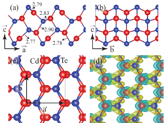
The proposed structure of CdTe single-layers in our study have the same crystal structure as the fabricated highly stable single-layer of zinc-blende ZnSe (zb-ZnSe).Sun Side views along and directions and top view of single-layer CdTe are shown in Figs. 1 (a)-(c), respectively. Lattice parameters of single-layer CdTe are found to be a 6.18 and b 4.53 Å. Calculated lattice parameters are smaller than those for bulk CdTe which is 6.52 Å. Fig. 1 (a) shows that the Cd-Te bond lengths vary from 2.77 to 2.90 Å, bond lengths between surface atoms being smaller than those of the inner atoms in the layer. As seen in Fig. 1 (b), Te atoms are at the surfaces of the layer, and each surface Te atom binds to three Cd atoms. The inner Te atoms are surrounded by 4 Cd atoms with tetrahedral type bonds. During the atomic relaxation of the truncated layer, Cd atoms that are at the surface recede toward the inner Te atoms; remaining Te atoms move outward. Such reconstructions stabilize the layer surfaces.
Bader charge analysis reveals that each Cd atom donates 0.5e to each Te atom. To illustrate the charge transfer mechanism three dimensional charge density differences are shown in Fig. 1 (d). The charge density differences were calculated by subtracting charge of isolated Cd and Te atoms from charge of single-layer CdTe. The charge transfer between Cd and Te atoms resembles polar-covalent bonding. Due to a difference in the electronegativities of Cd and Te atoms (1.69 and 2.10 for Cd and Te atoms, respectively), the Cd-Te bonding has also some ionic character. Finally, the cohesive energy per atom of single-layer CdTe is 1.79 eV which is less than the bulk value of 2.20 eV per atom.
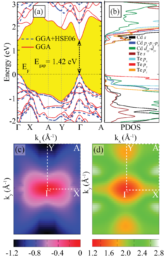
To investigate the full band dispersions and the characteristics of band edges in the Brillouin Zone (BZ), whole BZ energy-band structure is calculated and given in Fig. 2 (a). As shown in the figure, valence band maximum (VBM) and conduction band minimum (CBM) of CdTe reside at the same symmetry point of the . The calculated GGA electronic-band structure demonstrate that single-layer CdTe is a direct-gap semiconductor with a band gap of 1.42 eV. In order to give more accurate gap energy of the single-layer CdTe the calculated band structures within HSE06 correction are also shown Fig. 2 (a). A calculated HSE06 gap of single-layer CdTe is 2.13 eV. Since the trend and qualitative behavior of all the bands calculated using GGA and HSE06 are similar, only the GGA based results are given in the rest of the paper.
| me (L) | me (X) | me (Y) | me (A) | mh (L) | mh (X) | mh (Y) | mh (A) | |
|---|---|---|---|---|---|---|---|---|
| Bulk CdTe | 0.10 | 0.09 | - | - | 0.84 | 0.72 | - | - |
| SL CdTe | - | 0.39 | 0.17 | 0.21 | - | 0.74 | 0.14 | 0.20 |
In order to properly understand the electronic properties of CdTe, partial density of states (PDOS) is also plotted in Fig. 2 (b). The states in the vicinity of VBM are mostly composed of py orbitals of Te. These py orbitals of Te atoms are parallel to the b lattice vector of the unit cell. On the other hand, CBM is mostly made up of the s orbitals of Cd and the s and pz orbitals of Te. Note that, the pz orbital contribution of Te atom mainly comes from surface Te atoms. Two-dimensional contour plots of the valence band (VB) and the conduction band (CB) of the single-layer CdTe are shown in Figs. 2 (c) and (d). The directional anisotropy at the band edges is clearly seen in the surface plots. Ionization energy (I. E.) of single-layer and bulk CdTe surfaces are also calculated and are shown in Table 1.
Due to reduced crystal symmetry in a single layer form of a material, its electronic characteristics are quite different from their bulk forms. Moreover, in-plane anisotropy in the ultra-thin materials can lead to significant modifications in the electronic properties of the material. Therefore, the investigation of direction-dependent electronic properties of ultra-thin materials is of importance. The effective masses of electron (me) and hole (mh) of single-layer CdTe are calculated near the point. Our calculations show that the me and mh effective masses are highly anisotropic around the point. As given in Table 2 me values are 0.39, 0.17 and 0.21 for X, Y and A, respectively. mh values are 0.74, 0.14 and 0.20 for X, Y and A, respectively. As seen in Fig. 2 (b), the VBM is mainly composed of py electrons of Te atoms, thus this causes a high in-plane anisotropy in mh values. The anisotropy in the electron and hole masses are evident even from the crystal structure where x- and y-directions are highly anisotropic (see Fig. 1). For comparison, the calculated values of me and mh of bulk CdTe are also given in Table 2.
IV Dynamical Stability of Single-Layer CdTe
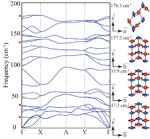
Dynamical stability of the single-layer CdTe is investigated by examining the phonon spectra of the crystal. The small displacement method as implemented in the PHON software package is used to calculate the phonon spectra.Alfe 441 supercell is used for the phonon-band structure calculations. In Fig. 3, we present the calculated phonon-band structure of single-layer CdTe obtained by the method described above. It is found that all the phonon modes have real eigenfrequencies, which indicate that CdTe single-layers are stable. The small imaginary frequencies (less than 1 cm-1) near the point are numerical artifacts caused by the inaccuracy of the FFT grid and they get cured as larger and larger supercells are considered.
The structural characteristics of bulk zb-CdTe were well studied in earlier Raman studies. The unit cell of bulk zb-CdTe consists of one Cd and one Te atoms, therefore the phonon dispersion of bulk CdTe yields three acoustic and three optical modes. Main Raman active phonon modes are transverse optical (TO) and longitudinal optical (LO) modes and they occur approximately at 141 and 168 cm-1.Amirtharaj In addition to these prominent modes, A1 and E symmetry modes were reported at 92, 103, 120 and 147 cm-1 which give information about the presence of Te on the surface of bulk CdTe.Amirtharaj ; Zitter
On the other hand, the unit cell of single-layer CdTe contains four Cd atoms and four Te atoms. Therefore, the phonon dispersion of single-layer CdTe possesses three acoustic and twenty-one optical modes as shown in Fig. 3. As pointed out in the previous section there is a relaxation of the top atomic layers in the single-layer CdTe and bond length of the surface atoms is shorter than bond length of the inner atoms. Distortions of surface atoms lead to several flat phonon bands in Fig. 3. These distortions lift the degeneracies at the point and lead to hybridization of the acoustic and optical phonon branches. Optical character and frequency of possible Raman active modes are shown in the right panel of Fig 3. The modes at 17.5, 35.9 and 137.2 cm-1 have in-plane character (Eg like) and the motion of the atoms are parallel to the . For the mode 137.2 cm-1, Cd and Te atoms move in opposite directions. However, atomic layers exhibit contour-phase motion for the modes 17.5 and 35.9 cm-1. The mode with the highest frequency of 178.3 cm-1 has mixed in-plane and out-of-plane character (Ag like) with Cd and Te atoms having counter-phase motion.
Due to the heavier atomic masses and more ionic electronic character, phonon modes of single-layer CdTe lie at much lower energies than phonon modes of other 2D materials such as graphene, hBN and TMDs. Moreover, it was reported that phonon modes of structurally similar material of single-layer ZnSe lie at more higher energies than that of single-layer CdTe.Bacaksiz Thus, it is clear that single-layer CdTe is a quite soft material.
V Strain Response of Single-Layer CdTe
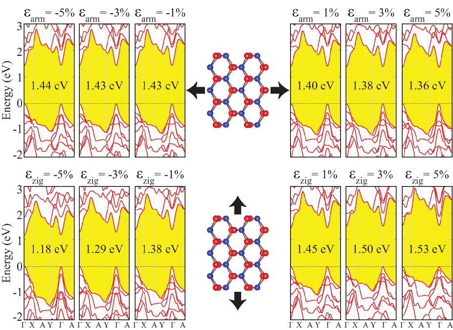
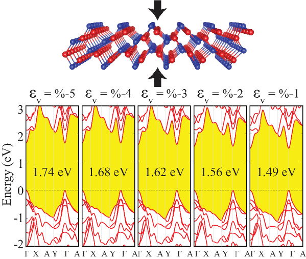
The built-in strain is inevitable as single-layer materials are usually grown on a substrate. It was shown that strain can significantly alter mechanical, electronic and magnetic properties of ultra-thin materials.Rodin ; Jiang ; Tao Thus, in this section the effects of out-of-plane compressive, in-plane compressive and tensile strains on the direct-gap semiconducting behavior of single-layer CdTe are examined. The lattice constants of the unit cell for in-plane compressive and tensile strains are changed up to 5% along zigzag (along ) and armchair (along ) directions. The thickness of the layer is compressed up to 5% for out-of-plane compressive strain calculations.
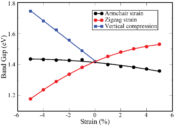
Fig. 4 illustrates the evolution of electronic band structures for strained CdTe single-layer. It is clearly seen that electronic characteristics of single-layer CdTe do not change significantly with applied in-plane strain. It exhibits robust direct-gap at the point under considered strain values. It is found that the band gap of single-layer CdTe is more sensitive to the in-plane strain applied along zigzag direction than armchair direction. With the increase of tensile strain along the armchair direction, the band gap of CdTe decreases, whereas the band gap increases when compressive strain along the armchair direction is increased. However, the increase of tensile strain along zigzag direction results in an increase in the band gap of CdTe, the increase of compressive strain leads to decrease in the band gap. Fig. 5 shows electronic band structures for single-layer of CdTe under compression along out-of-plane direction. It is found that CdTe does not show significant structural distortion under considered out-of-plane compression values. Direct gap character of CdTe at the point does not change, but the electronic band gap increases as applied compressive strain increases.
Variation of the band gap of single-layer CdTe crystal under out-of-plane and in-plane strains are shown in Fig. 6. It was already calculated that VBM of the CdTe is mainly composed of py orbitals of Te atoms. Since the Te-py orbitals are aligned in the zigzag direction, modification of band edges via applied strain occurs much faster than those in armchair direction. As shown in Fig. 6, while the band gap slowly decreases with increasing strain in armchair direction, it rapidly increases with increasing strain in zigzag direction.
Therefore, the variation of band gap of CdTe for applied tensile strain (in 5%) along armchair direction is fitted to an expression as
| (2) |
and are fitting parameters and their values are 0.008 and 0.001 eV. Compressive strain along the zigzag direction decreases the hybridization of py orbitals of Te atom and d orbitals of Cd atom at the VBM, whereas it increases the hybridization of Te and Cd orbitals at the CBM. Therefore, the VBM and CBM energies vary in opposite directions, thereby decreasing the band gap. The variation of band gap of single-layer CdTe for applied tensile strain along zigzag direction is fitted to an expression as
| (3) |
where and are fitting parameters and their values are 0.035 and 0.003 eV, respectively. As a result, strain-dependence of the band gap of single-layer CdTe exhibits nonlinear variations behavior when an in-plane strain is applied.
The out-of-plane strain application can easily alter the interlayer spacing of layered materials and therefore it provides an efficient way of tuning the electronic properties. In the Sec. III we found that the CBM of CdTe is dominated by pz orbitals of Te atom. Therefore, application of compressive out-of-plane strain significantly affects the hybridization between orbitals of Cd and Te. Consequently, the band gap of CdTe increases monotonically with increasing compressive strain along out-of-plane direction and the rate of change for band gaps is faster for the out-of-plane strain than that of in-plane strains. Increasing behavior of band gap of CdTe for applied compressive strain along out-of-plane direction is fitted to an expression as
| (4) |
is a fitting parameter and it has a value of 0.065 eV.
It appears that while the direct band gap feature is maintained, controllable modification of the band gap values of monolayer CdTe is feasible by the application of uniaxial strain along different crystallographic orientations. Mostly, electronic properties of ultra-thin materials are highly sensitive to the applied strain. It was shown that strain changes the energy dispersion, band gap, and the band edges of graphene.Wong In another study, the optical band gap of MoS2 experiences a direct-to-indirect transition with applied strain, which decreases the measured photoluminescence intensity.Conley Previously we showed that electronic band structure of single-layer MoSe2 undergoes a direct to indirect band gap crossover under tensile strain.Horzum Moreover, strain induced phase transition (from semiconducting 2H phase to metallic 1T’ phase) is observed in MoTe2.Song Therefore, in contrast to typical ultra-thin materials, monolayer CdTe exhibits robust and moderate band gap that covers the broad range of the solar spectrum, which are essential for its utilization in future electronics.
VI Conclusions
In this study, we investigated structural, phonon and electronic characteristics of single-layer CdTe by performing state-of-the-art first principle calculations. Structural analysis revealed that ultra-thin CdTe has a crystal structure made of reconstructed 8-atomic primitive unit cell. Electronic band dispersion calculations showed that single-layer CdTe has a direct band gap of 1.42 (GGA) eV at the point. Direction dependent energy band dispersions at the vicinity of VBM and CBM indicate that single-layer CdTe has anisotropic electronic and optical properties.
Moreover, it is seen that electronic characteristics of single-layer CdTe are more sensitive to in-plane strain applied along zigzag direction than armchair direction. Along the armchair direction, the higher the tensile strain, the smaller the bandgap. However, increasing the tensile strain along zigzag direction increases the band gap. In addition, when a compressive strain applied in out-of-plane direction, the rate of increase of the electronic bandgap is much faster. It is also found that the direct bandgap semiconducting behavior of the ultra-thin CdTe is not affected by compressive and tensile strain applied in in-plane or out-of-plane directions. Ultra-thin CdTe crystal with its strain-independent and robust direct bandgap is quite suitable material for nanoscale optoelectronic device applications.
References
- (1) K. S. Novoselov, A. K. Geim, S. V. Morosov, D. Jiang, M. I.Katsnelson, I. V. Grigorieva, S. V. Dubonos, and A. A. Firsov, Science 306, 666 (2004).
- (2) S. Cahangirov, M. Topsakal, E. Akturk, H. Sahin, S. Ciraci, Phys. Rev. Lett. 102, 236804 (2009).
- (3) E. Bianco, S. Butler, S. Jiang, O. D. Restrepo, W. Windl, and J. E. Goldberger, ACS Nano 7, 4414 (2013).
- (4) P. Vogt, P. D. Padova, C. Quaresima, J. Avila, E. Frantzeskakis, M. C. Asensio, A. Resta, B. Ealet, and G. L. Lay, Phys. Rev. Lett. 108, 155501 (2012).
- (5) H. Sahin, S. Cahangirov, M. Topsakal, E. Bekaroglu, E. Akturk, R. T. Senger, S. Ciraci, Phys. Rev. B 80, 155453 (2009).
- (6) F. -f. Zhu, W. -j. Chen, Y. Xu, C. -l. Gao, D. -d. Guan, C. -h. Liu, D. Qian, S. -C. Zhang, and J. -f. Jia, Nat. Mater. 14, 1020, (2015).
- (7) S. Rachel and M. Ezawa, Phys. Rev. B 89, 195303, (2014).
- (8) Q. H. Wang, K. K. -Zadeh, A. Kis, J. N. Coleman, and M. S. Strano, Nat. Nanotechnol. 7, 699, (2012).
- (9) D. N. Esfahani, O. Leenaerts, H. Sahin, B. Partoens, and F. M. Peeters, J. Phys. Chem. C 119, 10602, (2015).
- (10) J. O. Island, A. Kuc, E. H. Diependaal, R. Bratschitsch, H. S. J. van der Zant, T. Heine, and A. C. -Gomez, Nanoscale, 8, 2589 (2016).
- (11) H. -J. Chuang, B. Chamlagain, M. Koehler, M. M. Perera, J. Yan, D. Mandrus, D. Tomanek, and Z. Zhou, Nano Lett. 16, 1896 (2016).
- (12) J. Kang, H. Sahin, and F. M. Peeters, Phys. Chem. Chem. Phys. 17, 27742 (2015).
- (13) D. J. Late, B. Liu, J. Luo, A. Yan, H. S. S. R. Matte, M. Grayson, C. N. R. Rao, and V. P. Dravid, Adv. Mater. 24, 3549 (2012).
- (14) H. Cai, J. Kang, H. Sahin, B. Chen, A. Suslu, K. Wu, F. M. Peeters, X. Meng, and S. Tongay, Nanotech. 27, 065203 (2016).
- (15) M. Yagmurcukardes, R. T. Senger, F. M. Peeters, and H. Sahin, Phys. Rev. B 94, 245407 (2016).
- (16) K. F. Mak, C. Lee, J. Hone, J. Shan, T. F. Heinz, Phys. Rev. Lett. 105, 136805 (2010).
- (17) A. Splendiani, L. Sun, Y. Zhang, T. Li, J. Kim, C. -Y. Chim, G. Galli, and F. Wang, Nano Lett. 10, 1271 (2010).
- (18) B. Radisavljevic and A. Kis, Nat. Mater. 12, 815 (2013).
- (19) B. Radisavljevic, A. Radenovic, J. Brivio, V. Giacometti, and A. Kis, Nature Nanotech. 6, 147 (2011).
- (20) J. Pu, Y. Yomogida, K. -K. Liu, L. -J. Li, Y. Iwasa, and T. Takenobu, Nano Lett. 12, 4013 (2012).
- (21) G. -H. Lee, Y. -J. Yu, X. Cui, N. Petrone, C. -H. Lee, M. S. Choi, D. -Y. Lee, C. Lee, W. J. Yoo, K. Watanabe, T. Taniguchi, C. Nuckolls, P. Kim, and J. Hone, ACS Nano 7, 7931 (2013).
- (22) S. Bertolazzi, J. Brivio, and A. Kis, ACS Nano 5, 9703 (2011).
- (23) C. Tan and H. Zhang, Nat. Commun. 6, 7873 (2015).
- (24) C. Bacaksiz, R. T. Senger, and H. Sahin, Appl. Surf. Sci. 409, 426 (2017).
- (25) S. Ithurria, M. D. Tessier, B. Mahler, R. P. S. M. Lobo, B. Dubertret, and A. L. Efros, Nat. Mater. 10, 936 (2011).
- (26) H. Park, H. Chung, and W. Kim, Mater. Lett. 99, 172 (2013).
- (27) J. S. Son, X. -D. Wen, J. Joo, J. Chae, S. -i. Baek, K. Park, J. H. Kim, K. An, J. H. Yu, S. G. Kwon, S. -H. Choi, Z. Wang, Y. -W. Kim, Y. Kuk, R. Hoffmann, T. Hyeon, Angew. Chem. Int. Ed. 48, 6861 (2009).
- (28) Y. Sun, Z. Sun, S. Gao, H. Cheng, Q. Liu, J. Piao, T. Yao, C. Wu, S. Hu, S. Wei, and Y. Xie, Nat. Commun. 3, 1057 (2012).
- (29) A. Rogalski, Rep. Prog. Phys. 68, 2267 (2005).
- (30) A. Gupta, V. Parikh, and A. D. Compaan, Sol. En. Mat. and Sol. Cell 90, 2263 (2006).
- (31) C. -C. Tu and L. Y. Lin, App. Phys. Lett. 93, 163107 (2008).
- (32) C. Szeles, Phys. Status Solidi B 241, 783 (2004).
- (33) C. S. Ferekides, U. Balasubramanian, R. Mamazza, V. Viswanathan, H. Zhao, D. L. Morel, Sol. En. 77, 823 (2004).
- (34) H. P. Mahabaduge, W. L. Rance, J. M. Burst, M. O. Reese, D. M. Meysing, C. A. Wolden, J. Li, J. D. Beach, T. A. Gessert, W. K. Metzger, S. Garner, and T. M. Barnes, Appl. Phys. Lett. 106, 133501 (2015).
- (35) M. A. Green, K. Emery, Y. Hishikawa, W. Warta, and E. D. Dunlop, Prog. Photovolt. Res. Appl. 24, 905 (2016).
- (36) K. -C. Kim, H. J. Kim, S. -H. Suh, M. Carmody, S. Sivananthan, and J. -S. Kim, Journal of Elec. Materi. 39, 863 (2010).
- (37) R. Diamant, L. Ponce, M. Fernandez, and E. Jimenez, Appl. Phys. B 66, 639 (1998).
- (38) S. Bonilla and E. A. Dalchiele, Thin Solid Films 204, 397 (1991).
- (39) V. V. Ison, A. R. Rao, and V. Dutta, Solid State Sci. 11, 2003 (2009).
- (40) J. Wang, J. Meng, Q. Li, and J. Yang, Phys. Chem. Chem. Phys. 18, 17029 (2016).
- (41) H. Zheng, X. -B. Li, N. -K. Chen, S. -Y. Xie, W. Q. Tian, Y. Chen, H. Xia, S. B. Zhang, and H. -B. Sun, Phys. Rev. B 92, 115307 (2015).
- (42) G. Kresse and D. Joubert, Phys. Rev. B 59, 1758 (1999).
- (43) G. Kresse and J. Furthmuller, Phys. Rev. B 54, 11169 (1996).
- (44) J. P. Perdew, K. Burke, and M. Ernzerhof, Phys. Rev. Lett. 77, 3865 (1996).
- (45) G. Henkelman, A. Arnaldsson, and H. Jonsson, Comput. Mater. Sci. 36, 354 (2006).
- (46) D. Alfè, Comput. Phys. Commun. 180, 2622 (2009).
- (47) H. Groiss, G. Hesser, W. Heiss, F. Schäffler, R. Leitsmann, F. Bechstedt, K. Koike, and M. Yano, Phys. Rev. B 79, 235331 (2009).
- (48) L. Guo, S. Zhang, W. Feng, G. Hu, and W. Li, J. Alloys Compd. 579, 583 (2013).
- (49) A. Amirtharaj and F. H. Pollak, Appl. Phys. Lett. 45, 789 (1984).
- (50) R. N. Zitter, Surf. Sci. 28, 335 (1971).
- (51) A. S. Rodin, A. Carvalho, and A. H. C. Neto, Phys. Rev. Lett. 112, 176801 (2014).
- (52) J. -W. Jiang and H. S. Park, Nat. Comm. 5, 4727 (2014).
- (53) P. Tao, H. Guo, T. Yang, and Z. Zhang, J. Appl. Phys. 115, 054305 (2014).
- (54) J. -H. Wong, B. -R. Wu, and M. -F. Lin, J. Phys. Chem. C 116, 8271 (2012).
- (55) H. J. Conley, B. Wang, J. I. Ziegler, R. F. J. Haglund, S. T. Pantelides, K. I. Bolotin, Nano Lett. 13, 3626 (2013).
- (56) S. Horzum, H. Sahin, S. Cahangirov, P. Cudazzo, A. Rubio, T. Serin, and F. M. Peeters, Phys. Rev. B 87, 125415 (2013).
- (57) S. Song, D. H. Keum, S. Cho, D. Perello, Y. Kim, and Y. H. Lee, Nano Lett. 16, 188 (2016).