Room temperature magneto-optic effect in silicon light-emitting diodes
Abstract
In weakly spin-orbit coupled materials, the spin-selective nature of recombination can give rise to large magnetic-field effects, for example on the electro-luminescence of molecular semiconductors. While silicon has weak spin-orbit coupling, observing spin-dependent recombination through magneto-electroluminescence is challenging: silicon’s indirect band-gap causes an inefficient emission, and it is difficult to separate spin-dependent phenomena from classical magneto-resistance effects. Here we overcome these challenges and measure magneto-electroluminescence in silicon light-emitting diodes fabricated via gas immersion laser doping. These devices allow us to achieve efficient emission while retaining a well-defined geometry thus suppressing classical magnetoresistance effects to a few percent. We find that electroluminescence can be enhanced by up to 300% near room temperature in a seven Tesla magnetic field, showing that the control of the spin degree of freedom can have a strong impact on the efficiency of silicon LEDs.
Introduction
Spintronic effects in systems with weak spin-orbit coupling have attracted considerable attention due to their rich fundamental physics and potential for device applications 1; 2; 3; 4. A class of these effects can be measured optically 5; 6; 7, providing direct insight into phenomena such as spin-dependent recombination, where only the singlet state of an electron-hole pair can recombine radiatively back to the ground state. Since external magnetic fields can change the spin statistics and energy levels in the sample, magneto-electroluminescence (MEL) effects have been seen as the hallmark of spin-dependent recombination phenomena, and have given important insight into the role of spin in organic materials used for light-emitting diodes (LEDs) 8; 9; 10. These spintronic effects can then be harnesseed, to provide very senstive magnetic field sensors, sensible to external magentic fields of only a few mTesla comparable with the fluctuating hyperfine fields inside organic materials 11; 12; 13 or to engineer new light-emitting device architectures through reverse intersystem crossing 14.
Like molecular semiconductors, silicon has weak spin-orbit coupling, but emission is much less efficient due to silicon’s indirect band-gap, making analogous magneto-optic studies challenging, and requiring careful engineering to prepare efficient light-emitting diodes 15; 16; 17. In addition, observing spin-dependent magneto-electroluminescence in silicon requires that the magnetic field and device currents are parallel to effectively suppress classical magnetoresistance (MR) contributions which can enhance MR in silicon up to spectacular values even at room temperature 18; 19; 20; 21; 22.
Here we address both of these challenges by developing a new fabrication method for efficient silicon light-emitting diodes using an original doping technique, gas immersion laser doping (GILD), and investigate spin-dependent recombination in silicon LEDs (SiLEDs). The GILD process 23; 24; 25; 26 allows us to reach doping levels well beyond the solubility threshold which, as we describe below, gives rise to efficient emission, while retaining the well-defined planar geometry necessary to align electric and magnetic fields. Using our SiLEDs, we find that when classical MR effects are suppressed, electroluminescence can be substantially enhanced under a magnetic field near room temperature. We explain this phenomenon using a model of spin-dependent recombination 28; 29; 30 of electron-hole pairs and use our analysis to estimate the exchange energy of weakly bound excitons in silicon. Our experiments provide an optoelectronic approach to probe the spin statistics of carriers in silicon - a material which is an excellent candidate for scalable spin quantum computing 31; 32; 33. They also highlight the importance of controlling the spin degree of freedom for the efficiency of silicon light emitting devices.
Results
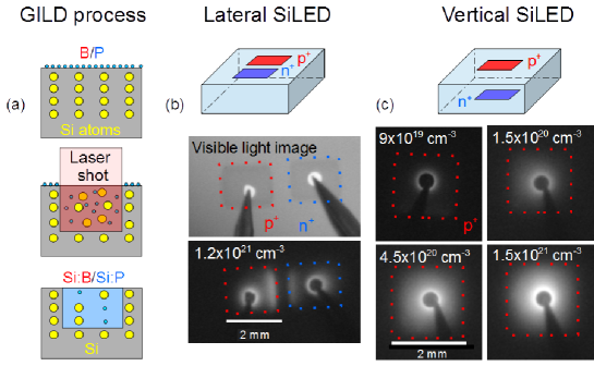
Description of the system: We start by describing the fabrication procedure of the GILD SiLEDs [Fig. 1-a] and the physical mechanism behind their enhanced efficiency, before discussing the MEL response of these devices. The Si light-emitting diodes were prepared by doping two spots with opposite polarities p+/n+ on a n-Si [100] substrate of resistivity and thickness using the GILD technique [Fig. 1-a]. A precursor gas for n+ (p+) doping is injected into an ultra-high vacuum chamber, where it saturates the chemisorbtion sites on the Si surface. The substrate is then melted by a pulsed excimer XeCl 308nm laser with a 25 ns pulse duration. The dopants diffuse into the liquid Si phase and are incorporated in the lattice as the liquid/solid interface moves back to the surface at the end of the irradiation 25. A Si:P/Si:B crystal is thus created by fast liquid phase epitaxy above the underlying Si substrate [Fig. 1-a]. The dose of active dopants is determined exclusively by the number of laser shots while the doping depth can be independently tuned by controlling the laser energy. Due to the short pulse duration and high recrystallization speed, high dopant concentrations beyond the solubility limit ( for Si:B) 27 can be reached without introducing defects. In our experiments, we varied the doping concentration in the range while keeping the doping depth constant at 80 nm (pulse energy ). Ti(15nm)/Al(200nm) electrodes were deposited on top of the doped spots after BHF deoxidation.
Device electroluminescence: We investigated EL from GILD SiLEDs in two different device geometries where the p+ and n+ spots were placed laterally, without overlap, on the same Si surface (Fig. 1-b) and in a vertical geometry where the n+/p+ were prepared on top of each other on opposite sides of the Si wafer (Fig. 1-c). The alignment between top and bottom spots in the vertical geometry was achieved by looking through the silicon wafer with an infrared camera which allowed to see the bottom GILD spots. This camera also allowed to record characterization images of EL devices. Images in the lateral geometry (Fig. 1-b) show that EL occurs mainly at the heavily doped GILD spots on both n+ and p+ sides whereas the undoped region in-between the two spots remains dark. This shows that EL is enhanced near the n+ and p+ interfaces as compared to bulk Si. This observation is supported by the strong improvement of the device brightness as the GILD doping concentration increases (see Fig. 1-c). The external quantum efficiency (EQE) for our brightest devices is around which is comparable with the highest reported values for devices without anti-reflection treatement 15.
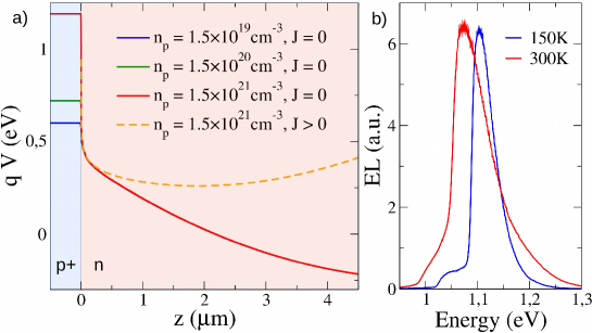
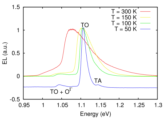
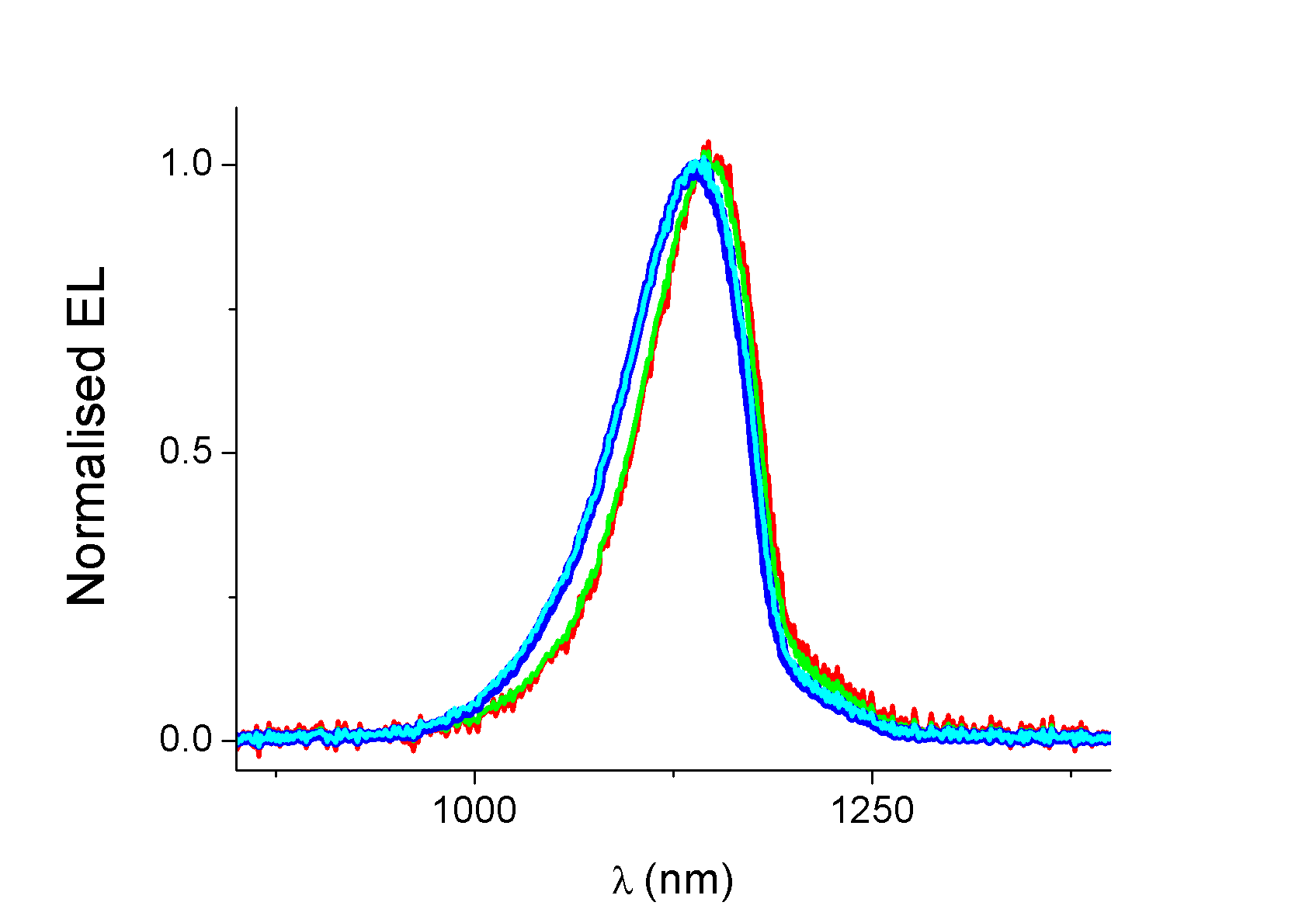
The physical origin of the EL enhancement can be understood from the electrostatic profile within the devices which we model using drift-diffusion simulations of the p+/n interface accounting for the Fermi-statistics in the highly doped regions 34. The simulated distributions of the electrostatic potential are shown on Fig. 2-a. In unbiased devices (see Supplementary Figure 1 for a more detailed discussion), the potential inside the region () is almost independent on the p+ doping concentration ; however a steep potential step forms at the p+/n interface, its height increasing with doping, creating a barrier that electrons have to overcome to leave the device. For parameters corresponding to the brightest devices the barrier is near an high and thermally activated transport is effectively prohibited. The p+ region thus plays the role of an electron blocking layer while the n+ region will similarly act as a hole blocking layer. Such layers are known to enhance the efficiency of organic LEDS 35; 36. When devices are biased the potential remains constant in the p+ region and near the p+/n interface as the applied potential will mainly drop across the intrinsic weakly doped regions which have much larger resistivity than the highly doped p+ region. A potential minimum therefore appears at sufficiently high forward bias near the p+/n and n/n+ interfaces. In these regions, located at a vertical distance of away from the interfaces, the internal electric field vanishes favoring radiative recombination since a built-in electric field would otherwise drive electron-hole pairs apart. Similarly the minority carriers (holes) predominantly recombine at the n+ interface as can be seen from the weaker EL observed from the n+ spot in lateral devices (see Fig. 1). Finally EL spectra in Fig. 2 (see also Supplementary Figure 2) are in very good agreement with previously reported lineshapes for bulk Si 37; 38; 39 in agreement with our model predicting emission in the weakly doped Silicon a micrometer away from the p+/n and n+/n interfaces.
SiLED Magneto-electroluminescence: Having described the structure of our devices and the physical mechanism behind their enhanced EL efficiency, we now use them to study the dependence of the EL on magnetic field in a vertical SiLED device (doping ); similar data was obtained on a device with doping. For this experiment devices where mounted inside an optical access magnet (Oxford instruments) and the EL was collected by a Ge photo-detector outside the cryostat. The SiLEDs were DC biased and the input of the Ge photo-detector was chopped at to enhance sensitivity.
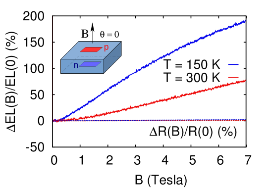
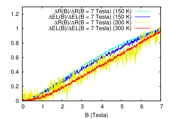
To study the role of spin in the MEL, we first applied a magnetic field perpendicular to the device surface, i.e. parallel to the internal electric field. We obtained a vanishing classical magetoresistance (MR), as shown in Fig. 3 where we observe only a weak residual MR in the 1% range both at and . The accuracy of this MR cancellation can seem surprising given the lack of electrical insulation around the spots. However, close to the onset voltage of the diode, the voltage drop mainly occurs accross the few micron wide depletion region between the p+ and n regions (the extent of the depletion region is shown on Fig. Supp. 1) and the current lines cannot bend significantly considering the large spot size 2mm 2mm. Fig. 3 also plots the MEL response, which shows a drastically different behaviour. Compared to the MR signal, the EL exhibits a two orders of magnitude stronger dependence on the magnetic field, with at room temperature and an even higher value at (for a 5 mA current). The striking difference in magnitude of the MEL signal over the MR suggests that the magnetic field is increasing radiative recombination. Since the EL quantum efficiency is low in silicon a strong change in EL has little effect on the total current, and hence the MR.
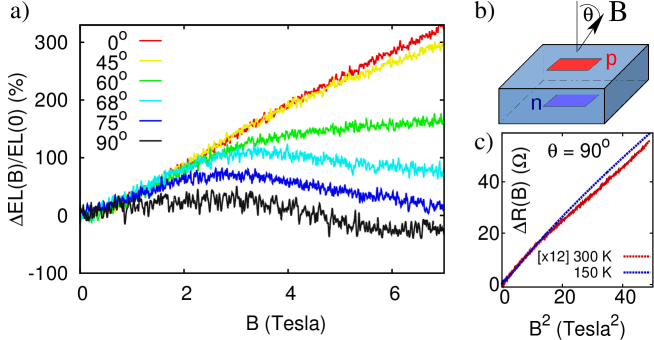
To further investigate the origin of the strong MEL effect in SiLEDs, we measured the MEL response as a function of the angle of the magnetic field relative to current lines Fig. 4. For moderate tilt angles below the MEL signal is nearly independent on the tilt. At larger tilt angles below , the MEL is unchanged at low-magnetic fields but decreases from the low tilt angle behaviour at high magnetic fields. We attribute this decrease to the magneto-diode effect 40; 41; 42: the in-plane component of the magnetic field bends electron and hole trajectories so that they cross a larger distance through the device and thus have a higher non radiative-recombination probability. A significant bending of current lines can occur in perpendicular electric and magnetic fields when the ratio between Hall and longitudinal mobility is large. This quantity is around at room temperature for and around at 150K (using the mobility values for a electron doped Si: at room temperature and at 150 K). The negative magneto-diode contribution to MEL is further enhanced in lateral devices with longer current paths through the sample (see Supplementary Figure 4), with a negative MEL amplitude comparable with the ratio .
The full MEL response is thus a superposition of a positive MEL component which depends only weakly on the -field direction, and a negative magneto-diode effect component which contributes more strongly at large tilt angles. A purely magnetodiode contribution would have the same dependence as the MR, which increases with the parallel magnetic field as , as expected from the Drude law (see Fig. 4), in contrast with the observed MEL signal which displays a linear dependence with except at the lowest fields. Since the angle and magnetic field dependence of the positive MEL effect are very different from the MR, we infer that the MEL is not determined by transport scattering times and may be related to spin-degrees of freedom.
Discussion
The MEL effect observed in SiLEDs when the current and magnetic field are parallel () can be explained as arising from the spin-dependent recombination of weakly bound electron-hole pairs within the devices, in analogy with the models developed by Kaplan et al. 28 and Merrifield 29. The ability of an electron-hole pair to recombine radiatively is determined by the overlap of the electron-hole pair wavefunction with the spin-zero singlet ground state - radiative recombination will only be efficient for electron-hole pairs in an singlet configuration, the recombination from an triplet electron-hole pair being much less efficient (Fig. 5-b). As the magnetic field is changed, the electron-hole eigenstates - which are in general not pure singlet or triplet spin states - are modified, altering their singlet overlap. As we explain below, this change in the electron-hole pair wavefunctions gives rise to a change in EL, and can explain the lineshapes observed experimentally. Importantly, this effect is independent of the direction of the magnetic field and can therefore describe the angular-dependent MEL observations (Fig. 4). We note that while spin-dependent free-carrier recombination has previously been studied through circularly polarised emission 49; 50; 51, here we invoke spin-dependent recombination of weakly bound exchange coupled electron-hole pairs to explain our MEL effects.
We start by considering the kinetic equation for the population of transient electron-hole pairs that are formed by brief collisions in the device recombination zone near room temperature. The population of transient pairs with spin-eigenstates is expected to follow the following rate equations:
| (1) |
Here is the electron-hole pair generation rate. The second term describes the probability of (spin-dependent) radiative recombination during collision events, with a rate . This term is proportional to the overlap of the electron-hole pair wavefunction with the spin-singlet state , where is the singlet state. The final (spin-independent) term reflects both the probability of escape from the shallow potential well where radiative recombination occurs in our devices and the rate of nonradiative relaxation. Solving this in steady-state for the total emission from the electon-hole pairs we find
| (2) |
where . This sum depends non-linearly on the singlet projections and so a magnetic-field induced change in these can give rise to a change in emission. To compute electroluminescence from Equation 2, we calculate the singlet projections by diagonalising the following electron-hole pair spin-Hamiltonian
| (3) |
where are electron and hole -factors, the Bohr magneton, the applied field, are the electron and hole spins, is the spin-orbit parameter for the hole with the hole orbital angular momentum, and is the electron-hole exchange coupling. We note that the form of the effective spin-Hamiltonians are similar for the transient interacting electron hole pairs considered here and tightly bound excitons, the main difference being the amplitude of the exchange interaction compared to temperature with for transient electon-hole pairs as opposed to bound excitons.
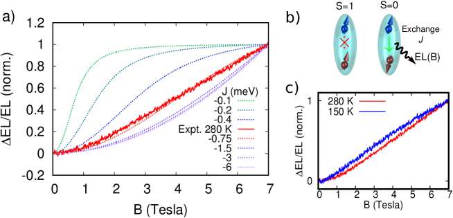
Fig. 5 shows the change in EL as a function of magnetic field calculated from Equation 2 for various values of the electron-hole exchange parameter , using =-44 meV 43; 44, 45; 46; 46, Boltzmann populations i.e., where is the electron-hole pair energy, is Boltzmann’s constant, and K is the temperature. (This population distribution assumes that electron-hole pairs thermalise within their encounter time, but due to the high temperatures involved, similar results are obtained in the fully unpolarized limit where the generation rates are equal for each spin sublevel.) We note that for which is the case we expect to apply here due to silicon’s indirect bandgap, the lineshapes are independent of and we set . This value should provide an upper bound for the internal quantum efficiency of our devices. The EQE we estimate is around 0.05%, but taking into account the reflection due to the dielectric constant mismatch at the silicon interface, an upper bound seems reasonable.
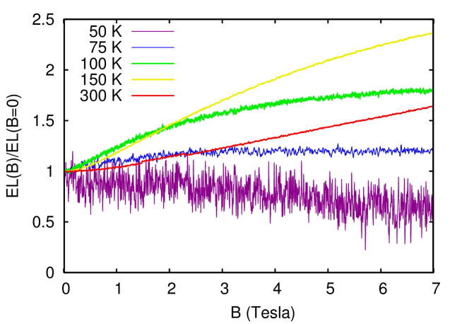
The simulations show an enhancement of the EL with magnetic field due to an increased number of states which overlap with the singlet ground state. This behavior arises from the fact that the spin-orbit interaction renormalises the effective hole -factor (with effective Landé value for total spin 3/2 holes), giving rise to a competition between the exchange interaction and the effective -factor difference (and hence Zeeman energy) between electron and hole states. This leads to a mixing between singlet and triplet electron-hole spin configurations with a characteristic saturation field set by the competition between this Zeeman energy difference and the exchange term . We find that the 300 K experimental lineshape can be reproduced with meV, which provides an estimate for typical exchange interactions for transient bound states formed during electron-hole collisions at room temperature in silicon; as expected, is smaller than the estimated exchange energy of 10 meV found for strongly bound excitonic states in Si nanocrystals 48. Highlighting the importance of transient bound pairs, we show in the Supplementary Figure 3 that the positive MEL starts to decrease below 150 K, a temperature which matches the exciton binding energy (14.7 meV). This suggests that maximal sensitivity to magnetic field is achieved when the temperature is not too high, allowing interaction effects to show up, but not too small so that electron-hole encounter events do not result in irreversible binding. We emphasise that this model produces a MEL response which does not depend on the direction of the external field, and can therefore explain the positive MEL component in our experiments (Fig. 4). While our model reproduces the observed MEL lineshapes, it fails to correctly reproduce the magnitude of the effect. The simulated value in Fig. 5 for at a magnetic field of 7 Tesla is around , as compared to the experimental . Theoretical MEL can increase up to in the limit but this would imply a very high internal quantum efficiency, which we do not believe to hold in our devices. Instead, we suggest that multiple recombination attempts, and a more detailed description of carrier kinetics as well as electron-valley mixing can further amplify the theoretical MEL magnitude. Such a complete theory is beyond the scope of this work.
In conclusion, we have reported a strong increase in the brightness of silicon LEDs under a magnetic field. These LEDs were fabricated using a novel technique which allowed us to simultaneously suppress classical magnetoresistance effects, and obtain effective emission. In analogy with magneto-optic models developed for organic semiconductors, we explained our results as arising from the difference in recombination rates between singlet and triplet electron-hole pairs, allowing the electron-hole pair exchange energy to be estimated from the experimental lineshapes. Our investigations suggest an optoelectronic approach to probe spin transport properties in silicon near room temperature, a material with promise for quantum information processing and spintronics. They also show that the control of spin properties can allow to substantially increase the brightness of SiLEDs which can be important components for chip to chip optical communication.
Acknowledgments We thank M. Entin, L. Magaril, A. Rowe and T. Chanelière for fruitful discussions and acknowledge support from PICS-Royal society, Labex ANR-10-LABX-0039-PALM, and ANR SPINEX.
Author contributions: All authors contributed to all aspects of this work.
Methods
Gas immersion Laser doping: The out-of-equilibrium laser doping was performed in ultra high vacuum (10-9 mbar) with a XeCl 308 nm excimer laser of pulse duration 25 ns and energy 0.96 J/cm2. The precursor gas used for the B(P) doping is . The doping level is finely controlled by the number of laser shots, each shot introducing a fixed B dose corresponding to the surface density of chemisorbtion sites for the precursor gas on the Si surface. The vertical alignment of the n and p doped spots is performed by illuminating the substrate from the bottom and observing the sample with an infrared camera, thus visualising the bottom spot when doping the top one.
Magneto-electroluminescence: For magneto-electruminescence experiments the samples were mounted inside an optically accessible cryostat magnet providing a static magnetic field up to 7 Tesla. The samples were thermalised at the measurement temperature through a Helium vapor. The electroluminescence was collimated outside the cryostat and focussed on a commercial Silicon or Germanium photodetector a meter away from the cryostat. Taking into account the higher sensitivity of Germanium photodetectors at the silicon emission wavelength the same results were obtained with the two types of photodetectors.
References
- (1) M.I. Dyakonov (Ed.), Spin Physics in semiconductors Springer (2008) ISBN 978-3-540-78819-5,
- (2) R. Jansen, Silicon spintronics, Nature Materials, 11(5), 400-408. (2012)
- (3) Y. Sun, N.C. Giebink, H. Kanno, B. Ma, M.E. Thompson and S.R. Forrest, Management of singlet and triplet excitons for efficient white organic light-emitting devices, Nature 440, 908 (2006)
- (4) D.D. Awschalom and M.E. Flatte, Challenges for semiconductor spintronics, Nature Physics 3, 153 (2007)
- (5) R. Schirhagl, K. Chang, M. Loretz and C.L. Degen, Nitrogen-vacancy centers in diamond: nanoscale sensors for physics and biology, Annu. Rev. Phys. Chem 65, 83 (2014)
- (6) M. Nawrocki, Yu. G. Rubo, J.P. Lascaray and D. Coquillat Suppression of the Auger recombination due to spin polarization of excess carriers and Mn 2+ ions in the semimagnetic semiconductor , Phys. Rev. B(R) 52, 2241 (1995)
- (7) D.J. Lepine Spin-dependent recombination on silicon surface, Phys. Rev. B 6, 436 (1972)
- (8) T.D. Nguyen, E. Ehrenfreund1 and Z.V. Vardeny, Spin-polarized light-emitting diode based on an organic bipolar spin valve, Science 337, 204 (2012)
- (9) J. Shinar, Optically detected magnetic resonance studies of luminescence‐quenching processes in ‐conjugated materials and organic light‐emitting devices., Laser, Photonics Reviews, 6(6), 767 (2012)
- (10) J. Wang, A.D. Chepelianskii, F. Gao, N.C. Greenham, Control of exciton spin statistics through spin polarization in organic optoelectronic devices Nature Comm. 3, 1191 (2012)
- (11) T. D. Nguyen, G. Hukic-Markosian, F. Wang, L. Wojcik, X.G. Li, E. Ehrenfreund, and Z.V. Vardeny, Isotope effect in spin response of [pi]-conjugated polymer films and devices, Nature materials 9(4), 345 (2010).
- (12) S. P. Kersten, A. J. Schellekens, B. Koopmans and P. A. Bobbert, Magnetic-field dependence of the electroluminescence of organic light-emitting diodes: a competition between exciton formation and spin mixing Phys. Rev. Lett. 106, 197402 (2011)
- (13) F. Wang, F. Macià, M. Wohlgenannt, A.D. Kent and M.E. Flatté, Phys. Rev. X, 2, 021013 (2012)
- (14) Q. Zhang, B. Li, S. Huang, H. Nomura, H. Tanaka and C. Adachi, Efficient blue organic light-emitting diodes employing thermally activated delayed fluorescence Nature Photonics 8, 326 (2014)
- (15) Wai Lek Ng, M. A. Lourenc, R. M. Gwilliam, S. Ledain, G. Shao and K. P. Homewood, An efficient room-temperature silicon-based light-emitting diode Nature 410, 192 (2001)
- (16) M.A. Green, J. Zhao, A. Wang, P.J. Reece and M. Gal, Efficient silicon light-emitting diodes Nature 412, 805 (2001)
- (17) S. Saito, F.Y. Gardes, A.Z. Al-Attili, K. Tani, K. Oda, Y. Suwa, T. Ido, Y. Ishikawa, S. Kako, S. Iwakomo and Y. Arakawa (2015). Group IV light sources to enable the convergence of photonics and electronics, Frontiers in materials 1, 66 (2014) doi:10.3389/fmats.2014.00015
- (18) M.P. Delmo, S. Yamamoto, S. Kasai, T. Ono and K. Kobayashi, Large positive magnetoresistive effect in silicon induced by the space-charge effect Nature 457, 1112 (2009)
- (19) C. Wan, X. Zhang, X. Gao, J. Wang and X. Tan, Geometrical enhancement of low-field magnetoresistance in silicon, Nature 477, 304 (2011), doi:10.1038/nature10375
- (20) D. Yang, F. Wang, Y. Ren, Y.Zuo, Y. Peng, S. Zhou and D. Xue, A Large Magnetoresistance Effect in p–n Junction Devices by the Space-Charge Effect Adv. Func. Mater 23, 2918-2923 (2013), 10.1002/adfm.201202695
- (21) N.A. Porter and C.H. Marrows Linear magnetoresistance in n-type silicon due to doping density fluctuations, Scientific reports 2:565, DOI: 10.1038/srep00565 (2012)
- (22) J. J. H. M. Schoonus, F. L. Bloom, W. Wagemans, H. J. M. Swagten, and B. Koopmans, Extremely large magnetoresistance in boron-doped silicon Phys. Rev. Lett. 100, 127202 (2008)
- (23) J. Boulmer, C. Guedj, D. Débarre, Incorporation of substitutional carbon in Si and SiGe by laser processing in methane and propylene Thin Solid Films 294, 137 (1997), http://dx.doi.org/10.1016/S0040-6090(96)09293-0
- (24) A. Bhaduri, T. Kociniewski, F. Fossard, J. Boulmer, D. Débarre, Optical and electrical properties of laser doped Si:B in the alloy range, Appl. Surf. Sc. 258, 9228 (2012), http://dx.doi.org/10.1016/j.apsusc.2011.10.077
- (25) K. Hoummada, F. Dahlem, T. Kociniewski, J. Boulmer, C. Dubois, G. Prudon, E. Bustarret, H. Courtois, D. Débarre, and D. Mangelinck, Absence of boron aggregates in superconducting silicon confirmed by atom probe tomography, Appl. Phys. Lett. 101, 182602 (2012). http://dx.doi.org/10.1063/1.4760261
- (26) F. Chiodi, A. D. Chepelianskii, C. Gardès, G. Hallais, D. Bouchier and D. Débarre, Laser doping for ohmic contacts in n-type Ge, Appl. Phys. Lett. 105, 242101 (2014); http://dx.doi.org/10.1063/1.4904416
- (27) A.J. Murrell, E.J.H Collart, M.A. Foad, and D. Jennings, Process interactions between low-energy ion implantation and rapid-thermal annealing for optimized ultrashallow junction formation , Journal of Vacuum Science & Technology B 18, 462 (2000), http://dx.doi.org/10.1116/1.591212
- (28) D. Kaplan, I. Solomon and N.F. Mott, Explanation of the large spin-dependent recombination effect in semiconductors, Journal de Physique Lettres, 39(4), 51-54. (1978)
- (29) R.E. merrifield, Magnetic effects on triplet exciton interactions, Pure and Appl. Chem 27, 481 (1971)
- (30) S.L. Bayliss, N.C. Greenham, R.H. Friend, H. Bouchiat and A.D. Chepelianskii, Spin-dependent recombination probed through the dielectric polarizability, Nature Comm. 6, 8534 (2015), doi: 10.1038/ncomms9534
- (31) B.E. Kane A silicon-based nuclear spin quantum computer, Nature, 393(6681), 133-137. (1998).
- (32) J.M. Elzerman, R. Hanson, L.W. Van Beveren, B. Witkamp, L.M.K. Vandersypen and L.P. Kouwenhoven Single-shot read-out of an individual electron spin in a quantum dot, Nature 430 431 (2004)
- (33) A. M. Tyryshkin, S. Tojo, J.J. L. Morton, H. Riemann, N.V. Abrosimov, P. Becker, H.-J. Pohl, T. Schenkel, M.L.W. Thewalt, K.M. Itoh and S.A. Lyon, Electron spin coherence exceeding seconds in high-purity silicon, Nature mat. 11 143 (2012)
- (34) A. Jüngel, Quasi-hydrodynamic semiconductor equations, (2001) ISBN 3-7643-6349-5 Birkhauser Verlag, Berlin
- (35) M. Ikai, S. Tokito, Y. Sakamoto, Y. Suzuki and Y. Taga, Highly efficient phosphorescence from organic light-emitting devices with an exciton-block layer, Appl. Phys. Lett., 79(2), 156 (2001)
- (36) J.A. Hagen, W. Li, A.J. Steckl and J.G. Grote, Enhanced emission efficiency in organic light-emitting diodes using deoxyribonucleic acid complex as an electron blocking layer, Appl. Phys. Lett., 88(17), 171109. (2006)
- (37) L. Tsybeskov, K. L. Moore, K. D. Hirschman, D. G. Hall and P. M. Fauchet, A Si‐based light‐emitting diode with room‐temperature electroluminescence at 1.1 eV , Appl. Phys. Lett. 69, 3411 (1996), http://dx.doi.org/10.1063/1.117276
- (38) M.-J. Chen, E.-Z. Liang, S.-W. Chang, and C.-F. Lin Model for band-edge electroluminescence from metal–oxide–semiconductor silicon tunneling diodes, Jour. of Appl. Phys. 90 789 (2001), http://dx.doi.org/10.1063/1.1381000
- (39) C.-F. Lin, C. W. Liu, M.-J. Chen, M. H. Lee and I. C. Lin, Electroluminescence at Si band gap energy based on metal–oxide–silicon structures, Journal of Applied Physics 87, 8793-8795 (2000), http://dx.doi.org/10.1063/1.373612
- (40) R.S. Popovic, Hall effect devices, (2004) ISBN 0-7503-0855-9
- (41) V.I. Stafeev Modulation of diffusion length as a new principle of operation of semiconductor devices, Sov. Phys.-Solid State 1 763 (1959)
- (42) S. Cristoloveanu The magnetodiode effect theory for the semiconductor and insulator regimes. Physica Status Solidi (a), 64,2, 683-695 (1981)
- (43) Shun, Lien, Chuang Physics of optoelectronic devices, Wiley Series (1995) ISBN 0-471-10939-8
- (44) O. Madelung, M. Schulz and H. Weiss, Landolt-Börnstein, Vol. 17: Semiconductors Springer (1982) ISBN 3-340-10610-3
- (45) F. A. Zwanenburg, C.E. van Rijmenam, Y. Fang, C.M. Lieber and L.P. Kouwenhoven Spin States of the First Four Holes in a Silicon Nanowire Quantum Dot , Nano letters, 9(3), 1071. (2009), DOI: 10.1021/nl803440s
- (46) B. Voisin, R. Maurand, S. Barraud, M. Vinet, X. Jehl, M. Sanquer and S. De Franceschi Electrical control of g-factor in a few-hole silicon nanowire MOSFET, Nano letters, 16(1), 88-92. (2015), DOI: 10.1021/acs.nanolett.5b02920
- (47) N.J. Harmon and M.E. Flatté, Spin relaxation in materials lacking coherent charge transport, Phys. Rev. B 90, 115203 (2014),
- (48) M. L. Brongersma, P.G. Kik, A. Polman, K.S. Min and H.A. Atwater, Size-dependent electron-hole exchange interaction in Si nanocrystals, Appl. Phys. Lett. 76, 351 (2000), http://dx.doi.org/10.1063/1.125751
- (49) P. Li and H. Dery, Theory of spin-dependent phonon-assisted optical transitions in silicon, Phys. Rev. Lett. 105, 037204 (2010)
- (50) N. Sircar and D. Bougeard, Experimental investigation of the optical spin-selection rules in bulk Si and Ge/Si quantum dots, Phys. Rev. B 89, 041301(R) (2014)
- (51) B.T. Jonker, G. Kioseoglou, A.T. Hanbicki, C.H. Li and P.E. Thompson, Electrical spin-injection into silicon from a ferromagnetic metal/tunnel barrier contact, Nature Physics, 3(8), 542 (2007)
Supplementary Information
Supplementary figure S1
Supplementary Figure S2
Supplementary Figure S3
.
Supplementary Figure S4
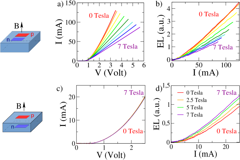
Panels c) and d) show the magnetic field effect at room temperature in vertical devices for perpendicular magnetic field for a vertical device with doping. As for the doping device shown in the main text the magnetoresistance vanishes as the curve is not changed by magnetic field (panel c) but a substantial increase in EL is observed in panel d) as opposed to the negative MEL in lateral geometry devices (panel b) .
Supplementary Figure S5
 |
Supplementary Figure S6
 |
Supplementary note 1, theoretical charge density profiles in unbiased devices
To compute the charge distribution in unbiased devices, we solve the Laplace equation on the the electrostatic potential, the dielectric permittivity, the charge of the electron:
| (S1) |
where electron density, hole density, the doping profile.
The densities , can be determined from the position of the Fermi level relative to the bottom of the conduction band and to the top of the valence band :
| (S2) | ||||
| (S3) |
In the above equation we introduced the notations and is the Fermi-integral:
| (S4) |
and , which are effective density of states in the conduction/valence bands. They are given by the following formulas 52
| (S5) | ||||
| (S6) |
which lead to and at room temperature.
Finally the electro-chemical potential remains constant across the bilayer :
| (S7) |
This leads to the following self-consistent equation on the electrostatic potential (we now count the potential from the electro-chemical potential , thus ):
| (S8) |
Boundary conditions on the electrostatic potential are given by:
| (S9) |
Choosing dimensionless units:
| (S10) |
with .
Here the potential is in units of temperature , in units of and the length-scale is set by
| (S11) |
with room temperature values for silicon:
| (S12) | ||||
| (S13) | ||||
| (S14) |
Thus we are thus finally lead to the equation:
| (S15) | ||||
| (S16) |
where all the coefficients are known ( is the complete Fermi-integral).
For , this can be integrated to:
| (S17) |
and for
| (S18) |
Combining the two conservation laws allows us to find the potential :
| (S19) |
Starting from the potential and density profiles can then be obtained by direct integration of the equations of motion.
For devices under bias the drift-diffusion equations were solved using a finite elements method.
Supplementary references :