Enhanced Superconductivity and Suppression of Charge-density Wave Order
in 2H-TaS2 in the Two-dimensional Limit
Abstract
As superconductors are thinned down to the 2D limit, their critical temperature typically decreases. Here we report the opposite behavior, a substantial enhancement of with decreasing thickness, in 2D crystalline superconductor 2H-TaS2. Remarkably, in the monolayer limit, increases to 3.4 K compared to 0.8 K in the bulk. Accompanying this trend in superconductivity, we observe suppression of the charge-density wave (CDW) transition with decreasing thickness. To explain these trends, we perform electronic structure calculations showing that a reduction of the CDW amplitude results in a substantial increase of the density of states at the Fermi energy, which contributes to the enhancement of . Our results establish ultra-thin 2H-TaS2 as an ideal platform to study the competition between CDW order and superconductivity.
pacs:
Transition metal dichalcogenides (TMDs) 2H-MX2 (where M = Nb, Ta and X = S, Se) have attracted considerable attention as intriguing 2D crystalline superconductors Saito et al. (2016a). In these materials, superconductivity (SC) forms in an environment of pre-existing charge-density wave (CDW) order Neto (2001); Kiss et al. (2007), making it an ideal platform to study many-body ground states and competing phases in the 2D limit. In bulk crystals, the reported critical temperature of the CDW transition decreases from 120 K in 2H-TaSe2 down to 30 K in 2H-NbSe2. Superconductivity weakens in approximately reverse order, with increasing from around 0.2 K in 2H-TaSe2 to 7.2 K in 2H-NbSe2. The relationship between CDW and superconductivity in such systems is still under debate Calandra et al. (2009); Ge and Liu (2012). It is generally believed that such mutual interaction is competitive, but evidence to the contrary, indicating a cooperative interaction, has also been reported in angular-resolved photoemission spectroscopy studies Kiss et al. (2007).
In TMDs, superconductivity and CDW instability can be investigated by adjusting the interlayer interactions through pressure Freitas et al. (2016); Chu et al. (1977) or molecule intercalation Thompson et al. (1972); Wilson et al. (1975). Recently, mechanical exfoliation has emerged as a robust method for producing ultra-clean, highly crystalline samples with atomic thickness Geim and Novoselov (2007). This offers a useful way to assess the effect of dimensionality and interlayer interactions on superconductivity and CDW. A material whose behavior as a function of layer thickness has been recently studied is 2H-NbSe2 Cao et al. (2015); Xi et al. (2016); Tsen et al. (2016), in which the superconducting state is progressively weaker in thinner samples, with reduced from 7 K in bulk crystals to 3 K in the monolayer. The thickness dependence of CDW order is still under debate, considering discrepancies between Raman and scanning tunneling microscopy/spectroscopy (STM/STS) studies Xi et al. (2015); Ugeda et al. (2016).
Bulk 2H-TaS2, another member of the 2H-MX2 family, exhibits a CDW transition at 70 K and a SC transition at 0.8 K Nagata et al. (1992); Neto (2001); Guillamón et al. (2011); Navarro-Moratalla et al. (2016). Compared to 2H-NbSe2, 2H-TaS2 manifests a stronger signature of CDW transition in transport in the form of a sharp decrease of resistivity Wilson et al. (1975), and thus serves as a desirable platform to study the thickness dependence of CDW instability. STM/STS measurements on monolayer TaS2 epitaxially grown on Au(111) substrates show suppression of the CDW instability Sanders et al. (2016). Recently, a study observed an enhanced down to a thickness of 3.5 nm, utilizing TaS2 flakes directly exfoliated on a Si/SiO2 substrate Navarro-Moratalla et al. (2016). Unfortunately, it was found that samples thinner than that become insulating, indicative of its particular susceptibility to degradation in ambient atmosphere. Therefore, exfoliation and encapsulation in an inert atmosphere become crucial to attain high quality samples.
Here we report that superconductivity persists in 2H-TaS2 down to the monolayer limit, with a pronounced increase in from 0.8 K in bulk crystals to 3.4 K in the monolayer. Two transport observations, that in the bulk signal the CDW transition, are found to vanish in ultra-thin samples: (1) a kink in the temperature dependence of the resistivity, and (2) a change of sign in the Hall coefficient versus temperature. In search of an origin for such trends, we perform electronic structure and phonon spectrum calculations. We show that suppression of the CDW order leads to a substantial increase in the density of states at the Fermi level, , which ultimately enhances . Our observations also motivates consideration of quantum fluctuations of the CDW order as another mechanism that boosts . This provides new insights into the impact of reduced dimensions on many-body ground states and their interactions.
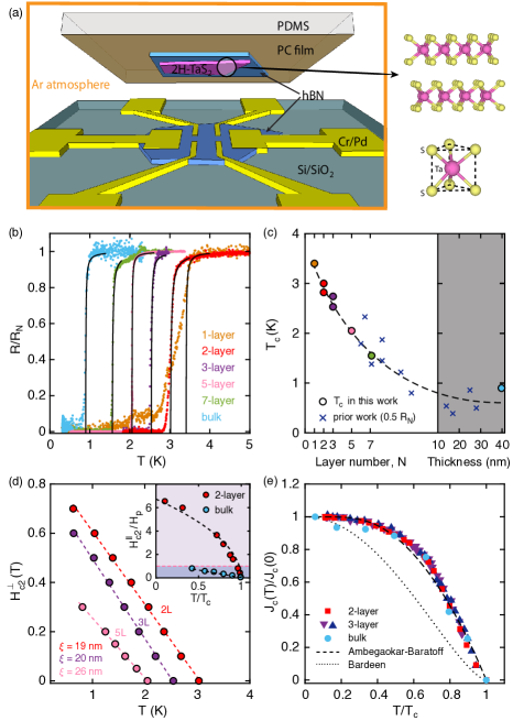
In this work, we exfoliate and fabricate samples with a transfer set-up built inside a glove box filled with Argon gas, and encapsulate the TaS2 flake between two sheets of hexagonal boron nitride SM . We build our devices utilizing a polymer pick-up technique Wang et al. (2015) as illustrated in Fig. 1 (a), taking advantage of the van der Waals adhesion between 2D layers. With this method, we are able to obtain high quality few-layer TaS2 devices. As seen in Fig. 1 (b), when temperature is sufficiently low, a clear superconducting transition is observed for 1, 2, 3, 5, 7-layer, and bulk samples. By fitting the resistance to the Aslamazov-Larkin expression Aslamasov and Larkin (1968), we are able to determine the mean-field superconducting transition temperature . When sample thickness is decreased from bulk to monolayer, the corresponding monotonically increases from 0.9 K to 3.4 K 111For the monolayer flake, determination of becomes tricky due to electrical shortage to adjacent flakes with different thickness. Detailed analysis and determination of by critical current mapping can be found in Supplemental Material SM .. The trend observed in our experiment is strictly opposite that of a previous finding on 2H-NbSe2 Xi et al. (2016), where decreases monotonically with thickness reduction, despite the fact that the two materials are isostructural and isovalent. In 2H-NbSe2, the decreased is attributed to a weaker interlayer Cooper pairing given by cos as layer number is reduced. In our case, however, it is surprising to see that even with a reduced interlayer Cooper pairing, the is dramatically enhanced. To verify that the thickness dependence of is independent of extrinsic factors (such as level of disorder, substrate, source of crystal, sample quality), we measure an additional set of bilayer and trilayer samples and plot our results alongside previously reported values Navarro-Moratalla et al. (2016) in Fig. 1 (c). Regardless of different sample preparation procedures and substrates, the trend of versus thickness is consistent between the two sets of experimental results, indicative of an intrinsic origin underlying the enhancement of .
To further characterize the superconducting properties of thin TaS2, we characterize the superconducting transition under both out-of-plane and in-plane magnetic fields. Fig. 1 (d) shows the as a function of temperature. Close to , the dependence of is fitted well by the phenomenological 2D Ginzburg-Landau (GL) model, which yields nm for 2, 3, 5-layer respectively, where denotes the GL coherence length at zero temperature. The reported value for 3D ranges from 22 nm Kashihara et al. (1979) to 32.6 nm Abdel-Hafiez et al. (2016). For in-plane field, we observe a much larger T at 300 mK for a bilayer ( K), which is more than six times the Pauli paramagnetic limit , obeying a square root rather than a linear temperature dependence (inset of Fig. 1 (d)). This dramatic enhancement of in-plane , often referred to as Ising superconductivity, has been observed in other 2D crystalline superconductors Lu et al. (2015); Saito et al. (2016b); Xi et al. (2016); Tsen et al. (2016). The above observations verify that thin TaS2 behaves as a 2D superconductor. We also show that the superconducting transition also exhibits the Berezinskii-Kosterlitz-Thouless (BKT) transition as expected in 2D in the Supplemental Material SM . Additionally, the critical current density increases by orders of magnitude as the devices become thinner (bulk A/cm2, trilayer A/cm2, bilayer A/cm2). The trend of critical current density versus temperature for representative thicknesses is shown in Fig. 1 (e), with a more detailed discussion in Supplemental Material SM .
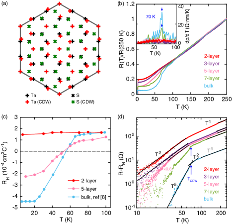
In addition to SC transition, bulk 2H-TaS2 is known to manifest CDW order below 70 K. Fig. 2 (a) illustrates the atomic displacements in the CDW state for monolayer. Two well established indicators of the CDW phase in bulk TaS2 are a kink in the resistivity occurring at = 70 K and a change of sign in the Hall coefficient as the temperature is reduced below . We find that both disappear as the sample thickness is reduced towards the 2D limit. Shown in Fig. 2 (b) is a plot of normalized resistance versus temperature on a linear scale. All samples manifest a linear decrease of resistance at high temperatures, consistent with phonon limited resistivity in a normal metal El-Bana et al. (2013). Below 70 K, the 7-layer and bulk devices undergo a CDW phase transition, producing a sudden drop in resistance. This is confirmed by calculating the temperature derivative of the resistivity, as shown in the inset of Fig. 2 (b). A peak in develops close to the transition. In 2, 3, 5-layer, however, such a sudden drop is not noticeable.
The Hall effect has been used to verify the existence of a phase transition. The Hall coefficient is found to demonstrate a broad transition between 70 and 20 K and a change in sign at 56 K in bulk crystals Thompson et al. (1972). This indicates that the CDW transition not only induces a structural change, but also alters the electronic properties of the material. It has been shown that a two-carrier model with light holes and heavy electrons is necessary to explain the opposite signs for the Seebeck and Hall coefficients measured above the CDW transition temperature; a single-carrier model describes the low-temperature behavior Thompson et al. (1972). In Fig. 2 (c), we plot the Hall coefficient of three representative thicknesses below 100 K. In the 5-layer device, a significant deviation from the bulk behavior is already apparent: the overall magnitude of and temperature where it switches sign, are both diminished. However, the most striking fact is the weak temperature dependence and absence of a sign change in the 2-layer sample. This provides unambiguous evidence that the CDW transition occurring in bulk samples is absent in the ultra-thin limit.
Another interesting observation is the emergence of behavior in ultra-thin samples. In Fig. 2 (d), we plot the subtracted resistance on a log-log scale. For bulk, the linear temperature dependence is disrupted by a sudden switch to near . has been well known as a consequence of electron-phonon scattering at temperatures lower than the Debye temperature . In contrast, a gradual transition to is observed in 2, 3-layer; it persist from 55 K down to the onset temperature of superconductivity. Naively, such behavior results from electron-electron scattering within Fermi liquid theory. However, we find that the observed coefficient is too large to be explained within such a framework. Moreover, assuming the e-e scattering strength is not greatly altered from 3D to 2D SM , it is implausible that the behavior is completely absent in thick samples in the same temperature range. Here we propose an alternative mechanism that leads to a resistivity: scattering of electrons by soft phonons, i.e. critical CDW fluctuations, which can happen close to a finite momentum ordering transition Hlubina and Rice (1995) (see Supplemental Material SM ). This picture is motivated by the longitudinal and Hall resistivity data indicating the disappearance of the CDW order in thin samples. It assumes that although the long range CDW order has been destroyed, strong CDW fluctuations remain, which can scatter electrons.
It is worth noting that a similar anti-correlation of trends of SC and CDW transition has also been observed in 2H-TaS2 crystals under pressure Freitas et al. (2016); Abdel-Hafiez et al. (2016) and single crystal alloys Wagner et al. (2008); Fang et al. (2016); Li et al. (2017). To better understand the connection between CDW and superconductivity, we recall that in McMillan’s theory, the critical temperature is expressed as McMillan (1968)
| (1) |
where is the Coulomb pseudopotential of Morel and Anderson, and is the electron-phonon coupling constant. Assuming as suggested by McMillan McMillan (1968), one can evaluate the inverted form of Eq. (1) and obtain for TaS2 with K Schlicht et al. (2001) and K Navarro-Moratalla et al. (2016), indicating that TaS2 lies in the intermediate coupling regime.
The CDW instability allows electronic systems to lower their energy by inducing energy gaps in the spectrum. Since can affect both and , it plays an important role in determining . We investigate the electronic and vibrational properties of 2H-TaS2 based on density functional theory (DFT). First, we implemented in VASP code Kresse and Furthmüller (1996a, b) in order to obtain the DOS in the normal and the CDW phases for monolayer, bilayer and bulk. A comparison of Fig. 3 (b) and (c) reveals an appreciable reduction of DOS near the Fermi level induced by CDW order for all three thicknesses. This is consistent with previous magnetic susceptibility and heat capacity experiments showing a sharp drop of density of states below the CDW transition Di Salvo et al. (1971); Mattheiss (1973). Further, to visualize the effects of CDW on the pristine band structure, we derive the unfolded band structure in the CDW phase, shown in Fig. 3 (a), based on the Fourier decompositions of the Bloch wavefunctions from the tight-binding Hamiltonians Farjam (2015); Popescu and Zunger (2012) (see Supplemental Material SM ). It is clearly seen that a band gap, , emerges in the inner pocket around K along -K and K-M. In addition, the saddle point located along the -K, is shifted to energies above the Fermi level. Next, we compute the phonon dispersion for the bulk and monolayer (see Supplemental Material SM ). In both the bulk and monolayer, an acoustic mode that involves in-plane motion of Ta atoms softens and becomes unstable as the electronic temperature is lowered. We found that in both cases the instability occurs at approximately the same wave vector that corresponds to the CDW ordering M Albertini et al. (2017).
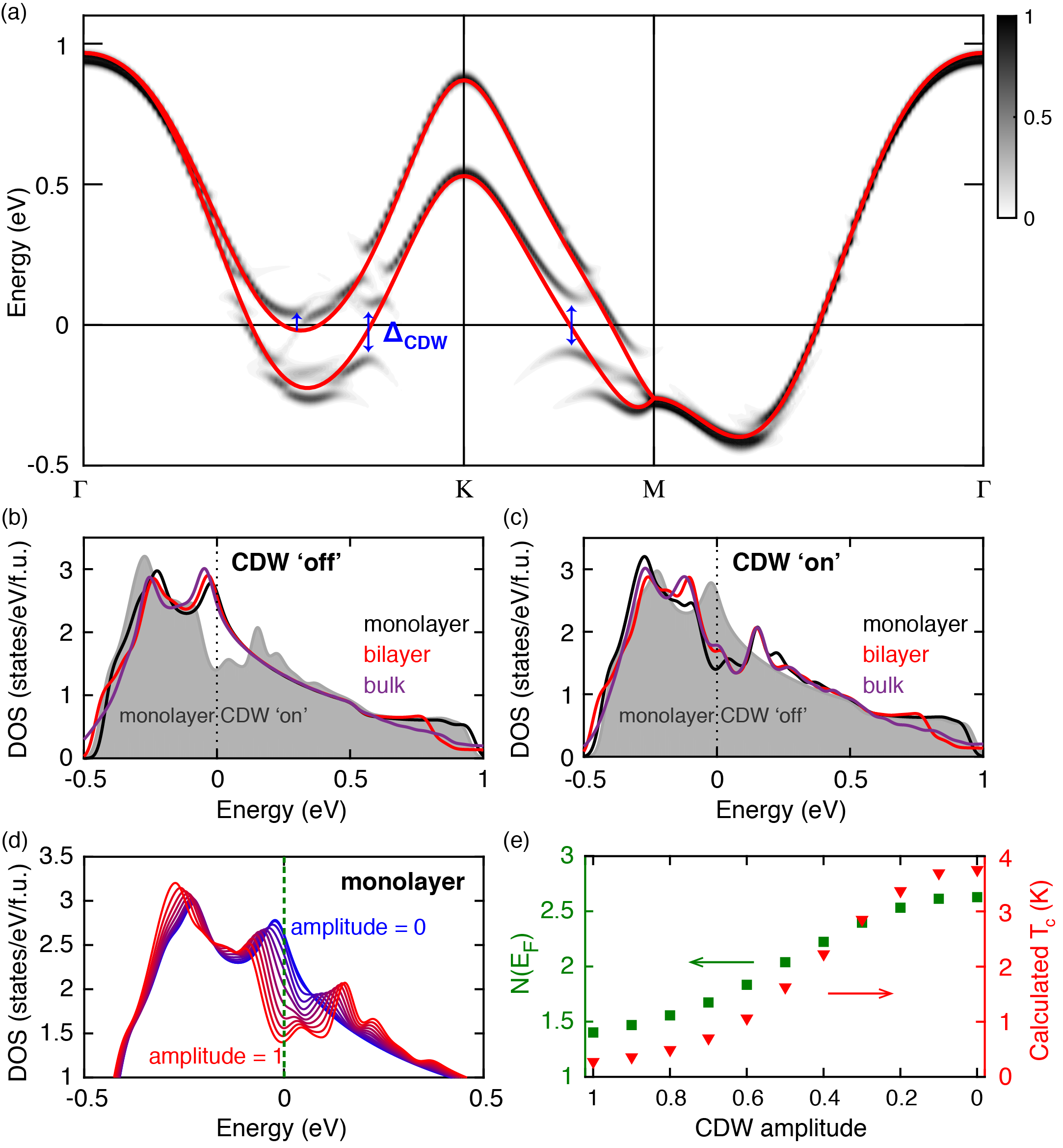
We then investigate the impact of progressive weakening of the CDW with decreasing thickness by varying the magnitude of atomic distortion. A scaling factor, from 1 to 0, is used to define the fraction by which the magnitude of the atomic displacement is reduced with respect to the stable distorted configuration. The corresponding DOS as a function of atom displacement amplitude is calculated and plotted in Fig. 3 (d). Using the bulk as a starting point, we take into account the change in and a small phonon energy shift calculated for monolayer, and plot the predicted within the McMillan formalism in Fig. 3 (e). An enhancement of up to 3.75 K is achieved when the amplitude of CDW goes to zero. This gives a rough estimate of the impact of the suppression of the CDW order on the superconducting , which leads to a reasonable prediction that aligns with the experimental value. We note that it is not entirely clear that the enhancement of is solely due to the enhanced DOS. There are several factors impacting that have been discussed previously but not addressed in our calculation, such as substrate effects, the presence of a van Hove singularity near the Fermi level and enhanced electron-phonon coupling due to reduced screening in two dimensions Navarro-Moratalla et al. (2016), and a weaker interlayer Cooper pairing Xi et al. (2016).
This is not the first experiment indicating that a CDW phase transition vanishes in reduced dimensions Thompson et al. (1972); Ayari et al. (2007); Pan et al. (2017); Sanders et al. (2016); Yoshida et al. (2015). Its origin is still under debate Ayari et al. (2007); Ge and Liu (2012). Recently, a study showed that lattice fluctuations arising from the strong electron-phonon coupling act to suppress the onset temperature of CDW order, leading to a pseudogap phase characterized by local order and strong phase fluctuations Flicker and van Wezel (2016). This is consistent with our model of presence of soft phonons, or CDW fluctuations Naito and Tanaka (1982) as primary contributor to the behavior of resistivity observed above . More interestingly, theory predicts that quantum fluctuations caused by proximity to a CDW transition can boost superconducting pairing by providing sources of bosonic excitations Wang and Chubukov (2015). Although there is no direct evidence that CDW fluctuations facilitate superconductivity in 2H-TaS2, this scenario reveals a potentially rich relationship between CDW and SC.
In conclusion, we observe enhanced superconductivity in atomically thin 2H-TaS2 accompanied with suppression of the CDW order.
Our electronic band structure calculation shows that suppression of the CDW phase leads to a substantial increase in , which acts to boost the superconducting .
We further suggest that the emergence of behavior in ultra-thin samples is attributable to the scattering of electrons with soft phonon modes, indicative of critical CDW fluctuations.
Future studies of the layer dependence of the CDW order, for example, STM/STS and ultrafast spectroscopy studies, will be essential to understanding both the origin of the CDW and the relationship between CDW and superconductivity.
Acknowledgements.
We thank Yuan Cao, Jason Luo and Jiarui Li for experimental help. We also thank Patrick A. Lee, Dennis Huang, Miguel A. Cazalilla and Bertrand I. Halperin for fruitful discussions. This work has been primarily supported by the US DOE, BES Office, Division of Materials Sciences and Engineering under Award DE-SC0001819 (YY and PJH) and by the Gordon and Betty Moore Foundation s EPiQS Initiative through Grant GBMF4541 to PJH Fabrication work (ENM) and theory analysis were partly supported by the NSF-STC Center for Integrated Quantum Materials under award No. DMR-1231319 (VF, SF) and ARO MURI Award W911NF-14-0247 (EK). This work made use of the MRSEC Shared Experimental Facilities supported by NSF under award No. DMR-0819762 and of Harvard s CNS, supported by NSF under Grant ECS-0335765. SF used Odyssey cluster of the FAS by the Research Computing Group at Harvard University, and the Extreme Science and Engineering Discovery Environment, which is supported by NSF Grant No. ACI-1053575. JR acknowledges the Gordon and Betty Moore Foundation under the EPiQS initiative under Grant No. GBMF4303. A portion of this work was performed at the National High Magnetic Field Laboratory, which is supported by NSF Cooperative Agreement No. DMR-1157490 and the State of Florida. Growth of hexagonal boron nitride crystals was supported by the Elemental Strategy Initiative conducted by the MEXT, Japan and JSPS KAKENHI Grant Numbers JP15K21722 and JP25106006.References
- Saito et al. (2016a) Y. Saito, T. Nojima, and Y. Iwasa, Nat. Rev. Mater. 2 (2016a).
- Neto (2001) A. C. Neto, Phys. Rev. Lett. 86, 4382 (2001).
- Kiss et al. (2007) T. Kiss, T. Yokoya, A. Chainani, S. Shin, T. Hanaguri, M. Nohara, and H. Takagi, Nat. Phys. 3, 720 (2007).
- Calandra et al. (2009) M. Calandra, I. Mazin, and F. Mauri, Phys. Rev. B 80, 241108 (2009).
- Ge and Liu (2012) Y. Ge and A. Y. Liu, Phys. Rev. B 86, 104101 (2012).
- Freitas et al. (2016) D. Freitas, P. Rodiere, M. Osorio, E. Navarro-Moratalla, N. Nemes, V. Tissen, L. Cario, E. Coronado, M. García-Hernández, S. Vieira, et al., Phys. Rev. B 93, 184512 (2016).
- Chu et al. (1977) C. Chu, V. Diatschenko, C. Huang, and F. DiSalvo, Phys. Rev. B 15, 1340 (1977).
- Thompson et al. (1972) A. Thompson, F. Gamble, and R. Koehler Jr, Phys. Rev. B 5, 2811 (1972).
- Wilson et al. (1975) J. A. Wilson, F. Di Salvo, and S. Mahajan, Adv. in Phys. 24, 117 (1975).
- Geim and Novoselov (2007) A. K. Geim and K. S. Novoselov, Nat. Mater. 6, 183 (2007).
- Cao et al. (2015) Y. Cao, A. Mishchenko, G. Yu, E. Khestanova, A. Rooney, E. Prestat, A. Kretinin, P. Blake, M. Shalom, C. Woods, et al., Nano Lett. 15, 4914 (2015).
- Xi et al. (2016) X. Xi, Z. Wang, W. Zhao, J.-H. Park, K. T. Law, H. Berger, L. Forró, J. Shan, and K. F. Mak, Nat. Phys. 12, 139 (2016).
- Tsen et al. (2016) A. W. Tsen, B. Hunt, Y. D. Kim, Z. J. Yuan, S. Jia, R. J. Cava, J. Hone, P. Kim, C. R. Dean, and A. N. Pasupathy, Nat. Phys. 12, 208 (2016).
- Xi et al. (2015) X. Xi, L. Zhao, Z. Wang, H. Berger, L. Forró, J. Shan, and K. F. Mak, Nat. Nanotechnol. 10, 765 (2015).
- Ugeda et al. (2016) M. M. Ugeda, A. J. Bradley, Y. Zhang, S. Onishi, Y. Chen, W. Ruan, C. Ojeda-Aristizabal, H. Ryu, M. T. Edmonds, H.-Z. Tsai, et al., Nat. Phys. 12, 92 (2016).
- Nagata et al. (1992) S. Nagata, T. Aochi, T. Abe, S. Ebisu, T. Hagino, Y. Seki, and K. Tsutsumi, J. Phys. Chem. Solids 53, 1259 (1992).
- Guillamón et al. (2011) I. Guillamón, H. Suderow, J. G. Rodrigo, S. Vieira, P. Rodière, L. Cario, E. Navarro-Moratalla, C. Martí-Gastaldo, and E. Coronado, New J. Phys. 13, 103020 (2011).
- Navarro-Moratalla et al. (2016) E. Navarro-Moratalla, J. O. Island, S. Mañas-Valero, E. Pinilla-Cienfuegos, A. Castellanos-Gomez, J. Quereda, G. Rubio-Bollinger, L. Chirolli, J. A. Silva-Guillén, N. Agraït, G. A. Steele, F. Guinea, H. S. J. van der Zant, and E. Coronado, Nat. Commun. 7, 11043 (2016).
- Sanders et al. (2016) C. E. Sanders, M. Dendzik, A. S. Ngankeu, A. Eich, A. Bruix, M. Bianchi, J. A. Miwa, B. Hammer, A. A. Khajetoorians, and P. Hofmann, Phys. Rev. B 94, 081404 (2016).
- Tinkham (2004) M. Tinkham, Introduction to superconductivity (Dover, New York, 2004).
- Bardeen (1962) J. Bardeen, Rev. Mod. Phys. 34, 667 (1962).
- Ambegaokar and Baratoff (1963) V. Ambegaokar and A. Baratoff, Phys. Rev. Lett. 10, 486 (1963).
- (23) See Supplemental Material for further details.
- Wang et al. (2015) J. I.-J. Wang, Y. Yang, Y.-A. Chen, K. Watanabe, T. Taniguchi, H. O. Churchill, and P. Jarillo-Herrero, Nano Lett. 15, 1898 (2015).
- Aslamasov and Larkin (1968) L. Aslamasov and A. Larkin, Phys. Lett. A 26, 238 (1968).
- Note (1) For the monolayer flake, determination of becomes tricky due to electrical shortage to adjacent flakes with different thickness. Detailed analysis and determination of by critical current mapping can be found in Supplemental Material SM .
- Kashihara et al. (1979) Y. Kashihara, A. Nishida, and H. Yoshioka, J. Phys. Soc. Jpn. 46, 1112 (1979).
- Abdel-Hafiez et al. (2016) M. Abdel-Hafiez, X.-M. Zhao, A. Kordyuk, Y.-W. Fang, B. Pan, Z. He, C.-G. Duan, J. Zhao, and X.-J. Chen, Sci. Rep. 6 (2016).
- Lu et al. (2015) J. Lu, O. Zheliuk, I. Leermakers, N. F. Yuan, U. Zeitler, K. T. Law, and J. Ye, Science 350, 1353 (2015).
- Saito et al. (2016b) Y. Saito, Y. Nakamura, M. S. Bahramy, Y. Kohama, J. Ye, Y. Kasahara, Y. Nakagawa, M. Onga, M. Tokunaga, T. Nojima, et al., Nat. Phys. 12, 144 (2016b).
- El-Bana et al. (2013) M. S. El-Bana, D. Wolverson, S. Russo, G. Balakrishnan, D. M. Paul, and S. J. Bending, Supercond. Sci. Technol. 26, 125020 (2013).
- Hlubina and Rice (1995) R. Hlubina and T. Rice, Phys. Rev. B 51, 9253 (1995).
- Wagner et al. (2008) K. E. Wagner, E. Morosan, Y. S. Hor, J. Tao, Y. Zhu, T. Sanders, T. M. McQueen, H. W. Zandbergen, A. J. Williams, D. V. West, and R. J. Cava, Phys. Rev. B 78, 104520 (2008).
- Fang et al. (2016) L. Fang, P. Y. Zou, Y. Wang, L. Tang, Z. Xu, H. Chen, C. Dong, L. Shan, and H. H. Wen, Sci. Technol. Adv. Mater. 6, 736 (2016).
- Li et al. (2017) L. Li, X. Deng, Z. Wang, Y. Liu, and M. Abeykoon, npj Quant. Mater. 2, 11 (2017).
- McMillan (1968) W. McMillan, Phys. Rev. 167, 331 (1968).
- Schlicht et al. (2001) A. Schlicht, M. Schwenker, W. Biberacher, and A. Lerf, J. Phys. Chem. B 105, 4867 (2001).
- Kresse and Furthmüller (1996a) G. Kresse and J. Furthmüller, Phys. Rev. B 54, 11169 (1996a).
- Kresse and Furthmüller (1996b) G. Kresse and J. Furthmüller, Comput. Mater. Sci. 6, 15 (1996b).
- Di Salvo et al. (1971) F. Di Salvo, R. Schwall, T. Geballe, F. Gamble, and J. Osiecki, Phys. Rev. Lett. 27, 310 (1971).
- Mattheiss (1973) L. Mattheiss, Phys. Rev. B 8, 3719 (1973).
- Farjam (2015) M. Farjam, arXiv:1504.04937 (2015).
- Popescu and Zunger (2012) V. Popescu and A. Zunger, Phys. Rev. B 85, 085201 (2012).
- Albertini et al. (2017) O. R. Albertini, A. Y. Liu, and M. Calandra, Phys. Rev. B 95, 235121 (2017).
- Ayari et al. (2007) A. Ayari, E. Cobas, O. Ogundadegbe, and M. S. Fuhrer, J. Appl. Phys. 101, 014507 (2007).
- Pan et al. (2017) J. Pan, C. Guo, C. Song, X. Lai, H. Li, W. Zhao, H. Zhang, G. Mu, K. Bu, T. Lin, X. Xie, M. Chen, and F. Huang, J. Am. Chem. Soc. 139, 4623 (2017).
- Yoshida et al. (2015) M. Yoshida, R. Suzuki, Y. Zhang, M. Nakano, and Y. Iwasa, Sci. Adv. 1, e1500606 (2015).
- Flicker and van Wezel (2016) F. Flicker and J. van Wezel, Phys. Rev. B 94, 235135 (2016).
- Naito and Tanaka (1982) M. Naito and S. Tanaka, J. Phys. Soc. Jpn. 51, 219 (1982).
- Wang and Chubukov (2015) Y. Wang and A. V. Chubukov, Phys. Rev. B 92, 125108 (2015).