Strongly anisotropic spin relaxation in graphene/transition metal dichalcogenide heterostructures at room temperature
Abstract
A large enhancement in the spin-orbit coupling of graphene has been predicted when interfacing it with semiconducting transition metal dichalcogenides. Signatures of such an enhancement have been reported but the nature of the spin relaxation in these systems remains unknown. Here, we unambiguously demonstrate anisotropic spin dynamics in bilayer heterostructures comprising graphene and tungsten or molybdenum disulphide (WS2, MoS2). We observe that the spin lifetime varies over one order of magnitude depending on the spin orientation, being largest when the spins point out of the graphene plane. This indicates that the strong spin-valley coupling in the transition metal dichalcogenide is imprinted in the bilayer and felt by the propagating spins. These findings provide a rich platform to explore coupled spin-valley phenomena and offer novel spin manipulation strategies based on spin relaxation anisotropy in two-dimensional materials.
Graphene has emerged as the foremost material for future two-dimensional spintronics due to its tuneable electronic properties han2014 ; SR2014 ; SR2015 ; SOV2017 . Spin information can be transported over long distances kamalakar2015 ; drogeler2016 and, in principle, be manipulated by using magnetic correlations or large spin-orbit coupling (SOC) induced by proximity effects SOV2017 ; marchenko2012 ; klimovskikh2014 ; avsar2014 ; gmitra2015 ; gmitra2016 ; wang2015 ; wang2016 ; yang2016 ; yang2017 ; vaklinova2016 ; dushenko2016 ; WST2017 ; garcia2017 ; offidani2017 . First principle calculations have shown that semiconducting transition metal dichalcogenides (TMDC) can induce a SOC in graphene in the meV range while preserving its linear Dirac band structure gmitra2015 ; gmitra2016 . The enhancement of the SOC has been demonstrated using non-local charge transport and weak (anti-)localization measurements avsar2014 ; wang2015 ; wang2016 ; yang2016 ; yang2017 , the most salient signature being a drastic reduction of the spin lifetime down to the picosecond range. In recent spin transport experiments, the spin sink effect in TMDCs was used to modulate the transmission of pure spin currents. This enabled the realization of a spin field-effect switch that changes between “on” and “off” by gate tuning yan2016 ; dankert2017 .
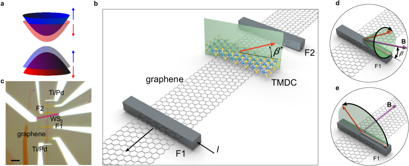
A further consequence of the proximity-induced SOC by a TMDC, which has not been addressed experimentally, is the imprint of the strong spin-valley coupling wang2012 ; xiao2012 ; yang2015 ; ye2016 ; rivera2016 . As depicted in Fig. 1a, a band gap should open in the graphene Dirac cone due to the breaking of pseudospin symmetry, while the SOC, combined with broken space inversion symmetry, removes the spin degeneracy gmitra2015 ; gmitra2016 . The spins in these bands tilt out of the graphene plane, with the out-of-plane component alternating from up to down as the energy of the bands increases, in a sequence that inverts between the and points of the Brillouin zone.
The spin splitting and texture in graphene/TMDC imply that the spin dynamics would likely differ for spins pointing in () and out of () the graphene plane, leading to distinct spin lifetimes, and , and associated spin relaxation lengths, and . Indeed, realistic modelling predicts that the spin lifetime anisotropy ratio could reach values as large as a few hundreds, in the presence of intervalley scattering cummings2017 . Quantification of can therefore provide unique insight into spin-valley coupling mechanisms and help elucidate the nature of the induced SOC in graphene han2014 ; BR2016 .
Recent experiments have demonstrated that can be determined combining in-plane and out-of plane spin precession measurements BR2016 ; BR2017 . In order to reveal the nature of the spin dynamics in graphene/TMDC, we implement such a technique using the device depicted in Fig. 1b, with TMDC being either WS2 or MoS2. The experiments are based on the standard non-local spin injection and detection approach js1985 ; jedema2001 ; SOV2009 . A multilayer TMDC flake is placed over graphene between the ferromagnetic injector (F1) and detector (F2) electrodes, creating a graphene/TMDC van der Walls heterostructure (see Methods and Fig. 1c). The TMDC modifies the graphene band structure by proximity effect and, as a consequence, the spin relaxation. Considering that in the modified graphene region is expected to be in the range of a few ps dankert2017 ; cummings2017 , the spin relaxation length should be in the submicron range. The width of the TMDC flake is thus selected to be about one micrometre so as not to completely suppress the spin population when spins are in-plane. The spin channel length , which is defined as the distance between F1 and F2, is much longer than (about 10 m) to ensure that the spin precession can be studied at moderate magnetic fields BR2016 ; BR2017 . A back-gate voltage is applied to the substrate to tune the spin absorption in the TMDC yan2016 ; dankert2017 while all the measurements are acquired at room temperature.
Owing to magnetic shape anisotropy, the magnetizations of F1 and F2 tend to be in-plane. A perpendicular magnetic field causes spins to precess exclusively in plane and senses only. In order to obtain , the strategies represented in Figs. 1d and 1e are followed. These strategies are described in Refs. BR2016 ; BR2017 and rely on the application of an oblique characterized by an angle (Fig. 1d) or an in-plane perpendicular to the easy magnetization axes of F1/F2 (Fig. 1e). As represented by the red arrows, such magnetic fields force the spins to precess out of the plane as they diffuse towards the detector. When a spin reaches the graphene/TMDC region, its orientation relative to the graphene plane is characterized by the angle , which depends on the magnitude of (Fig. 1b). The spin precession dynamics therefore becomes sensitive to both and , and can be determined.
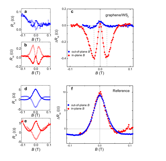
Figure 2 demonstrates the changes in the spin precession lineshape, vs , induced by the TMDC. The non-local spin resistance is determined from the voltage at the detector F2, which is generated by a current flowing at the injector F1 (Fig. 1b). Figures 2a to 2c show measurements for a typical graphene/WS2 device (Device 1). The data are acquired for parallel and antiparallel configurations of the F1/F2 magnetizations. Figures 2d to 2f show equivalent measurements for a reference device (without WS2), which was fabricated in the same graphene flake (Fig. 1c).
The spin precession response in the two devices is strikingly different. Figures 2a and 2d present conventional spin precession measurements with an out-of-plane magnetic field. Even though spin precession is observed in both cases, in the graphene/WS2 device (Fig. 2a) is two orders of magnitude smaller than in the reference (Fig. 2d). The decrease in indicates a large reduction of in the graphene/WS2 region, as observed previously for MoS2 dankert2017 . The value of can be determined by solving the diffusive equations at (Supplementary Information). From the change in between the graphene/WS2 and the reference devices, is estimated to be about 0.2-0.4 m, which is significantly smaller than the typical 3-5 m in our pristine graphene.
Figures 2b and 2e present spin precession measurements for in-plane , as shown in Fig. 1e. While the change in the orientation results in no significant variation in the reference device, the changes observed in the graphene/WS2 device are remarkable (compare Figs. 2a and 2b). Figure 2b shows that, as increases, becomes much larger than its value at . The anomalous enhancement of is a clear indication of anisotropic spin relaxation, with larger than and thus . Similar results for three other devices are shown in Supplementary Fig. 1, one of them with MoS2, which demonstrates that the anisotropic relaxation is not limited to graphene/WS2.
The difference between Figs. 2d and 2e is due to the tilting of the F1/F2 magnetizations with . The tilting angle , which is calculated from the fittings to the spin precession in the reference BR2016 , is more pronounced for in-plane , for which the shape anisotropy is smaller. In an isotropic system, the non-local resistance has the form for initially parallel (+) and antiparallel (-) magnetization configurations, with a function that captures the precession response BR2017 ; jedema2001 ; SOV2009 . By defining , it is evident that, for an isotropic system and small , is independent of the orientation. The obtained for in-plane (red) and out-of-plane (blue) are shown in Figs. 2c and 2f for the graphene/WS2 and the reference device, respectively. The nearly perfect overlap of the two curves in Fig. 2f is a consequence of the isotropic spin relaxation in graphene BR2016 ; BR2017 while the disparity of the curves in Fig. 2c further demonstrates the highly anisotropic nature of the spin transport in graphene/WS2. The extrema in are reached when the aggregate orientation of the diffusing spins have rotated by at the WS2 location. Because the diffusing spins pass by WS2 before F2, this occurs at magnetic fields that are slightly larger than those at which in the conventional spin precession measurements (dashed vertical lines in Fig. 2c).
Having determined , can be obtained using out-of-plane precession with oblique . Because the spins diffuse towards WS2, they are characterized by a broad distribution of inclination angles (Fig. 1b). As increases, the spin component that is perpendicular to the magnetic field dephases and only the component parallel to contributes to BR2016 . In the case depicted in Fig. 1d, this component is non-zero and the spin orientation is univocally determined by , which greatly simplifies the analysis to obtain and . Indeed, the effective spin relaxation length in graphene/WS2 for arbitrary , , can be calculated using the same procedure that is used to find (Supplementary Information). Note that, to achieve full dephasing at moderate , the WS2 flake is close to the ferromagnetic electrode that typically plays the role of detector (F2 in Fig. 1b).
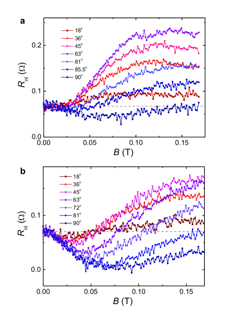
Figure 3a shows spin precession measurements for a representative set of values for Device 2, with F2 as detector. A back-gate voltage V is applied to suppress the spin absorption in WS2 (see below). It is observed that diffusive broadening dephases the precessional motion at T. For , is nearly constant with increasing , with a magnitude . At , the response is similar to that in Fig. 2a. However, as soon as is tilted from the perpendicular orientation, increases anomalously, and a few degrees tilt results in even at small (e.g. for ). This is in stark contrast to the case of pristine graphene. Equivalent measurements for a reference device are shown in Supplementary Fig. 2; there and is an upper limit for BR2016 . As a comparison, Fig. 3b shows measurements with the role of F1 and F2 reversed. Because the injector (F2) is now close to WS2, the aggregate spin precession angle at the WS2 location for any given , is smaller than in the case where the injector is far away (Fig. 3a). Full dephasing at graphene/WS2 is not achieved, while does not reach the largest values observed in Fig. 3a, which implies that the spins do not fully rotate out of plane.
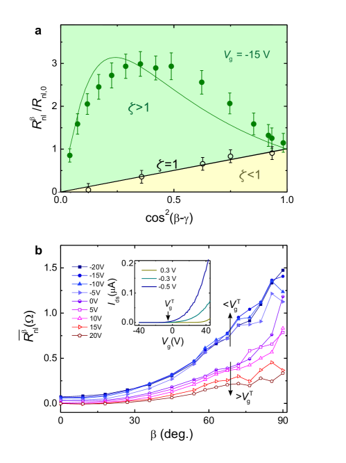
For a generic anisotropic spin channel, can be written as , where is the non-local resistance that would be measured if the magnetization of the injector and detector were parallel to . The factor thus accounts for the projection of the injected spins along and the subsequent projection along the detector magnetization BR2016 . For , regardless of the value of ; therefore, plotting versus results in a straight line. For , lies above or below the straight line depending whether or BR2016 . The magnitude of normalized to is shown in Fig. 4a both for the graphene/WS2 and the reference devices (full and open symbols, respectively), as extracted from Fig. 3a and Supplementary Fig. 2. Consistent with the results in Fig. 2, for the reference, while for graphene/WS2.
In order to find the origin of the anisotropy, the spin transport is studied as a function of , which tunes the carrier density of both graphene and WS2. Figure 4b shows the obtained vs. for different . Below a threshold back-gate voltage V, is nearly independent of . However, for , a rapid reduction of is observed for all values of . For V, no spin signal can be detected when the spins are oriented in-plane; the spin signal is recovered as soon as the out-of-plane spin component is non zero, indicating that for all values of . A vanishing for positive has been recently reported in graphene/MoS2 heterostructures and was attributed to the change of the MoS2 channel conductivity and associated modulation of the Schottky barrier at the MoS2/graphene interface yan2016 ; dankert2017 . As proposed in Refs. yan2016 ; dankert2017 , the carrier diffusion into the MoS2 leads to an additional relaxation channel that suppresses the spin signal. In agreement with this interpretation, the decrease of correlates with the increase of the WS2 conductivity with . The inset of Fig. 4b shows the current vs. when a constant driving voltage is applied between graphene and WS2. It is observed that increases sharply nearby , suggesting that only for spins can enter WS2, as proposed for MoS2 (see also Supplementary Fig. 3). Since for the carriers cannot enter WS2 and is independent of , the anisotropic spin relaxation for must be due to proximity-induced SOC.
The spin anisotropy ratio can readily be obtained from . Taking for (Fig. 4b), implies that m, which combined with m, results in . Using these parameters, it is possible to calculate vs. (Fig. 4a, solid green line), which shows very good agreement with the experimental results considering that no adjustable parameters are used. Furthermore, vs. can be found by solving the diffusive Bloch equation BR2017 . Supplementary Figs. 4 and 5 show the calculated for a homogeneous graphene/WS2 system for oblique and in-plane , respectively. The general agreement between Fig. 2c and Supplementary Fig. 4a and between Fig. 3a and Supplementary Fig. 5 gives further confidence to the interpretation of our results.
Because the WS2 flake is significantly narrower than the distance between F1 and F2, most of the precession occurs in graphene. This renders the precession response rather insensitive to the spin diffusion constant and the spin lifetimes within graphene/WS2, as long as their product, which determine and , is kept constant (see Supplementary Information and Supplementary Fig. 6). Assuming that in graphene/WS2 is of similar magnitude to that in graphene, m2s-1, then ps and ps. Here, is of the same order to that reported in graphene/MoS2 with conventional spin precession measurements, ps dankert2017 . It is also very close to the values extracted from weak anti-localization experiments in graphene/WS2, 2.5-5 ps wang2015 ; wang2016 .
Spin dynamics modelling and numerical simulations have been used to compute in graphene interfaced with several TMDCs cummings2017 . In the case of graphene/WS2 with strong intervalley scattering, is calculated to lie between 20 and 200, with ps and 20-200 ps. In the absence of intervalley scattering decreases all the way down to 1/2, as expected for Rashba SOC, with 10 ps near the charge neutrality point. Therefore, the large in our devices is not only a fingerprint of proximity-induced SOC but also indicates that intervalley scattering is important. The somewhat smaller found in the experiments can originate from a number of reasons, the most straightforward being that the intervalley scattering is stronger or the SOC weaker in our devices than assumed in the model cummings2017 . The adopted parameters can also be sensitive to the number of layers in the TMDC or the specific supercells in the calculations gmitra2015 ; gmitra2016 . The model is developed for monolayer TMDCs; nevertheless, since the proximity effects are due to the TMDC layer that is adjacent to graphene, no dependence on the number of layers is expected, as long as the transport in graphene occurs in states within the TMDC band gap. There are other possibilities to explain the differences with the calculations, including the characteristics of the interface with graphene, and strain or twisting between the layers, which are currently not controlled in the experiments. Because the obtained is similar to the width of graphene/WS2, our approach could also become insensitive for large values of . However, Supplementary Fig. 7 demonstrates that this limit has not been reached, in particular when is tilted slightly from the perpendicular orientation. Another aspect to be considered is the relevance of intravalley scattering and how it compares with intervalley scattering. Our measurements are all carried out at room temperature, phonon scattering can increase the weight of intravalley scattering and effectively reduce the anisotropy.
The spin lifetime anisotropy therefore provides insight into the physics underpinning spin and valley dynamics. Our results show that the large SOC and spin-valley coupling in a semiconducting transition metal dichalcogenide can be imprinted in graphene. In addition, they open the door for novel approaches to control spin and valley information. The out-of-plane spin component propagates through graphene/TMDC much more efficiently than the in-plane component. Thus, graphene/TMDC acts as a filter with a transmission that depends on the effective orientation of the spins that reach it and that can vary over orders of magnitude. Such a filter represents a new tool in spintronics to detect small variations in the orientation of spins arriving to it. Interfacing graphene with TMDCs can also be utilized for direct electric-field tuning of the propagation of spins and for implementing spin-valleytronic and optospintronic gmitra2015 ; luo2017 ; avsar2017 devices in which charge, spin and valley degrees of freedom can be simultaneously used gmitra2017 , as previously proposed for TMDCs ye2016 . This is thus an important milestone for next-generation graphene-based electronics and computing.
Note. After submission of the present manuscript, a related work studying the spin relaxation anisotropy in graphene/MoSe2 has been reported ghiasi2017 . Measurements are carried out with in-plane magnetic fields at 75 K, where a spin lifetime anisotropy ratio was found.
I Methods
Device Fabrication. Graphene/WS2 heterostructures were fabricated by dry viscoelastic stamping castellanos2014 . The experimental setup used to transfer two-dimensional crystals comprises an optical microscope with large working distance optical objectives (Nikon Eclipse Eclipse LV 100ND) and a three axis micrometer stage to accurately position the stamp. Graphene flakes are obtained by mechanical exfoliating highly-oriented pyrolytic graphite (SPI Supplies) onto a -doped Si/SiO2 substrate, which is used as a back-gate. The single-layer graphene flakes are selected by optical contrast after a previous calibration with Raman measurements. The TMDC flakes are transferred onto the stamp made of commercially available viscoelastic material (Gelpack) by exfoliation with tape, the surface of the stamp is inspected under the optical microscope to select thin and narrow flakes due to their faint contrast under normal illumination. The proximity effects are due to the adjacent layer of the TMDC to graphene. As long as the transport in the graphene is studied within the TMDC gap, no difference is expected between multilayers and monolayers. The TMDC flake on the stamp is aligned on top of the graphene target with the help of the micrometer stage, then it is pressed against the substrate and peeled off slowly. After assembling, the stacks are annealed for 1 hour at 400 ∘C, one batch in ultra-high vacuum (10-10 Torr) and another in high vacuum (10-7 Torr). Annealing removes contamination between the layers as well the remaining residues from the transfer process. The two batches of samples do not show significant differences in terms of mobility and doping. The thicknesses of WS2 in Devices 1 and 2 are 8 and 20 nm, respectively. In our devices we define the contact electrodes in one (two) e-beam lithography step(s). To contact the devices all the materials were deposited by e-beam evaporation in a chamber with base pressure of 10-8 Torr. For the one-step e-beam lithography case, we deposited TiO2/Co (1 nm/40 nm) for all the contacts. For the two-step e-beam lithography case, we deposited Ti/Pd (1 nm/30 nm) for the outer contacts (normal metal) and TiO2/Co for the inner contacts (ferromagnetic metal, F1 and F2). The widths of F1 and F2 are 100 and 200 nm to ensure different coercive fields.
Electrical characterization. The devices are wired to a chip carrier that is placed in a vacuum chamber. A rack-and-pinion actuator is used to change the relative angle between the chip carrier and the homogenous applied magnetic field with precision of 0.2∘. Measurements were carried out at 300 K under a pressure of 10-6 Torr. The graphene and graphene/TMDC charge transport properties are characterized by means of two- and four-terminal measurements. The contact resistance in the TiO2/Co electrodes are larger than 10 k. The typical average electron/hole mobility is in the range of cm2V-1s-1 and the residual carrier density is of the order of cm-2.
Data Availability. The data that support the plots within this paper and other findings of this study are available from the corresponding authors upon reasonable request.
References
- (1) Han W., Kawakami, R. K., Gmitra, M. & Fabian, J. Graphene spintronics. Nat. Nanotech. 9, 794-807 (2014).
- (2) Roche, S., & Valenzuela, S. O. Graphene spintronics: puzzling controversies and challenges for spin manipulation. J. Phys. D: Appl. Phys. 47, 094011 (2014).
- (3) Roche, S. et al.. Graphene spintronics: the European flagship perspective. 2D Mater. 2, 030202 (2015).
- (4) Sander, D. et al. The 2017 magnetism roadmap. J. Phys. D: Appl. Phys. 50, 363001 (2017).
- (5) Kalamakar, M.V., Groenveld, C., Dankert, A., & Dash, S. P. Long distance spin communication in chemical vapour deposited graphene. Nat. Commun. 6, 6766 (2015).
- (6) Drögeler†, M., Franzen, C., Volmer, F., Pohlmann, T., Banszerus, L., Wolter, M., Watanabe, K., Taniguchi, T., Stampfer, C., & Beschoten, B. Spin lifetimes exceeding 12 ns in graphene nonlocal spin valve devices. Nano Lett. 16, 3533-3539 (2016).
- (7) Marchenko, D., Varykhalov, A., Scholz, M.R., Bihlmayer, G., Rashba, E.I., Rybkin, A., Shikin, A.M. & Rader O. Giant Rashba splitting in graphene due to hybridization with gold. Nat. Commun. 3, 1232 (2012).
- (8) Klimovskikh, I. I., Tsirkin, S. S., Rybkin, A. G., Rybkina, A. A., Filianina, M. V., Zhizhin, E. V., Chulkov, E. V. & Shikin, A, M. Nontrivial spin structure of graphene on Pt(111) at the Fermi level due to spin-dependent hybridization Phys. Rev. B 90 235431 (2014).
- (9) Avsar, A., Tan, J. Y., Taychatanapat, T., Balakrishnan,J., Koon, G.K.W., Yeo, Y., Lahiri, J., Carvalho, A., Rodin, A. S., O’Farrell, E.C.T., Eda, G., Castro Neto, A. H. & Özyilmaz, B. Spin-orbit proximity effect in graphene. Nat. Commun. 5, 4875 (2014).
- (10) Gmitra, M. & Fabian, J. Graphene on transition-metal dichalcogenides: A platform for proximity spin-orbit physics and optospintronics. Phys. Rev. B 92, 155403 (2015).
- (11) Gmitra, M., Kochan, D., Högl, P. & Fabian, J. Trivial and inverted Dirac bands and the emergence of quantum spin Hall states in graphene on transition-metal dichalcogenides. Phys. Rev. B 93, 155104 (2016).
- (12) Wang, Z., Ki, D.-H., Chen, H., Berger, H., MacDonald, A. H. & Morpurgo, A. F. Strong interface-induced spin-orbit interaction in graphene on WS2. Nat. Commun. 6, 8339 (2015).
- (13) Wang, Z., Ki, D.-H., Hhoo, J. Y., Mauro, D., Berger, H., Levitov, L. S. & Morpurgo, A. F. Origin and magnitude of ‘designer’ spin-orbit interaction in graphene on semiconducting transition metal dichalcogenides. Phys. Rev. X 6, 041020 (2016).
- (14) Yang, B., Tu, M.-F., Kim, J. Wu, Y., Wang, H., Alicea, J., Wu, R., Bockrath, M. & Shi, J. Tunable spin-orbit coupling and symmetry-protected edge states in graphene/WS2. 2D Mater. 3, 031012 (2016).
- (15) Yang, B., Lohmann, M., Barroso, D., Liao, I., Lin, Z., Liu, Y., Bartels, L. Watanabe, K. Taniguchi, T. & Shi, J. Strong electron-hole symmetric Rashba spin-orbit coupling in graphene/monolayer transition metal dichalcogenide heterostructures, Phys. Rev. B 96, 041409 (2017).
- (16) Vaklinova, K., Hoyer, A., Burghard, M. & Kern, K. Current-induced spin polarization in topological insulator-graphene heterostructures. Nano Lett. 16, 2595-2602 (2016).
- (17) Dushenko, S., Ago, H., Kawahara, K., Tsuda, T., Kuwabata, S., Takenobu, T., Shinjo, T., Ando, Y. & Shiraishi, M. Gate-tunable spin-charge conversion and the role of spin-orbit interaction in graphene. Phys. Rev. Lett. 116, 166102 (2016).
- (18) Savero Torres, W., Sierra, J.F., Benítez, L.A., Bonell, F., Costache, M.V. & Valenzuela, S.O. Spin precession and spin Hall effect in monolayer graphene/Pt nanostructures. 2D Mater. 4, 041008 (2017).
- (19) Garcia, J. H., Cummings, A.W., & Roche, S. Spin Hall effect and weak antilocalization in graphene/transition metal dichalcogenide heterostructures. Nano Lett. 17, 5078 (2017).
- (20) Offidani, M., Milletarì, M., Raimondi, R., & Ferreira, A. Optimal charge-to-spin conversion in graphene on transition metal dichalcogenide. arXiv:1706.08973 [cond-mat.mes-hall].
- (21) Yan, W., Txoperena, O., Llopis, R., Dery, H., Hueso, L. E. & Casanova, F. A two-dimensional spin field-effect switch. Nat. Commun. 7, 13372 (2016).
- (22) Dankert, A. & Dash, S. P. Electrical gate control of spin current in van der Waals heterostructures at room temperature. Nat. Commun. 8, 16093 (2017).
- (23) Wang, Q. H., Kalantar-Zadeh, K., Kis, A., Coleman, J. N., & Strano, M. S. Electronics and optoelectronics of two-dimensional transition metal dichalcogenides. Nat. Nanotech. 7, 699-712 (2012).
- (24) Xiao, D., Liu, G.-B., Feng, W., Xu, X., & Yao, W. Coupled spin and valley physics in monolayers of MoS2 and other group-VI dichalcogenides. Phys. Rev. Lett. 108, 196802 (2012).
- (25) Yang, L., Sinitsyn, N. A., Chen, W., Yuan, J., Zhang, J., Lou, J. & Crooker, S.A. Long-lived nanosecond spin relaxation and spin coherence of electrons in monolayer MoS2 and WS2. Nat. Phys. 11, 830-834 (2015).
- (26) Ye, Y., Xiao, J., Wang, H., Ye, Z., Zhu, H., Zhao, M., Wang, Y., Zhao, J., Yin, X., & Zhang, X. Electrical generation and control of the valley carriers in a monolayer transition metal dichalcogenide. Nat. Nanotechnol. 11, 598-602 (2016).
- (27) Rivera, P., Seyler, K. L., Yu, H., Schaibley, J.R., Yan, J., Mandrus, D.G., Yao, W., Xu, X. Valley-polarized exciton dynamics in a 2D semiconductor heterostructure. Science 351, 688-691 (2016).
- (28) Cummings, A., García, J. H., Fabian, J., & Roche, S. Giant spin lifetime anisotropy in graphene induced by proximity effects. arXiv:1705.10972v1 [cond-mat.mes-hall].
- (29) Raes, B., Scheerder, J. E., Costache, M. V., Bonell, F., Sierra, J. F., Cuppens, J., Van de Vondel, J., & Valenzuela S. O. Determination of the spin-lifetime anisotropy in graphene using oblique spin precession. Nat. Commun. 7, 11444 (2016).
- (30) Raes, B., Cummings, A., Bonell, F., Costache, M. V., Sierra, J. F., Roche, S., & Valenzuela S. O. Spin precession in anisotropic media. Phys. Rev. B 95, 085403 (2017).
- (31) Johnson, M. & Silsbee, R.H. Interfacial charge-spin coupling: Injection and detection of spin magnetization in metals. Phys. Rev. Lett. 55, 1790 (1985).
- (32) Jedema, F. J., Filip, A. T., & van Wees B. J. Electrical spin injection and accumulation at room temperature in an all-metal mesoscopic spin valve. Nature (London) 410, 345 (2001).
- (33) Valenzuela, S. O. Nonlocal spin detection, spin accumulation and the spin Hall effect. Int. J. Mod. Phys. B 23, 2413-2438 (2009).
- (34) Y. Luo, Y., Xu, J., Zhu, T., Wu, G., McCormick, E. J., Zhan, W., Neupane, M.R., & Kawakami. R.K. Opto-valleytronic spin injection in monolayer MoS2/few-layer graphene hybrid spin valves. Nano Lett. 17, 3877 (2017).
- (35) Avsar, A., Unuchek, D., Liu, J., Lopez Sanchez, O., Watanabe, K., Taniguchi, T., Özyilmaz, B., & Kis, A.. Opto-spintronics in graphene via proximity coupling. arXiv:1705.10267 [cond-mat.mes-hall].
- (36) Gmitra, M. & Fabian, J. Proximity effects in bilayer graphene on monolayer WSe2: Field-effect spin valley locking, spin-orbit valve, and spin transistor. Phys. Rev. Lett. 119, 146401 (2017).
- (37) Ghiasi, T.S., Ingla-Aynés, J., Kaverzin, A. A. & van Wees, B. J. Large proximity-induced spin lifetime anisotropy in transition metal dichalcogenide/graphene heterostructures. arXiv:1708.04067 [cond-mat.mes-hall].
- (38) Castellanos-Gomez, A., Buscema, M., Molenaar, R., Singh, V., Janssen, L., van der Zant, H.S.J. & Steele, G.A. Deterministic transfer of two-dimensional materials by all-dry viscoelastic stamping. 2D Mater. 1, 011002 (2014).
Acknowledgments We thank D. Torres for help in designing Fig. 1 and A. Cummings, S. Roche, J. Fabian and M. Timmermans for insightful discussions. This research was partially supported by the European Research Council under Grant Agreement No. 308023 SPINBOUND, by the European Union’s Horizon 2020 research and innovation programme under grant agreement No. 696656, by the Spanish Ministry of Economy and Competitiveness, MINECO (under Contracts No MAT2016-75952-R and Severo Ochoa No. SEV-2013-0295), and by the CERCA Programme and the Secretariat for Universities and Research, Knowledge Department of the Generalitat de Catalunya 2014 SGR 56. J.F.S. acknowledges support from the MINECO Juan de la Cierva program and M.V.C. and F.B. from the MINECO Ramón y Cajal program.
Author contributions L.A.B., J.F.S., W.S.T. and A.A. fabricated the devices and L.A.B., J.F.S. and W.S.T. performed the measurements. F.B. helped with the device fabrication and M.V.C. with the device fabrication and measurements. L.A.B. and S.O.V. analyzed the data and wrote the manuscript. All authors discussed the results and commented on the manuscript. S.O.V supervised the work.
Additional Information The authors declare no competing financial interests. Reprints and permissions information is available online at http://npg.nature.com/reprintsandpermissions. Correspondence and request for materials should be addressed to L.A.B. (antonio.benitez@icn2.cat) and S.O.V. (SOV@icrea.cat).