Thinning CsPb2Br5 Perovskite Down to Monolayers: Cs-dependent Stability
Abstract
Using first-principles density functional theory calculations, we systematically investigate the structural, electronic and vibrational properties of bulk and potential single-layer structures of perovskite-like CsPb2Br5 crystal. It is found that while Cs atoms have no effect on the electronic structure, their presence is essential for the formation of stable CsPb2Br5 crystals. Calculated vibrational spectra of the crystal reveal that not only the bulk form but also the single-layer forms of CsPb2Br5 are dynamically stable. Predicted single-layer forms can exhibit either semiconducting or metallic character. Moreover, modification of the structural, electronic and magnetic properties of single-layer CsPb2Br5 upon formation of vacancy defects is investigated. It is found that the formation of Br vacancy (i) has the lowest formation energy, (ii) significantly changes the electronic structure, and (iii) leads to ferromagnetic ground state in the single-layer CsPb2Br5. However, the formation of Pb and Cs vacancies leads to p-type doping of the single-layer structure. Results reported herein reveal that single-layer CsPb2Br5 crystal is a novel stable perovskite with enhanced functionality and a promising candidate for nanodevice applications.
pacs:
71.55.-i, 73.61.-r, 75.70.Ak, 71.15.MbI Introduction
In recent years, hybrid organic-inorganic lead halide perovskites have attracted immense interest because of their low cost, easy fabrication and superior optoelectronic properties.Michael ; Tan These hybrid perovskites exhibit great potential in device applications such as photodetectors,Dou laser devices,Zhu flexible solar cells,Yang and light emitting diodes (LEDs).Kim ; Xing One of the most studied organic-inorganic hybrid perovskite is CH3NH3PbX3 (where X = Cl, Br, or I). Noh et al. showed that the band gap of CH3NH3Pb(I1-XBrX) can be controlled by composition engineering and the absorption edge of the mixed halide perovskite can be altered in a controlled manner to cover almost the whole visible spectrum.Noh It was also demonstrated that organic-inorganic hybrid perovskites exhibit high power conversion efficiency of exceeding 20%.Ergen ; Jeon The fully inorganic CsPbX3 (X = Cl, Br, or I) exhibits higher chemical stability and excellent optoelectronic properties compared to organic-inorganic perovskites.Protesescu ; Kulbak ; Wang It was found that these all-inorganic materials exhibit extremely high fluorescence quantum yield, very narrow emission bandwidth, and suppressed fluorescence blinking.Swarnkar ; Li It was shown that CsPbBr3 exhibits high carrier mobility and large diffusion length.Yettapu It has been theoretically predicted that CsPbBr3 is highly defect-tolerant in terms of its electronic structure.Kang
After successful isolation of graphene monolayers from bulk graphite, research on ultra-thin 2D crystal structures has experienced a remarkable growth.Novoselov It has been demonstrated by many groups that quantum effects that emerge as a consequence of dimensional reduction may lead to novel features in low-dimensional materials.Mak ; Splendiani The rapid progress in the synthesis and fabrication methods of 2D materials has not only led to exploration of graphene-like materials but also monolayer 2D hybrid perovskites. It was reported that thickness and photoluminescence emission of hybrid perovskite nanoplatelets can be controlled by varying the ratio of the organic cations used.Sichert Recently, atomically thin organic-inorganic hybrid perovskite synthesized with efficient photoluminescence and modulation of color have been achieved by tuning the thickness and composition of the crystal.Dou1 The synthesis of layered CH3NH3PbX3 (where X = Cl, Br, or I) down to a thickness of a few unit cell and even single unit cell layers were accomplished by a combined solution process and vapor-phase conversion method.Liu It was found that by controlling atomic ratio of the halide anions, stability of the hybrid perovskites can be improved.Noh Compared to organic-inorganic hybrid perovskites, all-inorganic perovskites, in which cesium ions replace organic cations, exhibit higher chemical stability.Kulbak ; Song However, low environmental stability of hybrid organic-inorganic perovskites is a crucial issue that needs to be addressed for potential future applications.
Moreover, all-inorganic CsPb2Br5 emerged as a 2D version of lead halide perovskite materials. CsPb2Br5 has a tetragonal phase which consists of alternating Cs+ and [Pb2Br5]- polyhedron layers. Theoretical and experimental investigations showed that CsPb2Br5 is an indirect band gap semiconductor with a band gap of 2.98 eV.Li1 Large-scale synthesis of highly luminescent CsPb2Br5 nanoplatelets was already reported.Wang1 It was found that a dual phase of CsPbBr3-CsPb2Br5 exhibits increased conductivity and improved emission life time compare to that of the pure CsPbBr3.Zhang However, thickness and composition dependent structural stability and electronic properties of CsPb2Br5 remain almost unexplored. It is known that ultrathin 2D materials are more sensitive to environmental conditions than their bulk counterpart. Environmental conditions and substrate can affect the structural stability and characteristic properties of ultrathin 2D materials. It was reported that in the presence of chlorine, when CH3NH3PbI3 films are deposited on a TiO2 mesoporous layer, a stable cubic phase is formed in CH3NH3PbI3 perovskite, instead of the commonly observed tetragonal phase.Wang2 In a recent study CsPb2Br5 nanosheets were obtained via an oriented attachment of CsPbBr3 nanocubes.Li1 It was also reported that inorganic Cs atom plays a significant role in the stability of perovskites.Zhang1 ; Saliba The Cs atom as a cation, donates charge to the lattice of a perovskite and fulfill the charge neutrality.
Although the bulk forms of many perovskites have been studied intensely, effect of dimensional reduction in the characteristic properties of CsPb2Br5 crystal has not been investigated before. In the current study, using first principles calculations based on density functional theory (DFT), we present a detailed analysis of the structural, electronic, vibrational and vacancy-dependent characteristics of single-layer CsPb2Br5. The paper is organized as follows. Details of the computational methodology are given in Sec. II. Structural and electronic properties of bulk CsPb2Br5 are given in Sec. III. The effect of dimensional crossover on the structure and electronic properties of CsPb2Br5 crystal is presented in Sec. IV. Structural, electronic, and magnetic properties of various vacancy defects are discussed in Sec. V. We conclude our results in Sec. VI.
II Computational Methodology
All the calculations were performed using the projector augmented wave (PAW)Paw1 ; Paw2 potentials as implemented in the Vienna ab initio Simulation Package (VASP).Vasp1 ; Vasp2 The local density approximation (LDA)Perdew was used with the inclusion of spin-orbit coupling (SOC) to describe exchange and correlation potential as parametrized by the Ceperley and Alder functional.Ceperley To obtain partial charge on the atoms, the Bader technique was used.Henkelman
A plane-wave basis set with kinetic energy cutoff of 500 eV was used for all the calculations. The total energy difference between the sequential steps in the iterations was taken as 10-5 eV as a convergence criterion. The total force in the unit cell was reduced to a value of less than 10-4 eV/Å. For bulk and single-layer CsPb2Br5 -centered k-point meshes of 443 and 441 were used, respectively. In order to model single-layer CsPb2Br5, a vacuum spacing larger than 14 Å was inserted to avoid spurious interactions between adjacent layers. Dipole corrections were applied in the direction perpendicular to the plane of the charged monolayers.Makov Gaussian smearing of 0.05 eV was used for electronic density of states calculations. The cohesive energy per atom was formulated as
| (1) |
where Ea denotes the energy of a single isolated atom and na denotes the number of corresponding atoms contained in the unit cell. EStr denotes the total energy of the structure. N denotes the number of total atoms contained in the unit cell. Phonon calculations were performed by making use of the small displacement method as implemented in the PHON software package.Alfe Out-of plane acoustic phonon modes in CsPb4Br10, ss-CsPb2Br5 and ds-CsPb2Br5 crystal structures are corrected by quadratic-fitting at the vicinity of zone center. (See also SI Fig. S2 (a) and (b).)
III Bulk CsPb2Br5
| a | c | h | d | d | d | Ecoh | Gap | ||||||
|---|---|---|---|---|---|---|---|---|---|---|---|---|---|
| (Å) | (Å) | (Å) | (Å) | (Å) | (Å) | (eV) | (e) | (e) | (e) | (e) | (eV) | (eV) | |
| b CsPb2Br5 | 8.24 | 14.57 | 3.83 | 3.08 | 2.92 | 3.53 | 3.42 | 0.6 | 0.6 | -1.0 | -0.8 | 2.41 | 1.17 |
| Pb2Br5 | 8.09 | - | 3.72 | 3.02 | 2.88 | - | 3.08 | 0.5 | 0.4 | -1.0 | - | - | 7.00 |
| CsPb4Br10 | 8.18 | - | 3.77 | 3.05, 3.08 | 2.94 | 3.44 | 3.21 | 0.5 | 0.5 | -1.0 | -0.8 | - | 4.53 |
| ss-CsPb2Br5 | 8.29 | - | 3.85 | 3.11 | 2.84 | 3.42 | 3.31 | 0.6 | 0.5 | -1.0 | -0.8 | 2.53 | 2.75 |
| ds-CsPb2Br5 | 8.29 | - | 3.81 | 3.11 | 2.92 | 3.43 | 3.32 | 0.6 | 0.6 | -1.0 | -0.8 | 2.54 | 4.79 |
| Cs2Pb2Br5 | 8.21 | - | 4.31 | 3.18 | 3.22 | 3.35 | 3.15 | 0.6 | 0.7 | -0.8 | -0.8 | - | 1.45 |
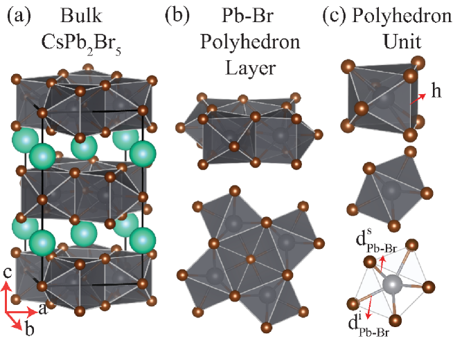
Before a detailed discussion of the potential single-layer forms of CsPb2Br5, we first investigate structural properties of bulk form of the crystal. The tetragonal phase of CsPb2Br5 is shown in Fig 1 (a). CsPb2Br5 consists of sandwiched structure with alternating Cs and Pb-Br polyhedron layers. The calculated lattice parameters are a 8.24 Å and c 14.57 Å. Tilted side and top views of Pb-Br polyhedron layer are shown in Fig 1 (b). Pb-Br polyhedron layer is composed of Pb-Br polyhedrons which are formed by putting a triangular prism and two rectangular pyramids together. Tilted side and top views of Pb-Br polyhedron are shown Fig 1 (c). There are two different bromine atoms in the polyhedron: one of them is located at the surface of Pb-Br polyhedron layer (Brs) and the other one is located at the inner plane of the layer (Bri). Bri is located in the same plane with Pb atoms and it has the Pb-Br bond distance of d 3.08 Å. The bond length between Brs and Pb atoms is d 2.92 Å. The thickness of Pb-Br polyhedron layer is h 3.83 Å. The distance between Cs and surface Br atoms is d 3.53 Å. It is found that the cohesive energy per atom of CsPb2Br5 crystal is 3.42 eV.
For detailed investigation of the bondings in CsPb2Br5 crystal Bader charge analysis is also performed. As given in the Table 1, 0.8 and 1.0 e charges are donated by each Cs and Pb atoms, respectively. On the other hand, each Br atom receives 0.6 e charge. Therefore, analysis of the electronic structure reveals that ionic interaction arises between the layers of Cs and Pb-Br skeleton via vertical charge transport from Cs layer to the Pb-Br skeleton. Furthermore, the bond between Pb and Br atoms in the Pb-Br skeleton has also an ionic character. Cs terminated surface of CsPb2Br5 crystal has a low work function of 1.17 eV.
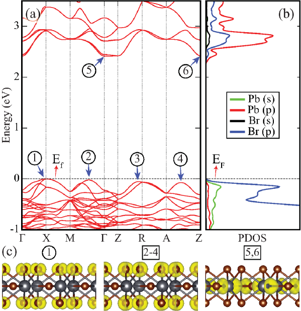
Fig. 2 shows the band structure and projected density of states (PDOS) for CsPb2Br5 crystal. It can clearly be seen from the figure, that bulk CsPb2Br5 exhibits an indirect band gap, with the valence band maximum (VBM) residing along the line -X (), while the conduction band minimum (CBM) being located at the point (). The indirect gap calculated with LDA+SOC is 2.41 eV. It is known that experimentally observed bandgaps, which are underestimated by both bare-LDA and bare-GGA functionals, can be well-approximated by the considering screening (GW calculations) and excitonic (solving Bethe-Salpeter equation) effects. However, due to high computational cost, GW and BSE calculations are not taken into account here. The partial contributions of orbital states to electronic DOS of bulk CsPb2Br5 crystal are given in the Fig. 2 (b). It appears that the major contribution to the states around the band edges originates from Pb and Br atoms. While the VBM is dominated by p orbitals of Br atom, the CBM is mostly composed of the orbitals of Pb atom. The states of the Cs atom reside at deep energy levels, therefore, they have no effect on the electronic structure of the crystal. Band-decomposed charge densities of the valence and conduction band edges are also given in the Fig. 2. As seen in the figure, edges in the top of valence band are composed of the px and orbitals of Brs atoms. Valance band edges in between and M (), Z and R (), A and Z () points differ by 23, 53 and 74 meV energy than the VBM of the single-layer, respectively. On the other hand, top of conduction band edges ( and ) are mostly made up of and orbitals of Pb atom.
IV Thinning CsPb2Br5 down to Monolayers
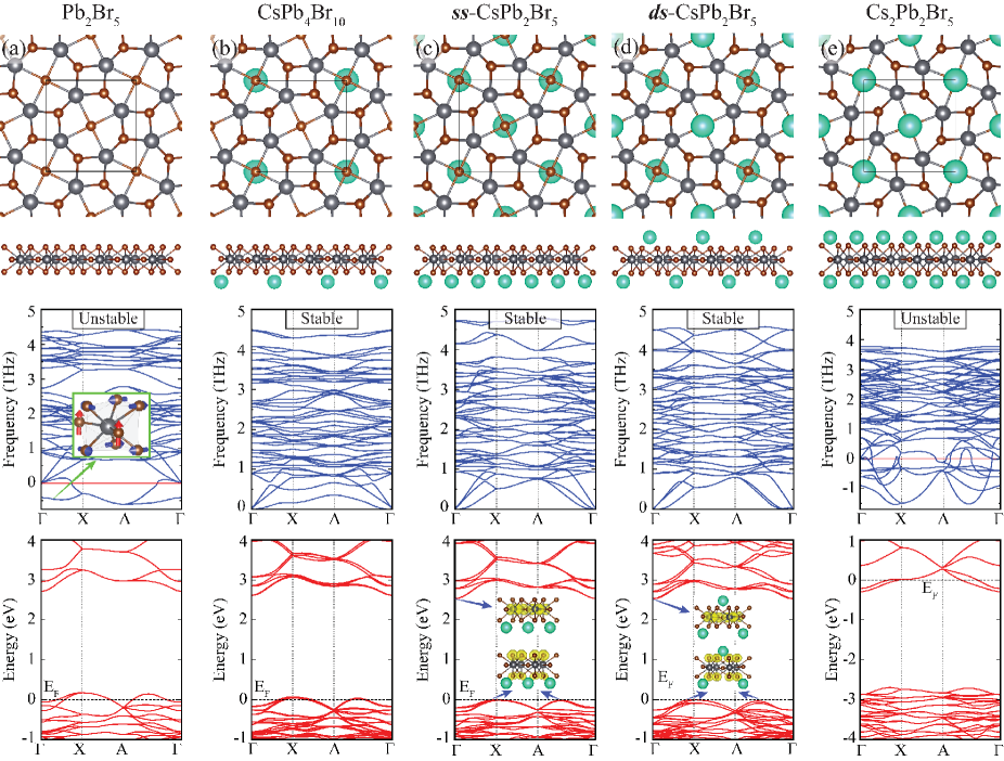
In this section, we investigate possible stable structure of single-layer CsPb2Br5 crystal and the effect of dimensional crossover on its characteristic properties. Five reasonable single-layer configurations derived from bulk CsPb2Br5 structure are shown in Fig. 3. According to their chemical compositions, these five structures are named as Pb2Br5, CsPb4Br10, single-side Cs terminated CsPb2Br5 (ss-CsPb2Br5), double-side Cs terminated CsPb2Br5 (ds-CsPb2Br5) and Cs2Pb2Br5. Depending on whether the synthesis technique is growth or mechanical exfoliation process one of these of the single layer crystal structures or their mixtures can be obtained.
Single-layer Pb2Br5 is a Cs-free skeleton composed of only Pb-Br polyhedrons. As given in Table 1, the calculated lattice parameter and thickness of Pb2Br5 are a 8.09 Å and h 3.72 Å, respectively. These values are relatively small compared to those of bulk. The calculated bond lengths between the atoms of the structure are given in the Table 1. To assess the dynamical stability, phonon dispersions of single-layer Pb2Br5 are calculated and shown in Fig. 3 (a). A 331 supercell is used for the phonon band structure calculations of single-layer forms of the crystal. The phonon spectra of the structure exhibit imaginary eigenvalues through all the symmetry points, indicating the instability of the structure. Instability in the structure could be attributed to the charge transfer mechanism between ions of the structure. As given in Table 1, resulting charges of Br atoms of Pb2Br5 are lower than that of bulk CsPb2Br5. Although each Pb atom donates 1.0 e charge, each Bri and Brs atoms receive 0.5 and 0.4 e charges, respectively. Therefore, unsaturated Bri and Brs atoms may lead to dynamical instability in single-layer Pb2Br5.
For a deeper analysis of instability of single-layer Pb2Br5, atomic displacements of the lowest mode are shown in the inset of phonon band diagram of Fig. 3 (a). It appears that the mode responsible for the instability of the structure is due to vibrations of Bri and Brs atoms normal and parallel to the plane of the structure, respectively. Imaginary eigenfrequencies in the whole Brillouin Zone indicate the lack of required restoring force against these atomic motions. Therefore, the structure is unstable under this motion and transforms to another phase. This instability can be cured by increasing the bond strength between Pb and Br atoms through adding an extra charges.
As shown in the Fig. 3 (b), single-layer of CsPb4Br10 is formed through half of the single-side of Pb-Br layer covered by Cs atoms. The lattice parameter and the thickness of the structure are a 8.18 Å and h 3.77 Å, respectively. It is found that the single-layer CsPb4Br10 is formed by a cohesive energy of 3.21 eV. Since one side of the structure is covered by Cs atoms, the bonds show anisotropy in the vertical direction (see Table 1). Given values of the bond lengths belong to Cs terminated side of the structure. The phonon spectra of single-layer CsPb4Br10 exhibit real eigenvalues through all the symmetry points, confirming the dynamical stability of the layers. Bader charge analysis shows that Cs and Pb atoms of the structure donate 0.8 and 1.0 e charges, respectively. Therefore the amount of received charges by each Br atom is 0.5 e. The work function of the structure is calculated to be 4.53 eV. It is also seen from the Fig. 3 (b) that lowering the concentration of Cs atoms leads to unfilling of the valence band edge and therefore p-type conductivity in the single-layer CsPb4Br10.
Relaxed geometric structures of ss-CsPb2Br5 and ds-CsPb2Br5 are shown in Figs. 3 (c) and (d), respectively. These two structures possess the same chemical composition with the CsPb2Br5 crystal. The lattice parameters of both of the structures are a 8.29 Å. The thickness of the Pb2Br5 sublayer of ss-CsPb2Br5 and ds-CsPb2Br5 are h 3.85 and 3.81 Å, respectively. As given in the Table 1, the atom-atom bond distances of these two structures are very similar to that of the bulk CsPb2Br5. Real frequencies in the phonon spectra of single-layer structures (Figs. 3 (c) and (d)) of ss-CsPb2Br5 and ds-CsPb2Br5 appear in a whole Brillouin Zone, indicating the dynamically stabilities of these two structures. Bader charge analysis reveals that the charge transfer mechanism of single-layers of ss-CsPb2Br5 and ds-CsPb2Br5 are very similar to the bulk CsPb2Br5. Cs and Pb atoms of the both structures donate 0.8 and 1.0 e charges, respectively. The amount of charge received by Br atoms of the two structures are in the range of 0.5-0.6 e. Therefore, Pb-Br skeletons of the two structures are saturated with enough charges to maintain stable bonding mechanism. In addition, cohesive energies of these two structures are given in Table 1. Among the single-layer forms of the crystal, due to the vertical symmetry and the same chemical composition with the bulk counterpart, ds-CsPb2Br5 has the highest cohesive energy. Furthermore, calculated work function values of singe-layers of ss-CsPb2Br5 and ds-CsPb2Br5 are 2.75 and 4.79 eV, respectively. Calculated values of the work functions belong to Cs-terminated side of the structure. Hence, the work function shows a decreasing behavior with increasing concentration of Cs atoms of Cs-terminated side. As shown in Fig. 3 (c) and (d), single-layer ss-CsPb2Br5 and ds-CsPb2Br5 have very similar electronic band diagrams and they are indirect band gap semiconductors. The VBMs of the two structures reside at X point, whereas their CBMs reside at point. It is worth mentioning that valence band edge in between A and points differs only by 24 meV energy from the VBM of the two structure. Band decomposed charge densities at the valence band and the conduction band edges of the two structures are shown in Figs. 3 (c) and (d). Band edge characteristics of these structures possess very similar behavior with their bulk counterpart. As given in Table 1, the SOC included band gap of ss-CsPb2Br5 and ds-CsPb2Br5 are 2.53 and 2.54 eV therefore with decreasing thickness from bulk to single-layer, the band gap of CsPb2Br5 increases by 0.13 eV.
The single-layer Cs2Pb2Br5 is constructed by three submonolayers: a Pb2Br5 sublayer and two surrounding sublayers of Cs atoms. The calculated lattice parameter of Cs2Pb2Br5, a 8.21 Å is very similar to bulk lattice parameter of the crystal. However, the thickness of Pb2Br5 sublayer is h 4.31 Å, which is much higher than that of the other single-layer forms of the crystal. As in Pb2Br5, phonon spectra of single-layer Cs2Pb2Br5, shown in Fig. 3 (e), exhibit imaginary eigenvalues through whole the symmetry points, indicating the dynamical instability of the structure. In single-layer Cs2Pb2Br5, while each Cs and Pb atom donate 0.8 e charges, each Bri and Brs atoms receive 0.6 and 0.7 e charges, respectively. Extra charges provided by Cs atoms lead to a decrease in charge transfer between Pb and Br atoms. Therefore, the Cs-induced weakening of the Pb-Br bonds is the reason of the instability in the single-layer Cs2Pb2Br5.
IV.1 Effect of Cs Atoms via The Charging of Pb2Br5 Skeleton
In this chapter, in order to facilitate a deeper understanding of the role of Cs atoms, we examine the stability of Cs-free Pb2Br5, which is already presented to be unstable in the previous chapter, via charging calculations.
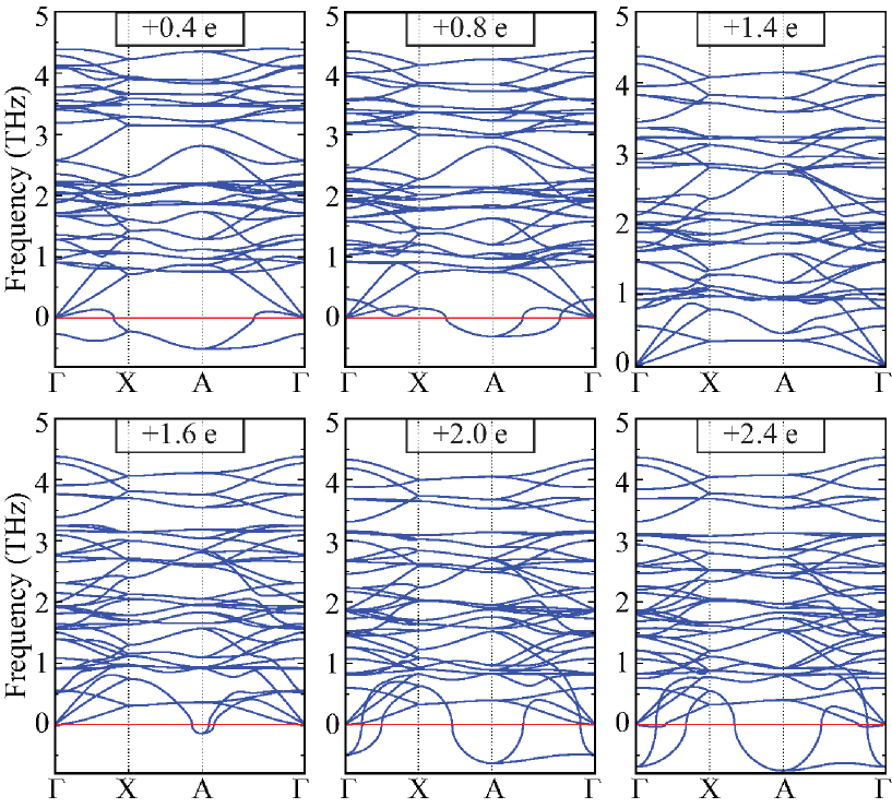
One low-lying optical and one acoustic phonon branches that have imaginary eigenfrequencies are the direct indication of dynamical instability in the single layer structure of Cs-free Pb2Br5. However, as calculated in the previous chapter, single layer skeleton structure of Pb2Br5 can be stabilized through the adsorption of Cs atoms. Therefore, the question arises as to whether or not the stability of CsPb2Br5 is provided only by the charge transferred from Cs atoms to Pb2Br5 skeleton.
As shown in Fig. 4, the role of electron transfer on the stability of Pb2Br5 can be examined through the addition of extra electrons into the primitive unit cell. Here, it is important to note that once the unit cell is charged by extra electrons, structure is re-optimized by considering the new charge distribution and phonon calculations are performed for this fully-relaxed structure. Fig. 4 shows that one acoustic and one low-lying optical branches, having imaginary eigenfrequencies, of the Pb2Br5 skeleton can be fixed upon the charging. It appears that while the structure is fully stabilized under 1.4 e charging, it exhibits instability under over-charged and less-charged situations. Therefore, it can be concluded that Cs atoms play an important role as stabilizer of the Pb2Br5 skeleton by charge transfer. Such a charge dependent stability may pave the way to synthesize novel Cs-free perovskite structures and to fix the vacancy-dependent instabilities in similar structures.
V Vacancy Defects in Single-Layer CsPb2Br5
During the growth or exfoliation of layered crystals, existence of various lattice imperfections is inevitable. One of the most common lattice imperfection in layered crystals is vacancies. The formation of vacancies in ionically bonded materials are the source of trap states and profoundly alter the electronic and optical properties of semiconductors. Therefore, it is important to investigate how vacancies are formed and what are the characteristic features. In this section, four different vacancy types in single-layer ds-CsPb2Br5 that corresponds to the energetically the most favorable structure are considered, Cs vacancy (VCs), Bri vacancy (V), Brs vacancy (V), and Pb vacancy (VPb). In order to hinder the interaction between vacancies in adjacent cells, a 64-atom supercell was used. Relative stabilities of the four vacancies are calculated according to the formula:
| (2) |
where Eform is the formation energy of the relevant vacancy, ESL+vac is the total energy of the supercell with vacancy, EA is the isolated-single-atom energy of the removed atom and ESL is the total energy of supercell of single layer.
| a | Eform | M | Electronic | Band Gap | |
|---|---|---|---|---|---|
| (Å) | (eV) | () | Characteristic | (eV) | |
| VCs | 16.48 | 4.82 | 0.0 | semiconductor | 2.53 |
| V | 16.44 | 5.02 | 1.0 | semiconductor | 0.12 |
| V | 16.48 | 4.51 | 1.0 | semiconductor | 0.25 |
| VPb | 16.46 | 8.20 | 0.0 | metal | - |
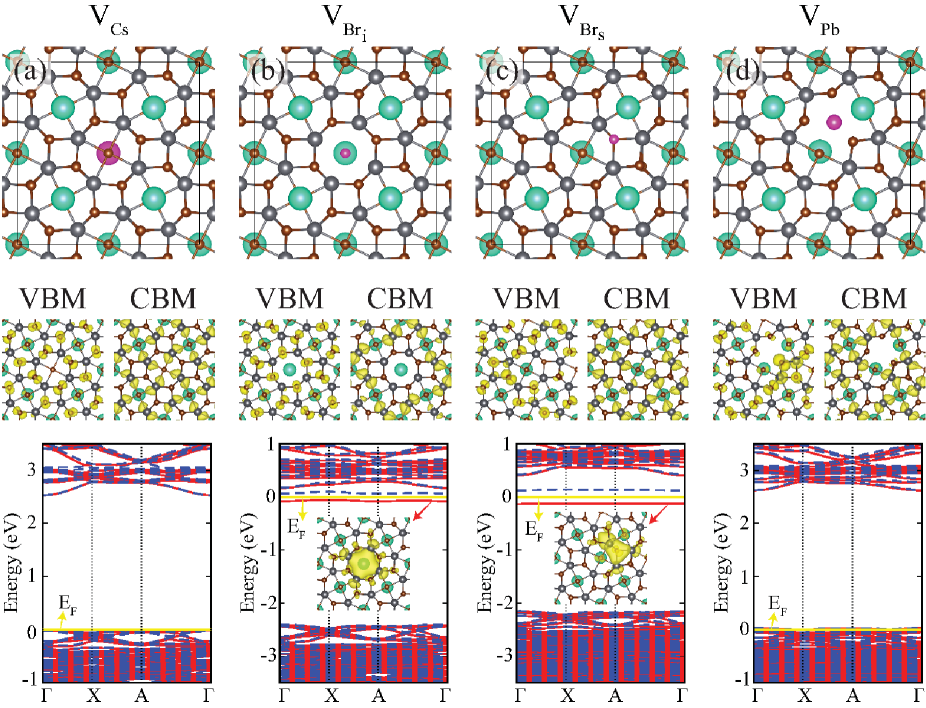
Relaxed geometric structures when a single Cs, Bri, Brs and Pb are created in the ds-CsPb2Br5 are shown in Figs. 5 (a)-(d), respectively. Formation of these vacancies leads to negligible distortion on the single-layer ds-CsPb2Br5. As given in the Table 1 fully relaxed lattice parameters of VCs, V, V and VPb are 16.48, 16.44, 16.48 and 16.46 Å, respectively. The formation of Pb vacancy (VPb) leads to minor local reconstructions. When Pb vacancy is introduced, the closest Br atoms to the extracted Pb atom are released and they move toward the neighboring Pb atoms. The formation energies of VCs, V, V and VPb are calculated to be 4.82, 5.02, 4.51 and 8.20 eV, respectively. Therefore, one can conclude that formation of Cs and Br vacancies in single-layer ds-CsPb2Br5 perovskite are more likely.
The electronic band structures of ds-CsPb2Br5 with VCs, V, V and VPb are presented in Figs. 5 (a)-(d), respectively. It appears that electronic properties of single-layer ds-CsPb2Br5 do not change significantly with the removal of Cs atom. Band decomposed charge densities at the valence band and conduction band edges of VCs show similar behavior with that of pristine ds-CsPb2Br5. Figs. 5 (b) and (c) display band decomposed charge densities and electronic band diagrams of V and V. It is seen that only the formation of Br vacancies leads to presence of in-gap states. Such dispersionless electronic states can be attributed to the unpaired electrons of neighboring Pb and Br atoms. For V and V vacancies, two spin-polarized in-gap states are symmetrically placed around the Fermi level with band gaps of 0.12 and 0.25 eV, respectively, which then describe a singly occupied in-gap state with a magnetic moment of 1 . Fig. 5 (d) shows that when formation of Pb vacancy is created, some states of ds-CsPb2Br5 discharge due to the lack of donor electrons of Pb atom. As a result, formation of Pb vacancy leads to p-type conductivity in single-layer ds-CsPb2Br5.
VI Conclusions
In conclusion, using first-principle calculations, we investigated the structural, electronic and vibrational properties of CsPb2Br5 crystal, and how these properties are affected by dimensional crossover. Bulk CsPb2Br5 is an indirect bandgap semiconductor with a bandgap of 2.41 (LDA+SOC) eV. It was calculated that while the valence and conduction band edges of bulk CsPb2Br5 crystal are mainly composed of Pb and Br atoms, Cs atoms do not play role in electronic properties.
Then, we predicted that there are two dynamically stable phases of single layer CsPb2Br5. These two structures were found to be stable in both total energy optimization and phonon calculations. Single-layer structures of CsPb2Br5 display indirect semiconducting character with a band gap of 2.54 eV within LDA+SOC. Moreover, we showed that stability of single layer CsPb2Br5 structures strongly depend on the concentration of Cs atoms. As supported by charging-dependent phonon dispersion calculations, Cs atoms provide stability by 0.8 per atom charge transfer from Cs atoms to the Pb2Br5 skeleton.
In addition, formation characteristics, electronic structure, and magnetic ground state of four different vacancy types in single-layer CsPb2Br5 were investigated. It was seen that the formation of Br vacancy is the most likely one and it leads to emergence of localized in-gap states. Moreover, single-layer ds-CsPb2Br5 has a ferromagnetic ground state upon the formation of Br vacancies. On the other hand, p-type doping occurs in semiconducting single-layer CsPb2Br5 when Pb and Cs vacancies are formed.
VII acknowledgments
Computational resources were provided by TUBITAK ULAKBIM, High Performance and Grid Computing Center (TR-Grid e-Infrastructure). HS acknowledges financial support from the TUBITAK under the project number 116C073. HS acknowledges support from Bilim Akademisi-The Science Academy, Turkey under the BAGEP program.
References
- (1) M. Grätzel, Nat. Mater. 13, 838 (2014).
- (2) Z. -K. Tan, R. S. Moghaddam, M. L. Lai, P. Docampo, R. Higler, F. Deschler, M. Price, A. Sadhanala, L. M. Pazos, D. Credgington, F. Hanusch, T. Bein, H. J. Snaith, and R. H. Friend, Nat. Nanotechnol. 9, 687 (2014).
- (3) L. Dou, Y. M. Yang, J. You, Z. Hong, W. -H. Chang, G. Li, and Y. Yang, Nat. Commun. 5, 5404 (2014).
- (4) H. Zhu, Y. Fu, F. Meng, X. Wu, Z. Gong, Q. Ding, M. V. Gustafsson, M. T. Trinh, S. Jin, and X. -Y. Zhu, Nat. Mater. 14, 636 (2015).
- (5) W. S. Yang, J. H. Noh, N. J. Jeon, Y. C. Kim, S. Ryu, J. Seo, and S. I. Seok, Science 348, 1234 (2015).
- (6) Y. -H. Kim, H. Cho, J. H. Heo, T. -S. Kim, N. Myoung, C. -L. Lee, S. H. Im, and T. -W. Lee, Adv. Mater. 27, 1248 (2015).
- (7) J. Xing, F. Yan, Y. Zhao, S. Chen, H. Yu, Q. Zhang, R. Zeng, H. V. Demir, X. Sun, A. Huan, and Q. Xiong, ACS Nano 10, 6623 (2016).
- (8) J. H. Noh, S. H. Im, J. H. Heo, T. N. Mandal, and S. I. Seok, Nano Lett. 13, 1764 (2013).
- (9) O. Ergen, S. M. Gilbert, T. Pham, S. J. Turner, M. T. Z. Tan, M. A. Worsley, and A. Zettl, Nat. Mater. 16, 522 (2017).
- (10) N. J. Jeon, J. H. Noh, W. S. Yang, Y. C. Kim, S. Ryu, J. Seo, and S. I. Seok, Nature 517, 476 (2015).
- (11) L. Protesescu, S. Yakunin, M. I. Bodnarchuk, F. Krieg, R. Caputa, C. H. Hendon, R. X. Yang, A. Wanlsh, and M. V. Kovalenko, Nano Lett. 15, 3692 (2015).
- (12) M. Kulbak, D. Cahen, and G. Hodes, J. Phys. Chem. Lett. 6, 2452 (2015).
- (13) Y. Wang, X. Li, J. Song, S. Xiao, H. Zeng, and H Sun, Adv. Mater. 27, 7101 (2015).
- (14) A. Swarnkar, R. Chulliyil, V. K. Ravi, D. M. Irfanullah, D. A. Chowdhury, and D. A. Nag, Angew. Chem. 127, 15644 (2015).
- (15) X. Li, Y. Wu, S. Zhang, B. Cai, Y. Gu, J. Song, and H. Zeng, Adv. Func. Mater. 26, 2435 (2016).
- (16) G. R. Yettapu, D. Talukdar, S. Sarkar, A. Swarnkar, A. Nag, P. Ghosh, and P. Mandal, Nano Lett. 16, 4838 (2016).
- (17) J. Kang and L. -W. Wang, J. Phys. Chem. Lett. 8, 489 (2017).
- (18) K. S. Novoselov, A. K. Geim, S. V. Morozov, D. Jiang, Y. Zhang, S. V. Dubonos, I. V. Grigorieva, and A. A. Firsov, Science 306, 666 (2004).
- (19) K. F. Mak, C. Lee, J. Hone, J. Shan, and T. F. Heinz, Phys. Rev. Lett. 105, 136805 (2010).
- (20) A. Splendiani, L. Sun, Y. Zhang, T. Li, J. Kim, C. -Y. Chim, G. Galli, and F. Wang, Nano Lett. 10, 1271 (2010).
- (21) J. A. Sichert, Y. Tong, N. Mutz, M. Vollmer, S. Ficher, K. Z. Milowska, R. G. Cortadella, B. Nickel, C. Cardenas-Daw, J. K. Stolarczyk, A. S. Urban, and J. Feldmann, Nano Lett. 15, 6521 (2015).
- (22) L. Dou, A. B. Wong, Y. Yu, M. Lai, N. Kornienko, S. W. Eaton, A. Fu, C. G. Bischak, J. Ma, T. Ding, N. S. Ginsberg, L. -W. Wang, A. P. Alivisatos, and P. Yang, Science 349, 1518 (2015).
- (23) J. Liu, Y. Xue, Z. Wang, Z. -Q. Xu, C. Zheng, B. Weber, J. Song, Y. Wang, Y. Lu, Y. Zhang, and Q. Bao, ACS Nano 10, 3536 (2016).
- (24) J. Song, J. Li, X. Li, L. Xu, Y. Dong, and H. Zheng, Adv. Mater. 27, 7162 (2015).
- (25) G. Li, H. Wang, Z. Zhu, Y. Chang, T. Zhang, Z. Song, and Y. Jiang, Chem. Commun. 52, 11296 (2016).
- (26) K. -H. Wang, L. Wu, L. Li, H. -B. Yao, H. -S. Qian, and S. -H. Yu, Angew. Chem. Int. Ed. 55, 8328 (2016).
- (27) X. Zhang, B. Xu, J. Zhang, Y. Gao, Y. Zheng, K. Wang, and X. W. Sun, Adv. Func. Mater. 26, 4595 (2016).
- (28) C. E. Giusca, I. Rungger, V. Panchal, C. Melios, Z. Lin, Y. -C. Lin, E. Kahn, A. L. Elias, J. A. Robinson, M. Terrones, and O. Kazakova, ACS Nano 10, 7840 (2016).
- (29) P. Vogt, P. D. Padova, C. Quaresima, J. Avila, E. Frantzeskakis, M. C. Asensio, A. Resta, B. Ealet, G. L. Lay, Phys. Rev. Lett. 108, 155501 (2012).
- (30) A. Fleurence, R. Friedlein, T. Ozaki, H. Kawai, Y. Wang, Y. Yamada-Takamura, Phys. Rev. Lett. 108, 245501 (2012).
- (31) Q. Wang, M. Lyu, M. Zhang, J. -H. Yun, H. Chen, and L. Wang, J. Phys. Chem. Lett. 6, 4379 (2015).
- (32) X. Zhang, X. Ren, B. Liu, R. Munir, X. Zhu, D. Yang, J. Li, Y. Liu, D. -M. Smilgies, R. Li, Z. Yang, T. Niu, X. Wang, A. Amassian, K. Zhao, and S. F. Liu, Energy Environ. Sci. (2017).
- (33) M. Saliba, T. Matsui, J. -Y. Seo, K. Domanski, J. -O. Correa-Baena, M. K. Nazeeruddin, S. M. Zakeeruddin, W. Tress, A. Abate, A. Hagfeldt, and M. Grätzel, Energy Environ. Sci. 9, 1989 (2016).
- (34) G. Kresse and D. Joubert, Phys. Rev. B 59, 1758 (1999).
- (35) P. E. Blöchl, Phys. Rev. B 50, 17953 (1994).
- (36) G. Kresse and J. Hafner, Phys. Rev. B 47, 558 (1993).
- (37) G. Kresse and J. Furthmuller, Phys. Rev. B 54, 11169 (1996).
- (38) J. P. Perdew and A. Zunger, Phys. Rev. B 23, 5048 (1981).
- (39) D. M. Ceperley and B. J. Alder, Phys. Rev. Lett. 45, 566 (1980).
- (40) G. Henkelman, A. Arnaldsson, and H. Jonsson, Comput. Mater. Sci. 36, 354 (2006).
- (41) G. Makov and M. C. Payne, Phys. Rev. B 51, 4014 (1995).
- (42) D. Alfè, Comput. Phys. Commun. 180, 2622 (2009).