Theory of the carbon vacancy in -SiC: crystal field and pseudo Jahn-Teller effects
Abstract
The carbon vacancy in -SiC is a powerful minority carrier recombination center in as-grown material and a major cause of degradation of SiC-based devices. Despite the extensiveness and maturity of the literature regarding the characterization and modeling of the defect, many fundamental questions persist. Among them we have the shaky connection of the EPR data to the electrical measurements lacking sub-lattice site resolution, the physical origin of the pseudo-Jahn-Teller effect, the reasoning for the observed sub-lattice dependence of the paramagnetic states, and the severe temperature-dependence of some hyperfine signals which cannot be accounted for by a thermally-activated dynamic averaging between equivalent Jahn-Teller distorted structures. In this work we address these problems by means of semi-local and hybrid density functional calculations. We start by inventorying a total of four different vacancy structures from the analysis of relative energies. Diamagnetic states have well defined low-energy structures, whereas paramagnetic states display metastability. The reasoning for the rich structural variety is traced back to the filling of electronic states which are shaped by a crystal-field-dependent (and therefore site-dependent) pseudo-Jahn-Teller effect. From calculated minimum energy paths for defect rotation and transformation mechanisms, combined with the calculated formation energies and electrical levels, we arrived at a configuration-coordinate diagram of the defect. The diagram provides us with a detailed first-principles picture of the defect when subject to thermal excitations. The calculated acceptor and donor transitions agree well with the binding energies of electrons emitted from the Z1/2 and EH6/7 traps, respectively. From the comparison of calculated and measured -values, and correlating the site-dependent formation energies with the relative intensity of the DLTS peaks in as-grown material, we assign Z1 (EH6) and Z2 (EH7) signals to acceptor (donor) transitions of carbon vacancies located on the and sub-lattice sites, respectively
pacs:
71.55.-i, 71.55.Cn, 71.70.Ch, 71.70.EjI Introduction
A wide and indirect band-gap, high chemical and thermal stability, as well as radiation and electrical hardness, are among the merits that make silicon carbide (SiC) an outstanding material for high-voltage and high-power electronics.Park (1998); Kimoto and Cooper (2014) Due to its superior properties, the -SiC polytype has been the material of choice of the industry. However, the presence of carbon-related point defects in SiC, particularly carbon vacancies (VC), is a major cause for minority carrier recombination in n-type material and device failures like low field effect mobility.Iwamoto and Svensson (2015); Nipoti et al. (2015) These problems have been connected to a set of VC-related deep traps measured by deep-level transient spectroscopy (DLTS) and labelled Z1/2 and EH6/7.Kimoto et al. (1995); Hemmingsson et al. (1997); Hiyoshi and Kimoto (2009)
The Z1/2 has been ascribed to the superposition of Z1 and Z2 signals, each of which arising from a two-electron emission cascade at distinct sub-lattice sites of the polytype.Hemmingsson et al. (1998, 1999); Son et al. (2012) Defects behaving like that are said to possess a negative- as they show an inverted order of energy levels.Watkins (1984) This is possible thanks to a strong atomic relaxation somewhere along the emission sequence. For the case of Z1/2 this translates into the appearance of a occupancy level at about eV, implying that the formation of negatively charged vacancies () is always energetically unfavorable against the formation of any mix of neutral () and double negative () defects, no matter the position of the Fermi energy. The appearance of is most likely when the Fermi level lies at the transition energy, where its formation energy, , is lowest with respect to other charge states. Depending on the temperature and the energy difference , some states can still be populated. Alternatively, can be formed from other charge states after capture/emission of carriers upon optical excitation. The actual and levels were respectively measured at 0.67 eV and eV below , whereas and were found at about eV and eV, respectively.Hemmingsson et al. (1998, 1999); Son et al. (2012) Also noteworthy is the fact that in -SiC, a pair of electron traps located at eV and labelled E1/E2 from DLTS measurements, were attributed to acceptor transitions from equivalent defects at different sub-lattice sites.Dmowski (1990); Aboelfotoh and Doyle (1999) More recently, high-resolution Laplace-DLTS was able to further resolve E1/E2 into three components, and based on their similarity with Z1/2 (including their capture cross section and negative- ordering of levels), they were assigned to the carbon vacancy located on all three available sites (, and ) of the polytype.Koizumi et al. (2013)
The EH6/7 DLTS band has been a subject of discussion and surrounded by some controversy. It usually shows up with a magnitude lower than Z1/2,Ayedh et al. (2014) and it is made of two nearly overlapping peaks, apparently with varying amplitude ratio (between 1:3 and 1:5) depending on sample conditions.Danno and Kimoto (2006); Booker et al. (2016) These facts led to suggestions that EH6/7 should not have the same origin of Z1/2, but rather be connected to a complex involving VC.Storasta et al. (2004); Reshanov et al. (2007); Zippelius et al. (2011); Alfieri and Kimoto (2013) Recently, Booker and co-workersBooker et al. (2016) analyzed the EH6/7 capacitance transients, and based on a three-charge state model they concluded that like Z1/2, the EH6/7 band results from two correlated, two-electron emission processes from two defects. Most importantly, they found that the concentration ratio of EH6:EH7 is 1:1 if we consider that the stronger peak actually combines EH, EH and EH transitions, while the smaller component of the band comes from EH alone. The issue of the inconsistent magnitude ratio between EH6/7 and Z1/2 was poorly addressed. For all these transitions, carrier binding energies were measured at eV, eV, eV and about eV, respectively. This suggests that EH7 is a negative- defect, while that cannot be said for EH6 due to uncertainty in the measurements.
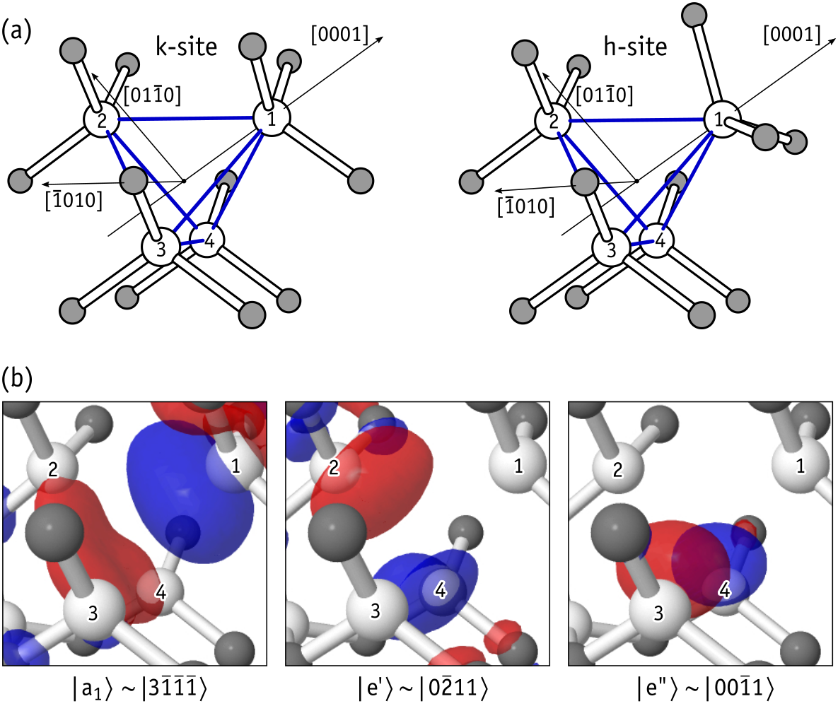
Before continuing, let us introduce some notation with the help of Figure 1(a). Here we depict the atomic structure of perfect VC defects at - and -sites (with and labels referring to quasi-cubic and quasi-hexagonal sub-lattice sites of the -SiC crystal). For the sake of convenience, the atom numbering scheme was chosen in line with previous works in the literature.Bockstedte et al. (2003); Umeda et al. (2004a) Hence, for a trigonal structure we have Si1 (axial) and Si (basal) shells of Si atoms. For monoclinic structures we assume Si1 and Si2 to lie on the mirror plane and the Si3,4 pair to be mirror-symmetric. Hereafter, V refers to the carbon vacancy at the sub-lattice site and charge state (from double minus to double plus). Occasionally we may also distinguish a vacancy with a specific atomic geometry as V. We also introduce at this point a way to represent the vacancy electronic states using simple linear combination of atomic orbitals (LCAO). Accordingly, a state stands for , where is a normalization constant, are hybridization coefficients, and the summation runs over all four Sii radical states (with ).
Many details about the electronic and atomistic structure of VC in -SiC, particularly in their paramagnetic and states, could be unraveled by electron paramagnetic resonance (EPR) measurements.Son et al. (2001); Zvanut and Konovalov (2002); Konovalov et al. (2003); Umeda et al. (2004b); Bratus’ et al. (2005); Umeda et al. (2005); Son et al. (2012); Trinh et al. (2013) Among these reports, those combining experiments with first-principles calculationsUmeda et al. (2004a); Bratus’ et al. (2005); Umeda et al. (2005); Trinh et al. (2013) turn out to be particularly elucidating. Below we provide a brief summary of those results, with a special focus on the relevant issues for the purpose of this work.
In p-type material irradiated with MeV electrons at high temperatures (850∘C), the EPR spectrum revealed two signals, labelled as EI5 (also referred to as Ky1/Ky2/ID1) and EI6 (also Ky3/ID2), which were assigned to and , respectively.Zvanut and Konovalov (2002); Konovalov et al. (2003); Umeda et al. (2004b, a); Bratus’ et al. (2005) Below K the main line of exhibited symmetry, and was accompanied by three distinct hyper-fine (HF) signals due to interactions between the electron spin and 29Si nuclei in shells with 1, 1 and 2 atoms. Above 50 K the spectrum was converted to a trigonal () pattern with two HFs representative of 1 axial Si atom and 3 equivalent Si atoms on the basal plane. From the temperature dependence of the HF life-times, the conversion from monoclinic to trigonal symmetry was estimated to be limited by a barrier as low as 0.014 eV.Umeda et al. (2004a) on the other hand, always showed trigonal symmetry irrespectively of the temperature of the measurement (down to K). The HF structure consisted of two line pairs with about 1:3 intensity ratio when the magnetic field was aligned along [0001]. However, unlike for V at the cubic site, the HF principal direction of the basal radicals of V strongly deviated from the perfect tetrahedral angle, and shifted from 103 down to 98° as the temperature was lowered from 150 K to 10 K. This behavior was interpreted as an increase of the anti-bonding character between the axial and basal radicals when the temperature was lowered.Umeda et al. (2004b)
Most observations described above were accounted for by density-functional calculations. They arrived at ground state structures and HF tensors compatible with the low-temperature EPR data.Bockstedte et al. (2003); Umeda et al. (2004a); Bratus’ et al. (2005) According to the calculations, V and V defects adopt and geometries in the ground state, with their highest (semi-)occupied Kohn-Sham states (HOKS) possessing and symmetry, respectively. Within the above LCAO picture they can be approximately described as and , respectively, explaining the HF structure observed for V and V at low-temperatures ( K). They are also consistent with the measurements of V at K if we assume that above this temperature the defect assumes a motional-averaged trigonal state due to fast hopping between all three , and degenerate structures neighboring the undistorted () configuration. Note that in line with the observations, all Si radicals contribute to in V (under static and dynamic conditions), and the amplitude of the axial radical in the state accounts for about 50% of the total LCAO localization in V. The paramagnetic state of V is also consistent with the observed anti-bonding character between Si1 and the basal Si radicals. However, the model is still unable to account for the magnitude of the high-temperature ( K) HF signals. Another puzzle, which was noted by Bockstedte and co-workers,Bockstedte et al. (2003) is that despite being a singlet state, the trigonal V configuration is unstable against monoclinic distortion, implying the influence of a pseudo-Jahn-Teller (pJT) effect. However, neither was a justification provided for its manifestation, nor was it found why a similar effect is apparently missing in V.
Negatively charged carbon vacancies were observed by EPR in n-type -SiC irradiated either with MeV electrons at 850∘C or with 250 keV electrons at room temperature.Umeda et al. (2005); Son et al. (2012) Although some traces of V and V signals could be detected above K in darkness (in heavily doped material),Son et al. (2012) most experiments were performed on illuminated samples, which gave rise to much stronger signals.Umeda et al. (2005); Son et al. (2012); Trinh et al. (2013) At the cubic site and below K, the V main line showed a monoclinic pattern and a single HF pair related to two symmetry-equivalent Si nuclei (Si3,4).Trinh et al. (2013) Additional and weaker HF signals were related to more distant shells. Above K the Si3,4 HF signal disappeared from the spectrum and the main line acquired a trigonal pattern, accompanied by the appearance of a new axial HF pair (due to interaction between a magnetic Si1 nucleus and the electron spin). As the temperature further increased, the magnitude of the Si1 HF splitting increased and at 80-90 K a weak and broad HF pair accounting for three equivalent (Si) nuclei appeared in the spectrum as well.Trinh et al. (2013) Regarding V, the main signal is monoclinic at K and below. At these temperatures two HF signal pairs related to two inequivalent Si nuclei (Si1 and Si2) with site symmetry were detected. Raising the temperature above K led to the broadening and disappearance of the Si2 HF, while the main-line and Si1 HF components merged into single trigonal peaks. The activation barrier for the monoclinic-trigonal conversion was estimated as 0.02 eV.Umeda et al. (2005) Within the temperature range of 70-120 K only the Si1 HF was detected, but when K a trigonal HF signal representative of three equivalent Si nuclei (Si) was also observed.
Again, first-principles modeling played a key role in grasping several of the above features.Zywietz et al. (1999); Umeda et al. (2005); Trinh et al. (2013) Recent density functional calculations indicated that V has a paramagnetic ground state, whereas the symmetric state was metastable by only 0.03 eV.Trinh et al. (2013) The calculated HF tensors for Si3,4 radicals accounted very well for the low-temperature ( K) experimental data. The quenching of the Si3,4 HF signal above 40 K and the observation of trigonal hyperfine structures at higher temperatures was suggested to result from the partial population of both and states. Accordingly, under these conditions they would quickly hop between three equivalent Jahn-Teller (JT) distorted alignments. While this picture aims at accounting for the observed non-zero amplitude of the wave-function on all four radicals above 90 K, it cannot be correct. Any sequential transformation between and states involves an intermittent quenching of the spin-density on the basal nuclei. Further, the model could not explain why there is a K gap between the quenching of the Si3,4 HF signal (at 40 K) and the appearance of the Si HF signal (at 80 K). Also puzzling and unexplored was the fact that the V ground state was found to be nodal (), which in principle has higher kinetic energy than the metastable state (). Finally, the symmetry lowering of V cannot simply be explained by the JT effect. In the perfect vacancy ( symmetry), the four Si radicals hybridize into a fully occupied valence state , and three gap states , and to be populated with three electrons. We calculated these states for an undistorted (trigonal) vacancy at the -site using the same method of Ref. Trinh et al., 2013 and they are depicted in Figure 1(b). The latter two are higher in energy and represent orthogonal components of a doublet which is split from due to the internal crystal field. For the case of V the doublet becomes partially populated (with a single electron) and the JT effect is expected to split (within ) into (within ), where the upward arrow stands for the paramagnetic electron. Now, while the first-principles results from Ref. Trinh et al., 2013 indicate that the metastable state has amplitude on Si1, it is clear from Figure 1(b) that a JT-split component cannot account for this feature.
Turning now to V, the calculations arrived at a ground state rather different than that found for the cubic site, namely the unpaired electron was localized on the Si1-Si2 pair as .Zywietz et al. (1999); Umeda et al. (2005) The calculated HF tensor elements for both (inequivalent) Si1 and Si2 radicals agreed very well with the measurements below K (both in magnitude and principal directions), providing compelling evidence for the correctness of the model. The disappearance of the Si2 HF signal together with the conversion of the -symmetric Si1 HF into a trigonal signal at K was justified based on a thermal activated hopping between , and equivalent states, which preserves a steady wave function amplitude only on Si1.Umeda et al. (2005) Again, the reasoning for a 70-120 K temperature window where only Si1 HF was observed and above which another trigonal Si HF was observed, was left unaddressed. Analogously to the metastable structure in the cubic site, the electronic structure of V in the ground state involves a non-vanishing spin-density on Si1. Hence, unlike suggested in Ref. Umeda et al., 2005, the model cannot be explained by the JT effect, simply because none of the -components in Fig. 1(b) shows non-zero amplitude on Si1. Finally, V and V show monoclinic ground-states with opposite symmetry with respect to the mirror plane. Although the calculations were successful in accounting for the observed site-dependent ordering of electronic states,Zywietz et al. (1999); Umeda et al. (2005) again the reasonings behind this effect were left unaddressed.
The connection of (via EPR) with the Z1/2 and EH6/7 traps (via DLTS) was suggested based on the correlation between the position of the DLTS levels and the photo-EPR excitation thresholds for and , respectively (where represent a free electron at the conduction band bottom).Son et al. (2012) More recently, Kawahara et al.Kawahara et al. (2013, 2014) investigated samples irradiated by low-energy (250 keV) electrons, which could displace C atoms only. In those works they reported a good correlation between the area density of EPR active and the fraction of carriers trapped by the dominant Z1/2 on samples irradiated with different electron fluences.
It seems clear that Z1/2 is a negative- center. This is consistent with the need of optical excitation in order to observe negatively charged vacancies by EPR. However, that is not the case for the defect responsible for EH6/7. In recent state-of-the-art electrical level calculations using many-body perturbationBockstedte et al. (2010) and hybrid density functionalHornos et al. (2011) methods, the donor levels were predicted to be separated by a small positive or essentially zero -value ( eV). While this agrees with the low-temperature EPR measurements in darkness, it is also in apparent conflict with the negative- ordering reported for EH7 and tentatively proposed for EH6 from DLTS.Booker et al. (2016) As a word of caution, we note that when periodic charge corrections were neglected, the calculations clearly indicated for both acceptors and donors.Zywietz et al. (1999); Bockstedte et al. (2010); Trinh et al. (2013)
It is clear that despite many advances, there are several fundamental puzzles to be solved. This paper aims at addressing those issues, as well as others that will become evident further ahead. In this section we wanted to introduce the reader to the main properties of the carbon vacancy in -SiC, how the EPR data has been related to the prominent Z1/2 and EH6/7 electron traps, and the importance of theory/computational modeling in providing models and checking their quality. We will now proceed with a description of the theoretical methods followed by the main results. These include the reproduction of structures and electronic levels previously reported, as well as new results like a physical description ofthe observed pseudo-Jahn-Teller distortions, the crystal-field impact on the distinct electronic structure of cubic and hexagonal vacancies, and the atomistic mechanisms behind the -dependent dynamic effects observed by EPR. Before the conclusions, we also include a section where we discuss the above issues.
II Theory
The calculations were carried out using the VASP package,Kresse and Hafner (1993, 1994); Kresse and Furthmüller (1996a, b) employing the projector-augmented wave (PAW) method to avoid explicit treatment of core electrons.Blöchl (1994) A plane wave basis set with kinetic energy up to 400 eV was used to describe the electronic Kohn-Sham states. The many-body electronic potential was evaluated using the hybrid density functional of Heyd-Scuseria-Ernzerhof (HSE06),Heyd et al. (2003); Krukau et al. (2006) which mixes semi-local and exact exchange interactions at short ranges, treating the long-range interactions within the simpler generalized gradient approximation as proposed by Perdew, Burke and Ernzerhof (PBE).Perdew et al. (1996) When compared to plain PBE calculations, HSE06 has the main advantage of predicting a Kohn-Sham (indirect) band gap 3.17 eV wide for -SiC, which should be compared to the experimental value of 3.27 eV.Grivickas et al. (2007) To a large extent, this approach mitigates the well known underestimated gap syndrome affecting PBE-level calculations, which show a 2.19 eV band gap width. Although most results reported below were obtained using the HSE06 method, PBE-level results are also included and in that case they are explicitly identified.
We used 576-atom hexagonal supercells, obtained by replication of unit cells, from where a carbon atom was removed to produce a VC defect. The equilibrium (calculated) lattice parameters of -SiC were Å and 2 Å. These are close to the experimental values of Å and Å extrapolated to K.Li and Bradt (1986) All defect structures were optimized within PBE-level, using a conjugate-gradient method until the forces acting on the atoms were lower than 10 meV/Å. After this step, we took the relaxed structure, and self-consistent energies, electron and spin densities were finally obtained within HSE06. Electronic relaxations were computed with a numerical accuracy of 1 , and the band structures were solved at in reciprocal lattice units. This is conventionally referred to as the -point in the hexagonal Brillouin zone (BZ). We found this particular -point to provide the best compromise between sampling accuracy and computational performance. It is representative of the -point set in non-relativistic calculations, it led to energy differences with an error bar of about 5 meV (when compared to results obtained using sampled BZ), and most importantly, it did not cause so strong hybridization between defect levels lying high in the gap and the conduction band states as in the -sampled PBE calculations of Ref. Trinh et al., 2013.
The above two-step recipe to obtain hybrid density-functional energies using structures that were previously relaxed within PBE (hereafter referred to as pseudo-relaxed energies), casts doubts regarding its accuracy when compared to fully-relaxed HSE06-energies obtained by minimizing HSE06-forces. To clarify this issue, we compared energies and forces of pseudo- and fully-relaxed V and V states. These two charge states have rather different structures (to be discussed below), and while V does not have electrons occupying gap levels, V has two fully occupied gap states, one of them being close to the conduction band edge. These tests were carried out using 256-atom supercells ( unit cells) with a -centered grid of -points for BZ sampling. Accordingly, we obtained fully-relaxed HSE06-energies 13 meV and 11 meV below the energy of pseudo-relaxed V and V calculations, respectively. Despite these small relaxation energies, the average HSE06-force acting on Si-atoms on PBE-relaxed structures were 0.28 eV/Å and 0.10 eV/Å for for V and V, respectively, and therefore cannot be neglected. However, the energy difference was 39.384 eV and 39.386 eV for pseudo-relaxed and fully-relaxed calculations, respectively, suggesting that the error of pseudo-relaxed energy differences is of the order of a few meV.
The energy of a charged defect, when calculated using periodic boundary conditions, is actually the energy of a supercell contaminated by artificial Coulomb interactions across an array of charged defects embedded on a compensating background charge.Makov and Payne (1995) These interactions are long-ranged and difficult to remove. Several post-processing recipes have been proposed to mitigate this problem (see for example Ref. Komsa et al., 2012 and references therein). Here we use the method by Freysoldt, Neugebauer and Van de Walle,Freysoldt et al. (2009) recently generalized for anisotropic materials.Kumagai and Oba (2014) Accordingly, the total energy of a defect in an infinite crystal is approximately , where is a localized net charge on the defect, is the total energy of the periodic problem and the charge correction,
| (1) |
where is a point charge correction, which for isotropic materials reduces to the Madelung energy and depends on the ratio between the Madelung constant and a characteristic length (usually a lattice constant), the net charge and the dielectric constant . Further details about the explicit calculation of for anisotropic materials (like -SiC) can be found in Ref. Kumagai and Oba, 2014.
| (2) |
is the offset between the defect induced average potential and that produced by a point-charge, .Kumagai and Oba (2014) The space-averaged potentials and are obtained from first-principles from the Hartree (electrostatic) potential considering defective and pristine (bulk) supercells. The averaging is done at remote locations from the defect, more precisely at all atomic sites outside the largest sphere inscribed by the Wigner-Seitz supercell (see Figure 2(a) of Ref. Kumagai and Oba, 2014). For the 576-atom supercell employed in this work, that meant a 15.1 Å radius sphere leaving a total of 382 outer atomic sites to be sampled.
Since defects distort and polarize the surrounding lattice, besides the electronic (ion-clamped) component, , the dielectric tensor employed in the calculation of has to account for the ionic contribution as well, .Komsa et al. (2012) We calculated using density-functional perturbation theory with local field effects within PBE.Baroni and Resta (1986) The ionic part was evaluated from the Born effective charges and eigen-frequencies of the Hessian matrix.Cockayne and Burton (2000) Accordingly, we obtained and for the dielectric constant parallel and perpendicular to the crystallographic -axis. These figures account well for the values and obtained from refractive index measurements and Raman scattering data.Patrick and Choyke (1970)
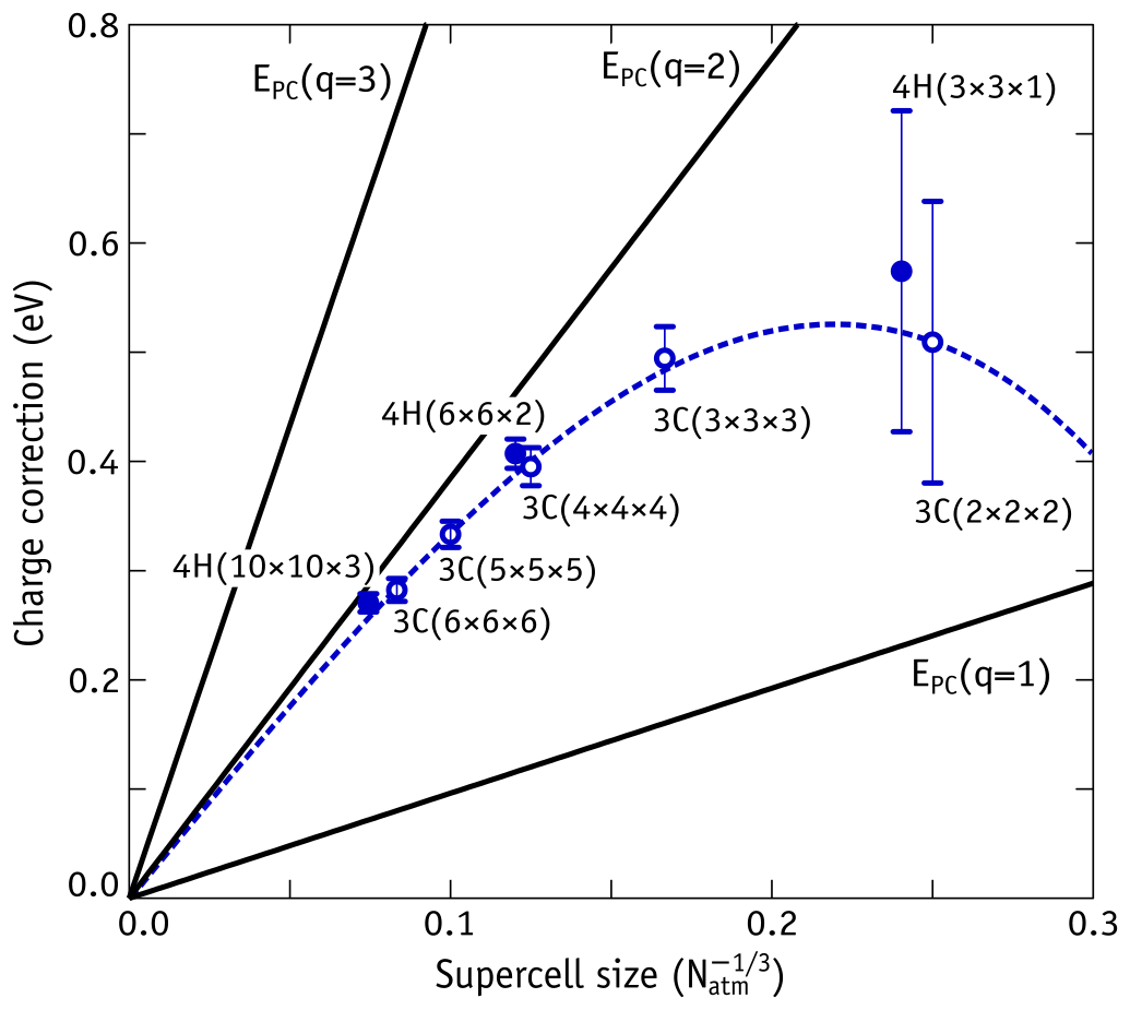
Figure 2 depicts the values of obtained for a defect in -SiC (with symmetry) and -SiC (with symmetry) as a function of the number of atoms in the supercell (). The calculations shown in this particular figure were carried out within PBE-level. The results were essentially the same when using the HSE06 functional. Integer triplets in the figure are scaling factors applied to the lattice vectors of the conventional cell (8 atoms in both polytypes) to obtain the respective supercell. For example, the largest hexagonal cell (-SiC) consisted of atoms, whereas the smallest cubic cell (-SiC) had atoms. can be expanded in a power series of , with the first term and the second term scaling as .Makov and Payne (1995); Castleton et al. (2006) The data were therefore used to fit a function of the form , which is shown by the dashed line. The solid straight lines represent the leading term, , as a function of . It is clear that the simple Madelung (point-like) correction overestimates the spurious Coulomb energy. Also as expected, asymptotically converges to for supercells of infinite size. The error of the Madelung correction is always above the statistical error of obtained from averaging and shown as error bars. In the case of the -SiC supercells (used in this work to study the carbon vacancy), our best estimate for the correction of is eV, whereas for a singly charged vacancy (not shown in the graph) we obtained eV.
For the calculation of formation energies we follow the usual procedure, introduced by Qian, Martin and Chadi.Qian et al. (1988) Here the formation energy of a carbon vacancy is
| (3) |
where is the charge-corrected total energy of the defective supercell as defined above. Besides depending on the charge state , may refer to more than one atomic structure . is the energy of a perfect supercell, is the carbon chemical potential (see below), is the valence band edge and the Fermi energy which may vary within . The upper limit, eV, is the calculated forbidden gap width, here obtained within the delta self-consistent (SCF) method,Hedin and Lundqvist (1970) where eV and eV are ionization potentials of neutral and negatively charged supercells. They are negative as their reference (zero-energy) is ill-defined for a periodic calculation. According to this method , allowing to consistently express the calculated transition levels with respect to both and without having to rely on the experimental band gap.
We note that using the -point for BZ sampling, the eV obtained by the SCF method is 0.25 eV wider than the indirect gap from the Kohn-Sham energies of the highest-occupied and lowest-unoccupied states at and , respectively. This compares with eV and eV from analogous SCF calculations using -centered (simple -point) and -point sampling grids. The -sampled energy coincides with the Kohn-Sham gap simply because of band-folding, which for a -supercell brings the -point into the origin of the BZ. These results indicate that -sampled energy differences (like - and -point calculations) may suffer from insufficient sampling density. This effect is expected to be more severe for energy differences involving the occupation (or emptying) of highly dispersive states. The calculation of is perhaps an extreme case. It involves emptying the top-most valence band and filling the bottom-most conduction band, both showing considerable dispersion amplitudes. On the other hand, for sufficiently large supercells, localized defect states show little dispersion and sampling errors tend to cancel when considering energy differences. This is confirmed by -point, -point and -grid calculations of for the vacancy at the -site, which gives an average value and maximum deviation of eV.
In Eq. 3, represents the energy per carbon atom in the SiC crystal, which is subject to
| (4) |
where the upper and lower bounds represent C-rich and C-poor SiC crystals, which are in equilibrium with standard carbon and silicon phases, respectively. For crystals grown under stoichiometric conditions we have . Here is the heat of formation of SiC estimated as eV, with being the energy per SiC formula unit in a perfect crystal, while and are chemical potentials (energy per atom) of C and Si in diamond and silicon crystals, respectively. The value calculated for is close to eV as obtained from calorimetry measurements.Greenberg et al. (1970)
An important use of Eq. 3 is in locating the value of for which two different charge states, say and , have the same energy, and therefore the same probability to occur. The transition level with respect to the valence band top is found at such that ,
| (5) |
where we distinguish eventual different structures and for charge states and , respectively. It is also useful to calculate transition levels with respect to the conduction band minimum. For that we have,
| (6) |
We also investigated the transformation of VC defects between different structures and also between different symmetry-equivalent alignments. We assume the adiabatic approximation, and the potential energy surface governing the atomic motion was calculated using the climbing-image nudged elastic band (NEB) method.Henkelman et al. (2000) The NEB algorithm allows to find saddle points and minimum energy paths separating known initial and final structures. The method optimizes a number of intermediate structures along the reaction path while maintaining equal spacing between them. This is possible thanks to the introduction of spring forces connecting neighboring structures (the elastic band) and projecting out the component of the force due to the potential perpendicular to the band. The NEB relaxations were carried out within the PBE-level, used 7 intermediate structures, and the forces acting on the atoms were also converged within eV/Å. The initial, final and saddle-point structures (, and , respectively) were used to obtain their respective total energies (, and ) using the HSE06 functional.
III Results
III.1 Ground-state results for the carbon vacancy
We start by reporting on the structural properties of the defect on different charge states. The VC defect was always found to have the lowest energy in low-spin states. We identified four different atomistic configurations, which we label with the letters A (with symmetry), and B, C and D (with symmetry). They are distinguished by the shape of the tetrahedron with volume and with edge lengths connecting Sii-Sij nuclei. Some edges are shorter/longer than others and they are schematically represented by solid/dashed edges, respectively, in the middle of Figure 3. By defining an effective length as the geometric average length of the edges , A-D structures may be defined by simple distortion coordinates with magnitudes,
| (7) | |||||
| (8) | |||||
| (9) | |||||
| (10) |
where elongations have pre-factors that depend on the number of symmetry-equivalent edges. Hence, structure A forms a triangular pyramid with a Si1 apex and a contracted Si base, whereas structures B, C and D form monoclinic tetrahedrons with a mirror plane and mirror-symmetric Si3 and Si4. On these three structures, we found 2, 1 and 3 contracted edges (4, 5 and 3 elongated ones), respectively. Below, we show how these shapes are intimately related to the occupation of the one-electron orbitals.
| A | 0. | 032 | 0. | 032 | 0. | 031 | 0. | 031 | 0. | 626 | 0. | 191 | |
| A* | 0. | 061 | 0. | 061 | 0. | 058 | 0. | 058 | 0. | 140 | 0. | 359 | |
| B | 0. | 117 | 0. | 090 | 0. | 035 | 0. | 093 | 0. | 090 | 0. | 461 | |
| B | 0. | 241 | 0. | 180 | 0. | 139 | 0. | 200 | 0. | 443 | 1. | 079 | |
| C* | 0. | 000 | 0. | 111 | 0. | 112 | 0. | 309 | 0. | 679 | 0. | 747 | |
| D | 0. | 312 | 0. | 267 | 0. | 090 | 0. | 141 | 0. | 716 | 1. | 167 | |
| D | 0. | 233 | 0. | 345 | 0. | 234 | 0. | 359 | 1. | 065 | 1. | 750 | |
| A | 0. | 006 | 0. | 006 | 0. | 006 | 0. | 006 | 0. | 581 | 0. | 036 | |
| A | 0. | 061 | 0. | 061 | 0. | 061 | 0. | 061 | 0. | 196 | 0. | 366 | |
| B* | 0. | 065 | 0. | 088 | 0. | 000 | 0. | 102 | 0. | 132 | 0. | 335 | |
| B | 0. | 229 | 0. | 146 | 0. | 097 | 0. | 256 | 0. | 440 | 0. | 971 | |
| C | 0. | 037 | 0. | 097 | 0. | 068 | 0. | 640 | 0. | 735 | |||
| D* | 0. | 071 | 0. | 194 | -0. | 286 | 0. | 255 | 0. | 703 | 1. | 286 | |
| D | 0. | 220 | 0. | 295 | 0. | 331 | 0. | 292 | 1. | 033 | 1. | 765 | |
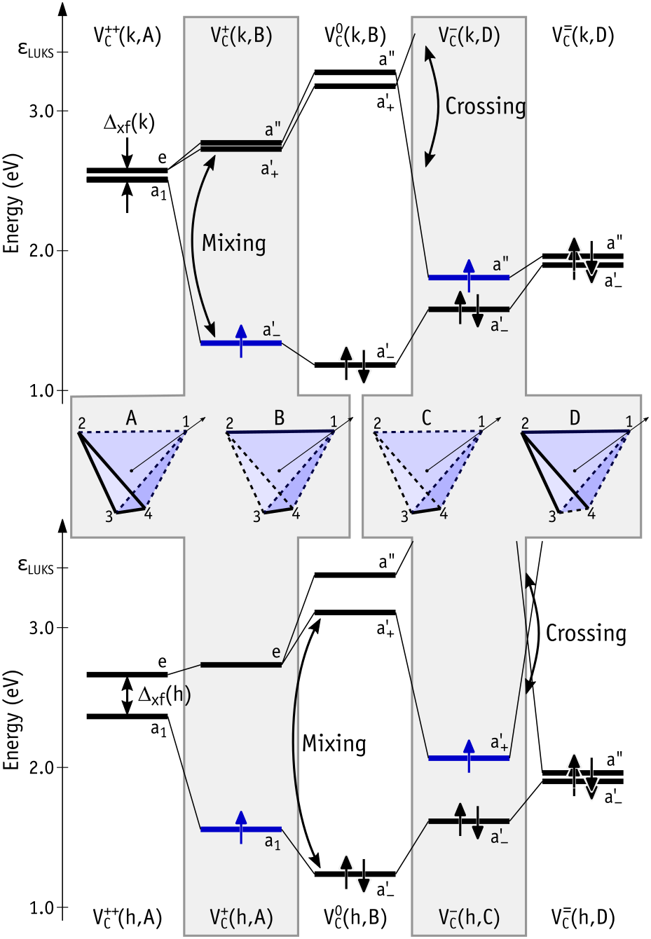
In line with previous works,Zywietz et al. (1999); Bockstedte et al. (2003); Umeda et al. (2004a); Bratus’ et al. (2005); Trinh et al. (2013) we found that V and V defects are trigonal (structure A). Both introduce three empty states deep in the gap, namely a singlet level below a doubly degenerate level (). Their separation, , results from the local crystal field. Figure 3 represents the (hybrid) Kohn-Sham energies of ground-state carbon vacancies as a function of the level occupancy and sub-lattice site. The level energies are reported with respect to the eigenvalue of bulk. To make the interpretation easier, we present a spin-averaged picture, although the filling of levels is represented with upward/downward arrows.
From the eigenvalues we obtain crystal-field energies eV and eV for V and V, respectively. We will show that this site-dependence of the crystal-field confers rather distinct electronic structures on V and V. Table 1 reports the geometrical details regarding the evolution of ground-state structures as we fill in the manifold with electrons. Also included are the results for metastable structures (starred structures). These were only found for charge states and will be discussed in Section III.2. Besides edge elongations , distortion magnitudes and the volume expansion of the vacancy tetrahedron (with respect to the analogous quantity in bulk) are also shown. It is clear that positive charge states are compressive (), while negatively charged ones are tensile (). This is a consequence of the breaking/formation of reconstructed bonds between the four Si radicals edging the vacancy as we respectively remove/add electrons from/to defect states in the gap. For the same reason, distortions () tend to increase in magnitude as we go from V to V. We also note that structures A and B were concurrently found for the positive charge state, whereas structures C and D were found for the negative charge state. This is emphasized in Figure 3 by two shaded regions.
All paramagnetic ground-states differ in their atomic geometries, namely V, V, V and V, and show , , and symmetry, respectively. Inspection of the paramagnetic (highest occupied) one-electron wave-functions allowed us to identify their symmetry and LCAO representations. For the monoclinic structures we have two mirror-symmetric states (see Figure 3), and they are distinguished by and subscripts, standing for low- and high-energy symmetric states. Hence, we found that and for V and V, respectively, while for negative charge states we found and for V and V, respectively. Besides being compatible with the low-temperature EPR and HF data, the above results reproduce earlier density-functional findings.Bockstedte et al. (2003); Umeda et al. (2004a); Bratus’ et al. (2005); Trinh et al. (2013)
We went on and explored the symmetry and wave-function character of non-paramagnetic states. The results are shown in Figure 3. Here we can see that the evolution of the one-electron states, as they become occupied, exhibits a rich picture, which includes crossing and mixing (anti-crossing) features. These effects are responsible for the structural variety that is observed, and to understand them we have to invoke the JT and pJT effects.
III.2 The pseudo-Jahn-Teller effect on the carbon vacancy in -SiC
While the JT theorem asserts the existence of spontaneous symmetry breaking of degenerate electronic states, “the pJT effect is the only source of instability and distortions of high-symmetry configurations of polyatomic systems in non-degenerate states, and it contributes significantly to the instability of degenerate states”.Bersuker (2006)
The pJT effect results in the softening of the adiabatic potential energy surface (APES) around a reference configuration with non-degenerate ground state , and it is due to overlap with excited states via electron-phonon coupling. Should this softening be severe enough to make unstable against atomic distortion towards structure , the curvature of the APES along , which transforms as some irreducible representation , must be negative, . Here is the total energy and the Hamiltonian. It may be shownBersuker (2006, 2013) that the APES softening comes from a negative vibronic contribution to the total curvature , where
| (11) |
is the harmonic curvature and from second-order perturbation theory,
| (12) |
where are off-diagonal vibronic coupling constants between the reference state and excited states with energies and , respectively. represents the force constant resisting the motion of atoms along , whereas is always negative and represents the change in that force constant that results from adapting the electron distribution to one more suited to the new nuclear coordinates,
| (13) |
corresponding to a lower energy . We note that unlike the Jahn-Teller effect, the pJT effect mixes the ground state with excited states to create new bonds and distort the structure. We may actually state that the driving force of the pJT effect is the increase of covalent bonding.Bersuker (2013)
Given that the product , which is the linear term in the expansion of in powers of , is fully symmetric, must also have the same symmetry as . This implies that only excited states which transform as the same irreducible representation of , such that , will lead to non-vanishing coupling constants and contribute to the softening of the APES.Bader and Bandrauk (1968); Pearson (1969, 1986)
Besides the symmetry restrictions imposed to the integral, it is often assumed that only a few low-energy states contribute to due to the increasing energy in denominator of Eq. 12.Bersuker et al. (2002) This premise has justified the replacement of the infinite sums in Eqs. 12 and 13 by a finite set of interacting states, or indeed by a two-level paradigm where a single excited state couples to the ground state via an effective vibronic coupling constant , where is the effective energy separation between the mixing states.Bersuker et al. (2002)
For an accurate description of the pJT effect one would have to solve the many-body Hamiltonian by accounting for dynamic correlation effects (e.g. by means of configuration interaction methods), the electron-phonon coupling would have to be included as well, considering all phonons obeying the above selection rule. Although this has been realized for small molecules using sophisticated quantum chemistry methods,Bersuker (2013) severe approximations have to be made in order to study defects in solids. By using a single-determinant density functional approach we may still arrive at a sufficiently detailed picture of the problem. For instance, García-Fernández and co-workersGarcía-Fernández et al. (2006) were able to explain the off-center displacement of the Fe+ interstitial ion in SrCl2 using local density functional theory. On the contrary, the wave-function-based complete active space second-order perturbation method was applied to the same problem and was unable to reproduce the observations. This failure was attributed to the insufficient number of states included in the active space.García-Fernández et al. (2006) The case of a vacancy in SiC would be much more demanding since the active space spans many ligands to the vacancy site.
We investigated the pJT effect on the VC defect in -SiC, restricting our approach to a single-electron picture. Although we do not have access to important parameters such as accurate many-body gap energies and electron-phonon coupling strengths, we will arrive at an instructive and reasonable picture for the observed distortions. To that end we monitored the change of the one-electron wave-functions and respective energies, while the atomic structure was progressively changed from the high-symmetry VC(A) configuration towards lower-symmetry structures B, C and D with symmetry (). Therefore, according to the selection rules, only fully symmetric states () have to be considered as the source of a pJT effect in VC. The calculations reported within this Subsection were done using the spin-averaged density-functional method within the PBE level. Some tests using a spin-polarized HSE06 functional were also carried out, and apart from the expected differences regarding the energy separation of levels, the conclusions drawn below apply equally.
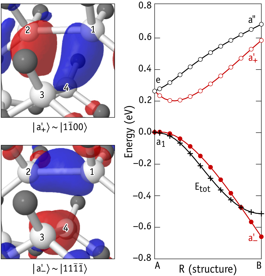
We begin with neutral and positively charged defects. On the left hand side of Figure 4 we depict the highest occupied and lowest unoccupied Kohn-Sham states (HOKS and LUKS, respectively) for the ground state neutral vacancy at the site, V. Both HOKS and LUKS transform according to the irreducible representation of the point group, so we differentiate them by their energy order, i.e. the one with lower energy is referred to as while the higher energy state is . If we consider all three states in the gap, the electronic structure of V is , where the number of electrons on a specific orbital is superscripted. Comparing the ground state in Figure 4 with from V shown in Figure 1(b), it is evident that the lower symmetry state increases the covalent bonding between all four atoms, and that leads to shorter Si1-Si2 and Si3-Si4 distances in structure B. Furthermore, considering that V is a non-degenerate ground state (), we conclude that the states exhibited in Figure 4 must result from a pJT effect.
On the right hand side of Figure 4 we find an electronic structure diagram, showing how the three gap states develop between the trigonal V state with electronic configuration and the monoclinic V state with electronic configuration . Energies of filled and empty states are represented with closed and open symbols, respectively. The same graph also shows the total energy change as crosses, from which we conclude that the high-symmetry configuration A is unstable against relaxation to B. The corresponding pseudo-Jahn-Teller relaxation energy, eV, relates to the added covalence. The distortion transforms as within (couples to electronic states), and consists in the compression of Si1-Si2 and Si3-Si4 distances, along with the expansion of the remaining tetrahedron edges (see Table 1). Looking again at Figure 1(b), it becomes evident that when subject to a distortion, the state , which transforms as within and shows a strong anti-bonding character between Si1-Si2, should raise in energy, while the doublet component , also transforming as within and showing a bonding character between Si3-Si4, is expected to be stabilized and lower its energy. This opposite coupling leads to the typical pJT anti-crossing pattern shown in Figure 4 for and states.
We may estimate the relative contribution (mixing) from and states to the pJT distorted and states using our simple LCAO model. From inspection of Figures 1(b) and 4, and considering normalization coefficients and we arrive at,
| (14) | |||||
| (15) |
Like the isosurfaces shown in Figure 4, the ground state in Eq. 15 has the same phase (bonding character) on Si1,2 and Si3,4 atom pairs, and that mostly comes from . Conversely, is an anti-bonding state between Si1,2 atoms with vanishing amplitude on Si3,4, and most of its character comes from . The above discussion and conclusions can be applied to the neutral vacancy at the hexagonal site as well. However, the stronger crystal-field splitting leads to a larger energy gap , and therefore to a weaker mixing effect.
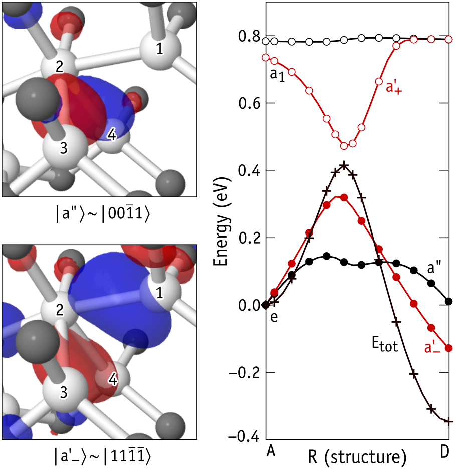
For positively charged vacancies on both - and -sites, the shape of the electronic structure diagrams (and wave-functions) were found to be close to those of Figure 4, although for V(A) and V(B) indicated that these were both minima in the APES of and sites. From Table 1 we see that the distortion magnitudes of positively charged defects are considerably smaller than in neutral defects. We may conclude that the pJT coupling is weaker for V(B), particularly in the hexagonal site where the crystal field is stronger. Here, the V state with two (weak) Si-Si bonds sharing a single electron, is essentially degenerate with the V state . Their energy difference is estimated below meV.
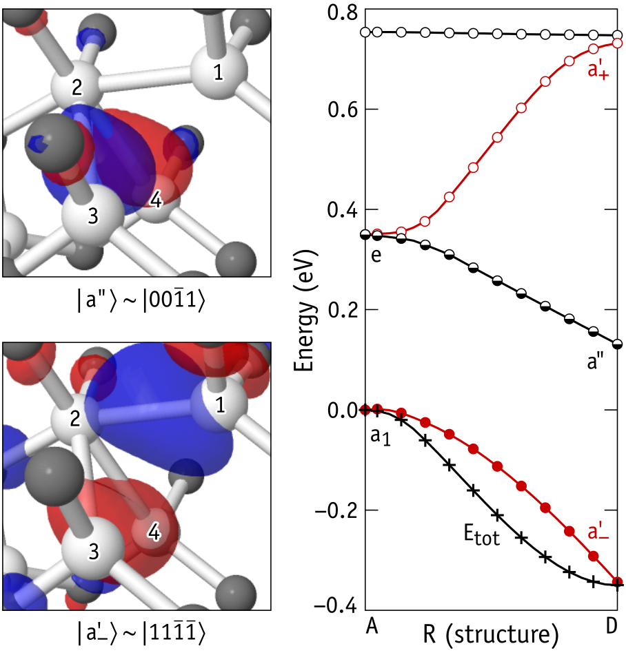
For the negatively charged vacancies, the picture is dramatically different. We start by analyzing the double negative charge state, where structure D was found to be the most stable for both and sites. For the trigonal structure on the -site (the structure was relaxed by symmetrizing the forces), we found that the state with spin-0 was less stable than the spin-1 configuration by 0.20 eV, but the latter was still metastable by 0.15 eV when compared to the non-degenerate ground state. On the left hand side of Figure 5 we depict the (fully occupied) levels found within the gap for V. Comparing these wave-functions with those shown in Figure 1(b) for the symmetric structure, we realize that although the HOKS state of structure D is rather similar to from the trigonal structure, the does not find a good match, although one could suggest some resemblance with . Considering that (i) V is non-degenerate, and therefore not vulnerable to a JT distortion, and (ii) that is a mixed state with a major contribution from , the wave-functions exhibited in Figure 5 must result from a pJT effect. In fact, looking at the right hand side of Figure 5, it becomes evident that has been converted into under distortion , whereas (derived from ) seems to have merged into the conduction band (uppermost state close to 0.8 eV) before the ground state was attained.
In fact, shows bonding character for Si1-Si2 and Si3-Si4 pairs, and can be described approximately as like in Eq. 15. It becomes now clear that structure D results from structure B (occupation of leads to the shortening of Si1-Si2 and Si3-Si4 distances) combined with the occupation of , which is anti-bonding on Si3-Si4. The result is a tetrahedral structure with short Si1-Si2, Si2-Si3 and Si2-Si4 edges. We finally note that V shows a similar behavior to V, with the metastability of the trigonal structure by 0.5 eV being worthy of mentioning.
For the singly negative charge states, we found that imposing structure A to the defect (symmetry-constrained relaxation) the self-consistent electronic structure showed a occupation (with spin-1/2) for both sites and . In this case both trigonal structures are vulnerable to the JT effect. Monoclinic distortions applied to V and V ground states were found to release 0.39 eV and 0.36 eV, respectively. The two highest occupied states of V and their change along the A-D path on the APES are depicted in Figure 6. We can conclude that despite showing occupied and states like in the double minus charge state (and hence showing a similar structure), the diagram on the right side of the figure is rather different than that shown in Figure 5. The high-symmetry configuration V is now unstable due to the Jahn-Teller effect. Interestingly, the splitting order of the -state favors the stabilization of the nodal state with higher kinetic-energy (under the monoclinic field). We will come back to this issue in Section IV.
On the site we found that the JT splitting order of the -state of V involves the raising in energy of the anti-symmetric state under the monoclinic distortion . Unlike for the cubic site, we have now a occupation scheme. This difference is attributed to the relatively stronger crystal field separating and states of the symmetric configuration in V, and consequently to a weaker coupling between and states. The resulting structure C is therefore based on structure B (due to the occupation of ), but shows an elongated Si1-Si2 distance due to occupation of the anti-bonding state (see Figure 4).
III.3 Dynamical effects
We calculated minimum energy barriers separating different distorted structures along the APES using the NEB method. Table 2 reports the most favorable forward () and backward () barriers, between several initial and final structures. The sub-lattice site and charge state are indicated as pairs on the first column. Two types of mechanisms were considered, namely rotations (R) and transformations (T). A rotation involves a 120∘ rotation of the mirror plane of monoclinic structures (B, C and D), which are converted into symmetry-equivalent final states (B’, C’ and D’). A transformation involves a structural change to an inequivalent state (), which may as well include a change in the direction of the symmetry plane. In that case, they are also indicated by primed final states.
| Type | ||||||
|---|---|---|---|---|---|---|
| R | 0.05 | |||||
| T | 0.12 | 0.04 | 0.08 | |||
| R | 0.41 | |||||
| R | 0.15 | |||||
| R | 0.17 | |||||
| T | 0.14 | 0.12 | 0.02 | |||
| T | 0.06 | 0.04 | 0.02 | |||
| R | 0.28 | |||||
| R | 0.02 | |||||
| T | 0.02 | 0.02 | 0.01 | |||
| R | 0.30 | |||||
| R | 0.08 | |||||
| R | 0.05 | |||||
| T | 0.24 | 0.10 | 0.14 | |||
| T | 0.17 | 0.03 | 0.14 | |||
| R | 0.25 |
For V we have two low energy structures, namely A (metastable) and B (ground state). The simple rotation mechanism involves surmounting a small 0.05 eV barrier. On the other hand, the transformation has a 0.12 eV barrier, and so it has the alternative combined rotation mechanism. For V, structure A was found to be more stable than B by less than 1 meV, so we consider them essentially degenerate. Both rotation of the mirror plane in as well as the transformation involve overcoming a minute barrier of 0.02 eV. Hence, for the -site, the rotation between (symmetric) equivalent B structures should be the first dynamic effect to take place as the temperature is raised from 5 K. On the other hand, for the -site it appears that even at very low temperatures, V defects may cohabit with V states, with the later being able to hop between different alignments.
V was found to have low energy in structures C (metastable) and D (ground state), which are separated by only 0.02 eV. Simple rotation mechanisms and involve barriers of 0.17 eV and 0.15 eV, respectively. The in-plane transformation also has a comparable barrier of 0.14 eV. On the other hand, the off-plane transformation is the most favorable mechanism with a barrier of 0.06 eV. These results suggest that the lowest-temperature dynamic mechanism involving atomic motion in V should involve a sequential transformation. For the -site, the negatively charged vacancy is also stable for structures C and D, although D is now metastable by 0.14 eV. For this reason, in-plane and off-plane transformations involve relatively high barriers of 0.24 eV and 0.17 eV, respectively, whereas simple rotation mechanisms and have only to overcome 0.08 eV and 0.05 eV barriers. This suggests that at low temperatures, the first thermally-activated dynamic effect will involve a simple rotations.
We note that several of the above figures, like or barriers are rather small. They are close to the error bar of the current methodology and should be considered with caution. However, their relative magnitudes are in line with the lowest-temperature dynamic processes observed in the EPR main signals and hyperfines. Accordingly, raising the temperature above 50 K, the pattern of the V main line is converted from monoclinic to trigonal. This is assigned to a rotation with a calculated 0.05 eV barrier (estimated experimentally as 14 meV). Above 10 K, the main EPR signal of V and related HFs suffer a progressive change. Such low temperature is consistent with the minute (0.02 eV) transformation barrier. Raising the temperature above 40 K, the V signal shows a series of different transformations, which can be explained by a sequence of transformations with a 0.06 eV barrier. Finally, for V, the measurements indicate that the first thermally activated process is limited by an estimated barrier of 20 meV at about 60-70 K, also in line with our calculated barrier of 0.08 eV for the realignment.
The neutral charge states (both at and sites) only have one stable structure and only rotations are possible. For these mechanisms we found relatively high barriers of about 0.4 eV and 0.3 eV for V and V, respectively. For double negatively charged defects we also found relatively static defects. Here the ground state is the D structure for V and V, with respective metastable C structures at 0.26 eV and 0.22 eV above D. Their respective rotation mechanism were found to be limited by 0.28 eV and 0.25 eV high barriers.
III.4 Electrical levels and metastability
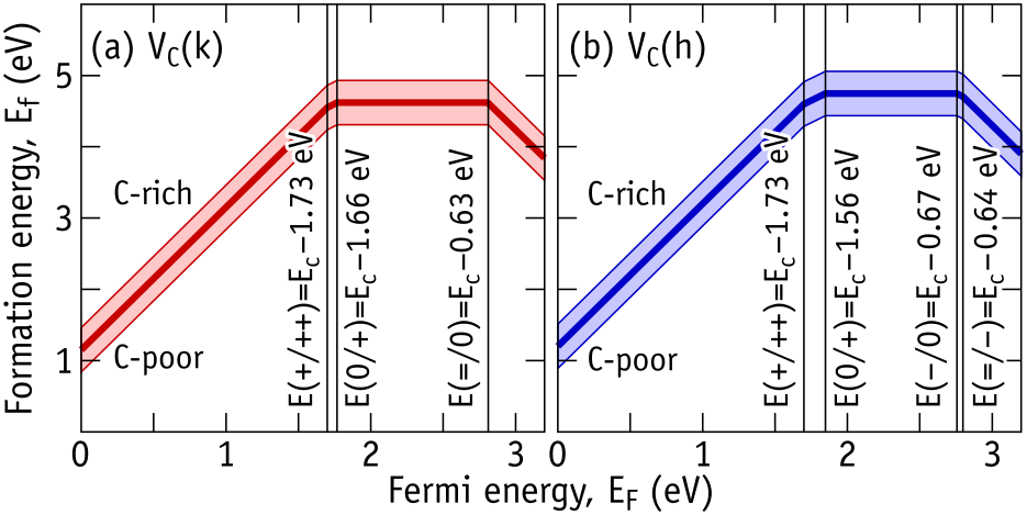
The formation energy of VC defects was calculated using Eq. 3. The results are depicted in Figure 7, where each diagram includes formation energies under C-rich, stoichiometric and C-poor growth-conditions. In agreement with Ref. Hornos et al., 2011, the formation energy of neutral V and V defects in C-rich material is 4.93 eV and 5.06 eV, respectively, whereas in C-poor -SiC these quantities are off-set by eV to 4.31 eV and 4.44 eV, respectively. For stoichiometric conditions values are mid-way between C-rich and C-poor figures. The C-rich results agree very well with the formation enthalpy of 4.8-5.0 eV measured from samples grown under analogous conditions.Ayedh et al. (2014, 2015)
Also like in Ref. Hornos et al., 2011, we only find negative- behavior ( eV) for the acceptor levels of V, i.e. we find a eV occupancy level, with V being metastable irrespectively of the position of the Fermi energy. The acceptors of V are located close to eV and separated by a rather small but positive eV. Donor levels are estimated between eV and eV, with and levels being separated by positive eV and eV for V and V defects, respectively.
We may conclude that both acceptor and donor levels are very close to the DLTS measurements of Z1/2 at eV and EH6/7 at about eV, respectively, supporting the assignment of both signals to the carbon vacancy. The relative magnitude of the calculated -values can be connected with the amount of excitation, namely the illumination frequency/intensity and sample temperature needed for the observation of the paramagnetic states. Accordingly, V is predicted to have eV and its EPR signal could only be seen in highly-doped n-type material under illumination,Son et al. (2012) traces of the V signal, with calculated eV, were detected in darkness at K,Son et al. (2012) both EPR signals of V, with calculated eV, could be detected in darkness even at temperatures as low as K.Umeda et al. (2004a) This trend agrees with our calculated ordering of values, so that paramagnetic states with smaller (and negative) values have lower probability to occur because of concurrent formation of energetically favorable diamagnetic states.
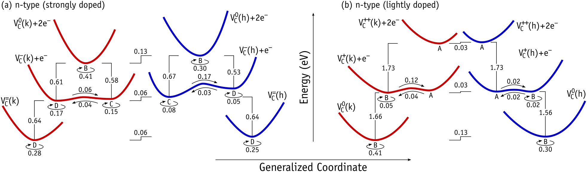
While singly negative charge states need some sort of excitation (optical or thermal) to be observed, which is consistent with a negative- behavior, the EPR data for positively charged vacancies seems actually characteristic of a positive- ordering of levels. Otherwise, how could we explain the observation of both V and V at K without illumination?Umeda et al. (2004a) To investigate this issue we need to have a more detailed view of the electronic/atomic transitions that take place during DLTS measurements. Combining the relative energies of V states with the calculated rotation/transformation barriers and levels, we arrived at the configuration coordinate diagram of Figure 8, which describes several electronic emission processes that take place during electrical measurements in n-type material.
Figure 8(a) represents electron emission energies from negative charge states in highly doped n-type material. Here, the Fermi level is located above the acceptor levels. Figure 8(b) represents electron emission energies from donor states in lightly doped n-type material. The Fermi level is now between donor and acceptor levels. Energies on each inset [(a) and (b)] refer to different scales, and the curvature of the potential curves is arbitrary.
We start by analyzing electron emissions in highly doped material from double negatively charge vacancies on the -site. In a DLTS measurement, under a zero-bias filling pulse, all V electron traps will be filled with electrons and vacancies will be found in the V state. Around room temperature under reverse-bias,Hemmingsson et al. (1997) after a first electron emission with binding energy calculated as 0.64 eV, a second emission with lower energy (0.61 eV) will follow immediately, and the defect will end up in the neutral charge state. The reason for the negative- behavior of the V acceptor sequence is the strong relaxation to structure B after the second emission.
On the hexagonal site, the electron binding energy of V is 0.64 eV considering a transition between ground states, . The second emission from V has a slightly larger binding energy of 0.67 eV, corresponding to a small but positive- previously shown in Figure 7(b). This discrepancy with the DLTS data could indicate that the stability of V is overestimated, or alternatively, the stability of V is underestimated.
It is possible that the conversion between C and D configurations could play a role during electron emission. For instance, the calculated energy barrier between V and V is 0.06 eV, which should be compared with 0.02 eV from analysis of the thermally activated motional effects observed in EPR.Umeda et al. (2005) Since atomic rotations/transformations occur on a much faster time-scale than electronic transitions, we cannot exclude the possibility that at the temperature of the DLTS measurements, emission from V could initiate from metastable states, thus leading to an effective smaller second ionization.
In as-grown material, where vacancies are in equilibrium conditions, Ref. Hemmingsson et al., 1997 reports a Z peak which was about twice the intensity of Z. This contrasts with irradiated material where Z and Z show up with about the same magnitude. Since carbon vacancies are invariably more stable in the cubic site (by about 0.06 eV in n-type SiC as shown in Figure 8), we attribute Z2 and Z1 signals to V and V, respectively. A 1:2 intensity ratio corresponds to a concentration ratio under equilibrium conditions at K. This assignment is also consistent with a previous connection between Z1 and V by photo-EPR,Son et al. (2012) it is supported by the lower calculated -value for the acceptor levels of V [when compared to V], and it agrees with the calculated deeper transition for V than V. We finally note that the calculated eV between and acceptors of V must not be far from the true value. This value is consistent with the observation of the V EPR signal at 100 K (without illumination) and its photo-ionization with photon energies eV below the band-gap threshold.Son et al. (2012) In contrast, the analogous photo-ionization for the cubic vacancy could not be observed, most probably because is more negative and the most favorable V defects are diamagnetic.
The calculated donor levels are also represented in Figure 8(b). Although first and second electron binding energies, i.e. and transitions, are close for both sub-lattice sites, they do not form a negative- sequence. The -value for is eV, while for the -site eV. These results are in partial agreement with the data reported by Booker et al.Booker et al. (2016), where eV for EH7 and eV for EH6, obviously favoring the assignment of V and V to EH7 and EH6, respectively. Again, we may use the relative stability of and to identify the sub-lattice sites of EH7 and EH6 signals. In as-grown material and electron irradiated samples subject to high temperature anneals, the EH6:EH7 ratio was found to be about 4:5,Danno and Kimoto (2006) suggesting that EH7 is more stable. The relative energies in Figure 8(b), confirm that EH6 and EH7 should therefore be connected toV and V, respectively.
Of course there is some degree of uncertainty in the calculated magnitudes (and sign) of the -values. Within the present level of theory, electronic levels are usually affected by error bars of about eV due to spurious (strain, Coulomb or dispersive) periodic interactions. However, as we will point out in the next Section, there is further experimental evidence for a positive- ordering of donor transitions.
IV Discussion
We start by addressing the strong temperature dependence of the EPR data related to V. The V defect in -SiC has the properties of a pJT distorted structure in the weak-coupling regime, where the pseudo-Jahn-Teller relaxation energy is much smaller than the Debye frequency, .Bersuker (2006) For the case of -SiC we have meV.Slack (1964) We note that the vibronic softening constant, as it is described in Eq. 12, only accounts for a single distortion mode. However, for an accurate account of the pJT vibronic details of a defect in a crystal, a continuum of fundamental and excited vibrational modes would have to be included in the summation. Since this is not practical, we leave a qualitative description supported on the agreement between adiabatic calculations and the measurements. Hence, for temperatures approaching 0 K, all zero-phonon vibrations obeying the selection rules will contribute to the vibronic force constant . If this contribution is not strong enough to produce a negative curvature of the APES at , the vacancy will preserve the state. This could be the case for V since there is good agreement between the magnitude of the low- hyperfines shouldering the EI6 EPR signal and those calculated for V.Bockstedte et al. (2003); Umeda et al. (2004a) For instance, at K the Si1 HF components parallel and perpendicular to the crystallographic -axis were measured as MHz and and MHz, respectively.Umeda et al. (2004b) These are to be compared with MHz and and MHz calculated for V.Bockstedte et al. (2003) With increasing temperature, additional phonon modes are populated, and becomes more negative. Should , the V state will be lower in energy and the observed HFs should be converted to those of the monoclinic defect. The calculations from Ref. Bockstedte et al., 2003 anticipate that this transformation would lead to a Si1 HF splitting with MHz and MHz, which would explain the strong and progressive decrease of the observed HF data to MHz and MHz at K.Umeda et al. (2004b)
The observed trigonal pattern for the EI6 main signal and related hyperfines between 5 K and room-temperature can also be explained based on dynamic arguments. Around the HF signals arise from the state. This static trigonal state accounts for the observed % localization of the paramagnetic wave function on Si1.Umeda et al. (2004b) On the other hand, at higher temperatures the distorted state is expected to quickly hop between all three equivalent states , and . Our calculated hopping barrier of 0.02 eV is compatible with this behavior. Since the three states lead to approximately the same spin-density amplitude and shape on all four Si radicals, the result is the observation of two trigonal HF signals. One of them corresponds to Si1, while the other represents a shell of the three Si atoms, also explaining the observed 1:3 amplitude ratio.Umeda et al. (2004b)
The complex temperature-dependence of the V EPR signal and related hyperfine peaks can also be discussed with help of dynamic arguments. Below K the EPR data shows a symmetric defect with one pair of HF shoulders due to mirror-symmetric Si3,4 radicals. This is consistent with the static D-structure with paramagnetic ground state .Trinh et al. (2013) Increasing the temperature above 40 K leads to the quenching of the Si3,4 HF signal and the angular dependence of the main signal acquires a trigonal shape. Based on the energy difference between V and V (0.02 eV), as well as on the calculated rotation and transformation barriers from Table 2 and Figure 8, we suggest that this effect is connected to the off-plane transformation, which is limited by a barrier estimated as eV. Such a sequence effectively leads to the alternation between structures C and D and to the rotation of the mirror plane of the defect. This mechanism translates into alternate transitions between symmetry-equivalent and conjugate states from structures D and C, respectively. The amplitude of the spin-density on the basal radicals becomes intermittent, explaining the disappearance of these HFs from the V spectrum at K. Above K, new trigonal Si1 and Si HFs appear in the EPR spectrum, which are assigned to the combined thermally activated population and rotation of both V and V states.Trinh et al. (2013) However, this argument is incompatible with the above referred localization intermittency which is expected to work above 80 K as well. We note that unlike in of V, the symmetry of the state of V does not impose zero amplitude of the wave function at any of the Si nuclei. The spin-density on Si3 and Si4 is actually small but not zero (see Figure 4). We suggest that for K the V HFs are quenched due to intermittency effects, while V becomes populated and its HF-related features increase in the spectrum. During the thermally activated motion of V, the Si nuclei in the basal plane always contribute with a non-zero hyperfine interaction. This could explain the appearance of the weak and broad Si trigonal HF at about 80 K. V with filling order is expected to show a temperature-dependent pJT effect due increasing coupling between states. This would lead to the stabilization of this state, making it consistent with the strong temperature dependence of the Si1 HF axial component, which increases from 28 MHz at 60 K to 103 MHz at 140 K.Trinh et al. (2013)
An identical argument can applied to V, which adopts the ground state structure C. In this case, structure D is metastable by 0.14 eV, the lowest transformation barrier is 0.17 eV and V does not appear in the spectrum. Below K the V state is static () with two inequivalent HFs on Si1 and Si2 on the symmetry plane. Above K the available thermal energy promotes the rotation mechanism (with calculated barrier of 0.08 eV), and the spin-density intermittency on Si nuclei results in the observation of a single Si1 axial HF. This was explained in Ref. Trinh et al., 2013. Increasing further the temperature above 120 K, led to the appearance of a trigonal Si HF signal, which is in conflict with the intermittency argument. Again, we suggest that raising the temperature also increases the magnitude of the vibronic term for structure C, and that increases the amplitude of the wave function on Si3 and Si4 by further increasing the contribution to . The result is a dynamic state with amplitude on all Si radicals, and a reconciliation of the model with the observations.
The reason for V showing a nodal () ground state, as opposed to V which is a symmetric ground state (), is also due to the weaker crystal-field on site . As depicted in Figure 3, for V the Coulomb interaction between and states causes a crossing of levels between the neutral and the single negatively charged states, and that results in a more stable filling order. Also in Figure 3, it is evident that the stabilization of the filling on the -site indicates that the repulsion between symmetric states is weaker. Hence, the crossing effect observed in V, is now obtained for the double negative charge state in V.
Finally, we would like to underline a fundamental issue regarding the assignment of EH6/7 to the superposition of negative- double donors from V and V.Booker et al. (2016) If that was indeed the case, the peak amplitude of EH6/7 would have to match that of Z1/2, and that is usually not observed by DLTS. In fact, it is widely documented that EH6/7 has a smaller amplitude than Z1/2, irrespective of the sample history, including as-grown, irradiated/implanted plus annealing and thermal processed (see for example Refs. Danno and Kimoto, 2006; Wong-Leung and Svensson, 2008; Alfieri and Kimoto, 2013; Ayedh et al., 2014). This led the authors from Ref. Ayedh et al., 2014 to the suggestion that EH6/7 is a single donor transition. Our calculations are consistent with a broad EH6/7 signal made of closely spaced positive- ordered double donor levels of the vacancy in different sub-lattice sites. Further support for the positive-U sequence of donor levels come from the relative formation energies of VC for different charge states. From these figures we can estimate the fraction of positively charged vacancies, (with respect to total amount of VC defects) when the Fermi level is located halfway between the and levels,
| (16) |
which for a negative- center means that the Fermi level is locked at the transition. Equation 16 neglects the formation of negatively charged vacancies, it assumes that V, V, and V states are in thermal equilibrium at temperature , and kB is the Boltzmann constant. Hence, at K and considering eV reported for EH7 by Booker et al.Booker et al. (2016) we arrive at , essentially telling us that under these conditions all vacancies would be EPR-inactive. This strongly indicates that the real -value of EH7defect should be positive. Analogous conclusions would be drawn for EH6.
V Conclusions
We report on density functional calculations of the electronic and dynamic properties of the carbon vacancy in -SiC using semi-local and hybrid functionals. The defect exhibits a rich catalogue of structures that depend on the sub-lattice site and charge state. Their occurrence is rationalized on the basis of several effects, namely the character of the occupied one-electron states, the site-dependence of the crystal-field, and the magnitude of the pseudo-Jahn-Teller effect. Diamagnetic states show either strong or no pseudo-Jahn-Teller effect and possess a relatively deep potential energy surface. They display stable ground state structures A, B and D for charge states , and , respectively, no matter their sub-lattice site. Conversely, paramagnetic charge states and suffer from weak pseudo-Jahn-Teller distortions. Here, ground states are respectively B and D for the -site, whereas they are respectively A and C for the -site. This structural variety essentially arises from the stronger crystal-field on the -site that stabilizes electronic states polarized along the main axis. Also for the paramagnetic states, and depending on the strength of the vibronic coupling within the pseudo-Jahn-Teller effect, metastable structures play an important role in the behavior of the vacancy as a function of temperature. For charge states and , structures A and C are metastable in the sub-lattice site , respectively, while structures B and D are metastable in the sub-lattice site .
Mechanisms for the transformation between these structures, as well as for the rotation of the mirror plane for monoclinic structures (B, C, and D) were calculated and discussed in the light of the temperature-dependence of the EPR data. From the total energies, electrical levels and nudged elastic band calculations we constructed a configuration coordinate diagram which considers electronic transitions, as well as structure rotations and transformations between the relevant configurations.
Regarding the electrical activity, our results support the assignment of Z1/2 and EH6/7 DLTS signals to the acceptor and donor transitions of the carbon vacancy. We were able to attribute a sub-lattice site to each component of the DLTS signals based on (i) the correlation between the relative magnitudes of the calculated and measured -values, and (ii) the correlation between the site-dependent formation energies and the relative intensity of the DLTS peaks in as-grown material. Accordingly, we support the assignment of Z1 and Z2 DLTS peaks to two-electron cascade emissions from V and V defects, respectively. We were able to apply analogous arguments to the donor transitions. In this case we assign EH6 and EH7 peaks to electron emissions from V and V defects, respectively. Our results favor a positive- ordering for the donor transitions in both sub-lattice sites. Hence, each peak should result from and transitions with very close emissions rates. Although this is at variance with recent electrical measurements,Booker et al. (2016) they are consistent with the low-temperature EPR data acquired in darkness.
Acknowledgements
We would like to thank Prof. Bengt Svensson for providing fruitful comments and criticisms. This work was jointly supported by the Science for Peace and Security NATO Program through project SPS 985215, and by the Fundação para a Ciência e a Tecnologia (FCT) through project UID/CTM/50025/2013. The authors would like to further acknowledge the computer resources provided by the Swedish National Infrastructure for Computing (SNIC) at PDC.
References
- Park (1998) Y. S. Park, ed., SiC Materials and Devices, 1st ed., Semiconductors and Semimetals, Vol. 52 (Academic Press, San Diego, 1998).
- Kimoto and Cooper (2014) T. Kimoto and J. A. Cooper, eds., Fundamentals of Silicon Carbide Technology (John Wiley & Sons Singapore Pte. Ltd, 2014).
- Iwamoto and Svensson (2015) N. Iwamoto and B. G. Svensson, “Defects in semiconductors,” (Elsevier, Waltham, USA, 2015) Chap. 10, pp. 369–407.
- Nipoti et al. (2015) R. Nipoti, U. Grossner, and G. Alfieri, in Silicon Carbide and Related Materials 2014, Materials Science Forum, Vol. 821 (Trans Tech Publications, 2015) pp. 381–386.
- Kimoto et al. (1995) T. Kimoto, A. Itoh, H. Matsunami, S. Sridhara, L. L. Clemen, R. P. Devaty, W. J. Choyke, T. Dalibor, C. Peppermüller, and G. Pensl, Applied Physics Letters 67, 2833 (1995).
- Hemmingsson et al. (1997) C. Hemmingsson, N. T. Son, O. Kordina, J. P. Bergman, E. Janzén, J. L. Lindström, S. Savage, and N. Nordell, Journal of Applied Physics 81, 6155 (1997).
- Hiyoshi and Kimoto (2009) T. Hiyoshi and T. Kimoto, Applied Physics Express 2, 041101 (2009).
- Hemmingsson et al. (1998) C. G. Hemmingsson, N. T. Son, A. Ellison, J. Zhang, and E. Janzén, Phys. Rev. B 58, R10119 (1998).
- Hemmingsson et al. (1999) C. G. Hemmingsson, N. T. Son, A. Ellison, J. Zhang, and E. Janzén, Phys. Rev. B 59, 7768 (1999).
- Son et al. (2012) N. T. Son, X. T. Trinh, L. S. Løvlie, B. G. Svensson, K. Kawahara, J. Suda, T. Kimoto, T. Umeda, J. Isoya, T. Makino, T. Ohshima, and E. Janzén, Phys. Rev. Lett. 109, 187603 (2012).
- Watkins (1984) G. D. Watkins, “Negative- properties for defects in solids,” in Advances in Solid State Physics, edited by P. Grosse (Springer Berlin Heidelberg, Berlin, Heidelberg, 1984) pp. 163–189.
- Dmowski (1990) K. Dmowski, Review of Scientific Instruments 61, 1319 (1990).
- Aboelfotoh and Doyle (1999) M. O. Aboelfotoh and J. P. Doyle, Phys. Rev. B 59, 10823 (1999).
- Koizumi et al. (2013) A. Koizumi, V. P. Markevich, N. Iwamoto, S. Sasaki, T. Ohshima, K. Kojima, T. Kimoto, K. Uchida, S. Nozaki, B. Hamilton, and A. R. Peaker, Applied Physics Letters 102, 032104 (2013).
- Ayedh et al. (2014) H. M. Ayedh, V. Bobal, R. Nipoti, A. Hallén, and B. G. Svensson, Journal of Applied Physics 115, 012005 (2014).
- Danno and Kimoto (2006) K. Danno and T. Kimoto, Japanese Journal of Applied Physics 45, L285 (2006).
- Booker et al. (2016) I. D. Booker, E. Janzén, N. T. Son, J. Hassan, P. Stenberg, and E. Ö. Sveinbjörnsson, Journal of Applied Physics 119, 235703 (2016).
- Storasta et al. (2004) L. Storasta, J. P. Bergman, E. Janzén, A. Henry, and J. Lu, Journal of Applied Physics 96, 4909 (2004).
- Reshanov et al. (2007) S. A. Reshanov, G. Pensl, K. Danno, T. Kimoto, S. Hishiki, T. Ohshima, H. Itoh, F. Yan, R. P. Devaty, and W. J. Choyke, Journal of Applied Physics 102, 113702 (2007).
- Zippelius et al. (2011) B. Zippelius, A. Glas, H. B. Weber, G. Pensl, T. Kimoto, and M. Krieger, Materials Science Forum 717-720, 251 (2011).
- Alfieri and Kimoto (2013) G. Alfieri and T. Kimoto, Applied Physics Letters 102, 152108 (2013).
- Bockstedte et al. (2003) M. Bockstedte, M. Heid, and O. Pankratov, Phys. Rev. B 67, 193102 (2003).
- Umeda et al. (2004a) T. Umeda, J. Isoya, N. Morishita, T. Ohshima, T. Kamiya, A. Gali, P. Deák, N. T. Son, and E. Janzén, Phys. Rev. B 70, 235212 (2004a).
- Son et al. (2001) N. T. Son, P. N. Hai, and E. Janzén, Phys. Rev. B 63, 201201 (2001).
- Zvanut and Konovalov (2002) M. E. Zvanut and V. V. Konovalov, Applied Physics Letters 80, 410 (2002).
- Konovalov et al. (2003) V. V. Konovalov, M. E. Zvanut, and J. van Tol, Phys. Rev. B 68, 012102 (2003).
- Umeda et al. (2004b) T. Umeda, J. Isoya, N. Morishita, T. Ohshima, and T. Kamiya, Phys. Rev. B 69, 121201 (2004b).
- Bratus’ et al. (2005) V. Y. Bratus’, T. T. Petrenko, S. M. Okulov, and T. L. Petrenko, Phys. Rev. B 71, 125202 (2005).
- Umeda et al. (2005) T. Umeda, Y. Ishitsuka, J. Isoya, N. T. Son, E. Janzén, N. Morishita, T. Ohshima, H. Itoh, and A. Gali, Phys. Rev. B 71, 193202 (2005).
- Trinh et al. (2013) X. T. Trinh, K. Szász, T. Hornos, K. Kawahara, J. Suda, T. Kimoto, A. Gali, E. Janzén, and N. T. Son, Phys. Rev. B 88, 235209 (2013).
- Zywietz et al. (1999) A. Zywietz, J. Furthmüller, and F. Bechstedt, Phys. Rev. B 59, 15166 (1999).
- Kawahara et al. (2013) K. Kawahara, X. T. Trinh, N. T. Son, E. Janzén, J. Suda, and T. Kimoto, Applied Physics Letters 102, 112106 (2013).
- Kawahara et al. (2014) K. Kawahara, X. T. Trinh, N. T. Son, E. Janzén, J. Suda, and T. Kimoto, Journal of Applied Physics 115, 143705 (2014).
- Bockstedte et al. (2010) M. Bockstedte, A. Marini, O. Pankratov, and A. Rubio, Phys. Rev. Lett. 105, 026401 (2010).
- Hornos et al. (2011) T. Hornos, A. Gali, and B. G. Svensson, Materials Science Forum 679-680, 261 (2011).
- Kresse and Hafner (1993) G. Kresse and J. Hafner, Phys. Rev. B 47, 558 (1993).
- Kresse and Hafner (1994) G. Kresse and J. Hafner, Phys. Rev. B 49, 14251 (1994).
- Kresse and Furthmüller (1996a) G. Kresse and J. Furthmüller, Computational Materials Science 6, 15 (1996a).
- Kresse and Furthmüller (1996b) G. Kresse and J. Furthmüller, Phys. Rev. B 54, 11169 (1996b).
- Blöchl (1994) P. E. Blöchl, Phys. Rev. B 50, 17953 (1994).
- Heyd et al. (2003) J. Heyd, G. E. Scuseria, and M. Ernzerhof, The Journal of Chemical Physics 118, 8207 (2003).
- Krukau et al. (2006) A. V. Krukau, O. A. Vydrov, A. F. Izmaylov, and G. E. Scuseria, The Journal of Chemical Physics 125, 224106 (2006).
- Perdew et al. (1996) J. P. Perdew, K. Burke, and M. Ernzerhof, Phys. Rev. Lett. 77, 3865 (1996).
- Grivickas et al. (2007) P. Grivickas, V. Grivickas, J. Linnros, and A. Galeckas, Journal of Applied Physics 101, 123521 (2007).
- Li and Bradt (1986) Z. Li and R. C. Bradt, Journal of Applied Physics 60, 612 (1986).
- Makov and Payne (1995) G. Makov and M. C. Payne, Phys. Rev. B 51, 4014 (1995).
- Komsa et al. (2012) H.-P. Komsa, T. T. Rantala, and A. Pasquarello, Phys. Rev. B 86, 045112 (2012).
- Freysoldt et al. (2009) C. Freysoldt, J. Neugebauer, and C. G. Van de Walle, Phys. Rev. Lett. 102, 016402 (2009).
- Kumagai and Oba (2014) Y. Kumagai and F. Oba, Phys. Rev. B 89, 195205 (2014).
- Baroni and Resta (1986) S. Baroni and R. Resta, Phys. Rev. B 33, 7017 (1986).
- Cockayne and Burton (2000) E. Cockayne and B. P. Burton, Phys. Rev. B 62, 3735 (2000).
- Patrick and Choyke (1970) L. Patrick and W. J. Choyke, Phys. Rev. B 2, 2255 (1970).
- Castleton et al. (2006) C. W. M. Castleton, A. Höglund, and S. Mirbt, Phys. Rev. B 73, 035215 (2006).
- Qian et al. (1988) G.-X. Qian, R. M. Martin, and D. J. Chadi, Phys. Rev. B 38, 7649 (1988).
- Hedin and Lundqvist (1970) L. Hedin and S. Lundqvist, Solid State Physics 23, 1 (1970).
- Greenberg et al. (1970) E. Greenberg, C. A. Natke, and W. N. Hubbard, The Journal of Chemical Thermodynamics 2, 193 (1970).
- Henkelman et al. (2000) G. Henkelman, B. P. Uberuaga, and H. Jónsson, The Journal of Chemical Physics 113, 9901 (2000).
- Bersuker (2006) I. Bersuker, The Jahn-Teller Effect (Cambridge University Press, Cambridge, 2006).
- Bersuker (2013) I. B. Bersuker, Chemical Reviews 113, 1351 (2013).
- Bader and Bandrauk (1968) R. F. W. Bader and A. D. Bandrauk, The Journal of Chemical Physics 49, 1666 (1968).
- Pearson (1969) R. G. Pearson, Journal of the American Chemical Society 91, 1252 (1969).
- Pearson (1986) R. G. Pearson, Computers & Mathematics with Applications 12, 229 (1986).
- Bersuker et al. (2002) I. B. Bersuker, N. B. Balabanov, D. Pekker, and J. E. Boggs, The Journal of Chemical Physics 117, 10478 (2002).
- García-Fernández et al. (2006) P. García-Fernández, J. A. Aramburu, M. T. Barriuso, and M. Moreno, Phys. Rev. B 73, 184122 (2006).
- Ayedh et al. (2015) H. M. Ayedh, R. Nipoti, A. Hallén, and B. G. Svensson, Applied Physics Letters 107, 252102 (2015).
- Slack (1964) G. A. Slack, Journal of Applied Physics 35, 3460 (1964).
- Wong-Leung and Svensson (2008) J. Wong-Leung and B. G. Svensson, Applied Physics Letters 92, 142105 (2008).