Terahertz electric field driven electric currents and ratchet effects in graphene
Abstract
Terahertz field induced photocurrents in graphene were studied experimentally and by microscopic modeling. Currents were generated by and pulsed laser radiation in large area as well as small-size exfoliated graphene samples. We review general symmetry considerations leading to photocurrents depending on linear and circular polarized radiation and then present a number of situations where photocurrents were detected. Starting with the photon drag effect under oblique incidence, we proceed to the photogalvanic effect enhancement in the reststrahlen band of SiC and edge-generated currents in graphene. Ratchet effects were considered for in-plane magnetic fields and a structure inversion asymmetry as well as ratchets by non-symmetric patterned top gates. Lastly, we demonstrate that graphene can be used as a fast, broadband detector of terahertz radiation.
I Introduction
The advent of graphene and topological insulators (TI) started a new research direction in materials science. A distinctive feature of these materials is that their band structure resembles the dispersion relation of a massless relativistic particle being described by the Dirac equation. Transport effects linear in electric field have been studied extensively in those materials, leading to significant progress both in basic research and a number of applications (see, e.g. Neto ; Peres ; Avouris ; Sarma ; Young ; McCann for a review). Unique optical properties of this material also caused a rapid development of graphene photonics and optoelectronics, see e.g. Bonaccorso ; mueller ; novoselov . Nonlinear transport effects, being proportional to higher powers of the field, offer a new playground for many interesting phenomena in the physics of Dirac fermions (DF) GlazovGanichev . These effects are usually caused by the radiation induced redistribution of charge carriers in momentum/energy space and reconstruction of the energy spectra. The resulting response comprises components which oscillate in time and space, but also has a steady-state and spatially uniform contributions. Therefore, both and currents are generated, consisting of terms whose magnitudes depend non-linearly on the field amplitude and which are controlled by the radiation polarization.
Edge and bulk photocurrents have been detected in many DF systems excited by infrared/terahertz radiation, giving insights into the microscopic mechanisms and the requirements for such kind of experiments. Focusing on DFs in graphene, some recent theoretical and experimental examples of such phenomena include the circular dynamic Hall effect karch2010 ; 2010arXiv1002.1047K , circular and linear photogalvanic effects2010arXiv1002.1047K ; jiangPRB2010 ; reststr2013 , chiral edge photocurrents edgePRL2011 , coherent current injection sun2010 ; Sun:2012ys ; 2012winzent , magnetic quantum ratchetDrexler2013 , ratchet effects with lateral potential ratchet_graphene16 , time-resolved photocurrents Prechtel:2012kx ; Graham:2013uq ; detectorFEL1 ; detectorFEL . For a review on non-linear electron transport in bulk graphene at see GlazovGanichev . These studies demonstrate substantial differences of the microscopic mechanisms of non-linear transport effects in DF systems and conventional semiconductors. Thus, the experimental and theoretical research in the field of non-linear optics and optoelectronics in DF in infrared/terahertz spectral range becomes already an important task, for reviews see GlazovGanichev ; plasmawave ; Freitag ; koppens ; Hartmann ; Tredicucci14 . Furthermore, infrared/THz spectroscopy turns out to be an efficient tool providing information on band parameters, Fermi velocity, symmetry properties, carrier dynamics, etc. From an application point of view, converting an electric THz field into a current is a very promising route towards fast, sensitive detection of terahertz radiation at room temperature detectorFEL1 ; detectorFEL .
In this feature article, we will focus on the effects of the lowering of symmetry by various mechanisms on photo-induced currents in graphene. Due to the high symmetry of graphene, such signals are forbidden for normal incidence of the electromagnetic radiation. By changing the angle of incidence or lowering the symmetry, signals are obtained.
We will give an overview of the terahertz radiation induced photocurrents in graphene, describe principal experimental and theoretical findings of non-linear physics in graphene and suggest further studies in this research area. We will first briefly introduce the methods used to study nonlinear phenomena in graphene. Then, in sections III-V we describe photocurrents generated in pristine graphene and at graphene edges. In Secs. VI-VII we address ratchet effects in graphene. We begin with ratchet effects caused by the application of an external magnetic field caused by the periodic radiation field and structure inversion asymmetry. Then we describe ratchet effects in graphene superimposed with periodic asymmetric lateral potential. For each effect, we will proceed in the following way: We present symmetry arguments allowing a phenomenological analysis of the respective phenomena, then outline the microscopic theory and finally discuss the main experimental findings. In Sec. VIII we discuss the application of graphene photoelectrical phenomena for fast room temperature detection of infrared/terahertz radiation. Finally, in Sec. IX we summarize the results and discuss the prospects of future theoretical and experimental studies of the nonlinear electromagnetic response of graphene.
II Methods
II.1 Symmetry analysis
Photocurrents discussed in this paper are phenomenologically described by writing the current as an expansion in powers of the electric field at the frequency and the wavevector of the radiation field inside the medium GlazovGanichev ; sturmanBOOK ; ivchenkopikus ; ivchenko05a ; ganichev_book . The lowest order nonvanishing terms yielding a current density are given by
| (1) |
where is the complex conjugate of . The expansion coefficients and are third rank and fourth rank tensors, respectively. The first term on the right-hand side of Eq. (1) represents photogalvanic (PGE) effects. The second term containing the wavevector of the electromagnetic field describes the photon drag (PDE) effect. Both effects are sensitive to the radiation polarization which is defined by the variation of product . In general both, photogalvanic and photon drag effect, yield photocurrents depending on the degree of linear polarization and on the radiation helicity as well as have a contribution being independent of the radiation polarization. Taking the example of the photogalvanic effects, we obtain the photocurrent contributions attributed to the action of linearly and circularly polarized radiation. The bilinear combination can be rewritten as a sum of a symmetric and an antisymmetric product
| (2) |
with
| (3) |
and
| (4) |
This decomposition of corresponds to a splitting into real and imaginary parts. The symmetric term is real while the antisymmetric term is purely imaginary. Due to contraction of the tensor with the same algebraic symmetries are projected onto the last two indices of . The real part of is symmetric in indices whereas the imaginary part is antisymmetric. Antisymmetric tensor index pairs can be reduced to a single pseudovector index using the Levi–Civita totally antisymmetric tensor . Applying this simplification we obtain for the current due to the antisymmetric part of
| (5) |
with the real second rank pseudotensor and , where , and are the unit vector pointing in the direction of light propagation, degree of light circular polarization (helicity) and the radiation intensity, respectively. In summary we find for the total photogalvanic current
| (6) |
where . In this equation the photogalvanic effect is decomposed into the LPGE (linear photogalvanic effect) and the CPGE (circular photogalvanic effect) described by the first and second term on the right-hand side, respectively. The corresponding contributions for the photon drag current can be obtained in a similar way.
Linear and circular photogalvanic and photon drag currents have been observed in various semiconductors and are theoretically well understood (for reviews see, e.g. GlazovGanichev ; sturmanBOOK ; ivchenkopikus ; ivchenko05a ; ganichev_book ; Ch7Yaroshetskii80p173 ; Ch7Gibson80p182 ; IvchenkoGanichev ; GanichevGolub ).
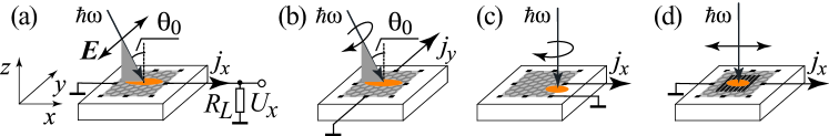
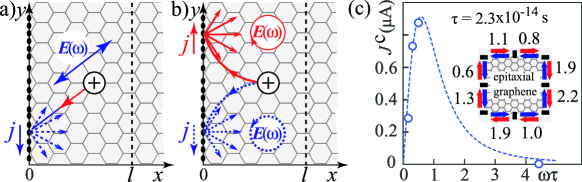
Symmetry analysis permits us to describe the various effects and their observability in terms of macroscopic parameters, such as radiation intensity, polarization and angle of incidence without detailed knowledge of the microsopic origin. Disregarding the substrate, a homogeneous, infinite pristine graphene layer belongs to the centrosymmetric point group. When a substrate or asymmetrically placed adatoms are present, the symmetry is reduced to the the noncentrosymmetric group , removing the equivalence of the and directions. While the photon drag effect can be detected for both kinds of graphene structures photogalvanic effects, which require the lack of inversion symmetry, can not be excited in an infinite homogeneous pristine graphene layer. Symmetry analysis shows that photocurrents in the graphene systems addressed above can be generated for oblique incidence only and may have a contribution along radiation propagation and normal to it, see Fig. 1 (a) and (b). However, in real structures photocurrents excited by perpendicularly incident radiation may become become possible, e.g. when the edges are illuminated, see Fig. 1(c), and symmetry is reduced locally, or in samples with ripples or terraces. The photocurrent at normal incidence may further become possible for graphene with asymmetric metal structures on its top, see Fig. 1 (d), or when an plane static magnetic field is applied. Since second-order phenomena are sensitive to spatial inversion, particular properties of the samples, like the presence of adatoms, terraces, ripples and edges, or the coupling to the substrate become important.
Furthermore, those effects depend strongly on angle of incidence and the radiation polarization. Studying of these dependencies, together with the symmetry analysis, helps to explore microscopic mechanisms responsible for the photocurrent generation. Our works demonstrate that the various possible contributions to the nonlinear response are just proportional to the Stokes parameters, which describe the polarization state of radiation. Hence, when performing measurements of nonlinear high frequency effects in graphene, we vary the radiation polarization state by rotating standard dichroic elements like and plates or Fresnel rhombs with respect to the polarization plane of the linearly polarized laser radiation with (). For light propagating in the direction of the positive axis, the Stokes parameters Saleh ; BornWolf are given by
| (7) |
| (8) |
| (9) |
where defines the radiation intensity, is the azimuth angle defining the orientation of the polarization plane for linearly polarized radiation and and are the angles between the optical axis for half- and quarter wave elements, respectively.
II.2 Experimental
Photocurrents in graphene have been observed and studied applying radiation from near- up to very far-infrared range. To cover a wide frequency range, stretching over three decades from fractions- up to tens of terahertz, various radiation sources have been applied including molecular optically pumped and pulsed lasers at Regensburg Terahertz Center (for laser characteristics see e.g. DMS2009 ; Kvon2008 ; Tunnel1993 ; DX1995 ; spinrelax ; Tunnelingfrequency1998 ), free electron lasers Felbe in Rossendorf detectorFEL1 ; detectorFEL ; FEL1 ; FEL2 and Felix in the Netherlands Knippels99p1578 ; weber2008 , tunable CO2 lasers ganichev_book , quantum cascade lasers Faist1994 ; Faist2000 ; helm2001 and backward wave oscillators Bruenderman2012 . Using of various sources of radiation not only allowed to explore frequency dependencies of the photocurrents under study, but also made possible demonstration of they robustness to high radiation power and examination of the subnanosecond photocurrent dynamics. We emphasize that the photocurrents are detectable at very low power of microWatts and yield response linearly scaling with radiation power up to at least 100 kW without samples damage.
The main experimental geometries used for these studies are outlined in Fig. 1. We illuminated the graphene samples under normal or oblique incidence, with the incidence angle varying from to +40∘. The photocurrents have been measured as a voltage drop across a load resistance, . For experiments with pulsed lasers the photovoltage signal, , was detected by a digital oscilloscope and for radiation modulated with a chopper by using standard lock-in technique. While for the measurements applying pulsed lasers with nanoseconds pulse duration Ohm has been used for radiation in some cases much higher load resistance have been used as well. In the former set-up the photocurrent relates to the photovoltage as , because in all experiments described below the load resistance was much smaller than the sample resistance (). The corresponding photocurrent density is obtained as , where is the width of the graphene sample. The latter configuration greatly increases the magnitude of the voltage signal but complicates the analysis for the case when sample resistance varies substantially with an external parameter, e.g magnetic field or gate voltage. The radiation was focused onto the samples by a parabolic mirror and its power was controlled by photon drag and pyroelectric detectors. The beam shape of the THz radiation is almost Gaussian, measured with a pyroelectric camera Ganichev1999 ; Ziemann2000 .
Photocurrents of different microscopic origins have been observed in a large temperature range from 2 up to 300 K. We emphasize that all observed photocurrents have been also detected at technologically important room temperature. While studying of the temperature dependence also played an important role for understanding the photocurrent formation the largest portion of the research was focused on room temperature response.
II.3 Samples
Terahertz radiation induced photocurrents have been observed and studied in graphene samples prepared applying different technologies including: (i) epitaxial graphene prepared by high temperature Si sublimation of semi-insulating silicon carbide (SiC) substrates Bostwick09 ; Virojanadara08 ; Emtsev2009 ; Seyller2 ; Tzalenchuk2010 ; suppllara2011 ; SwedenPRL2011 , (ii) CVD graphene grown in a conventional chemical vapor deposition process using copper as substrate and catalyst and methane as carbon source Drexler2013 and (iii) exfoliated graphene Bib:Novoselov2004 deposited on oxidized silicon wafers. Details on the growth and characterization of material used for photocurrent studies can be found in karch2010 ; edgePRL2011 ; Drexler2013 ; ratchet_graphene16 ; detectorFEL1 ; detectorFEL ; Emtsev2009 ; Tzalenchuk2010 ; suppllara2011 ; SwedenPRL2011 . The technologies (i) and (ii) allowed us to prepare large area samples with mm2 graphene monolayers while the size of the exfoliated structures was in the range of tens of micrometers. The large size of the epitaxial and CVD samples was of particular importance for the analysis of the photocurrent formation. While both large and small size samples showed the effects, the response of the micron sized exfoliated samples in all type of experiments had an unavoidable contribution of the edge photocurrents discussed in Sec. V. This is because the spot size of the terahertz laser of about 1 mm2 is much larger than the graphene flakes.
Most experiments were carried out on n- and p-type layers with carrier concentrations in the range of ( to )1012 cm-2, Fermi energy of several hundreds of meV, and mobilities about 1000 cm2/Vs at room temperature. We note that in all photocurrent experiments described below were performed in the limit . Thus microscopic theory of the studied phenomena has been developed for the classical regime of light-matter interaction. Thus a microscopic description of each photocurrent under study was obtained by solving the Boltzmann kinetic equation for the electron distribution function . Here is the free-carrier momentum, is the in-plane coordinate and is time.
Electron transport parameters have been obtained from magneto-transport measurements. For some experiments, e.g. on terahertz ratchet effects described in Sec. VII, concentration and type of carriers have been controllably changed applying top and back gate voltages.
To obtain defined graphene edges an edge trim of about 200 m width was removed by reactive ion etching with an argon/oxygen plasma. To protect graphene from uncontrollable change of transport parameters most of samples were encapsulated in a polymer film suppllara2011 , consisting of PMMA/MAA thin film followed by ZEP520 polymer. The unprotected samples were subject to contamination from the ambient atmosphere. The latter has been seen from the change in carrier mobility and density on a time scale of months.
For electrical measurements eight contacts were made in the corners and at the middle of the sides of the square shaped large size graphene layer. The contacts have been fabricated by e-beam deposition of 3 nm Ti and 80 nm Au using a laser-cut shadow mask. Each of the electrodes had 200x200 m2 lateral dimension. Raman spectra taken from several points of each of the samples showed high crystallinity, 1-2 atomic layer thick graphene. Metal contacts to graphene flake has been prepared on the periphery of graphene applying standard lithographic deposition of Ti/Au (3/100 nm) and lift-off.
For studying ratchet effects, metal film superlattices were fabricated on large area epitaxial graphene as well as on small area flakes. A sketch of the superlattices gate fingers and a corresponding optical micrograph are presented in Sec. VII. Preparing gates, first, an insulating aluminium oxide layer was deposited on top of the graphene sheet. The lateral periodic electrostatic potential is created on top of epitaxial graphene by periodic grating-gate fingers fabricated by electron beam lithography and subsequent deposition of metal (5 nm Ti and 60 nm Au). On small area graphene flakes we fabricated inter-digitated metal-grating gates (5 nm/60 nm Ti/Au) TG1 and TG2 having different stripe width and stripe separation. This allowed us to apply different bias voltages to the individual subgrating gates forming the superlattice. The samples were glued onto holders with conductive epoxy utilizing the highly doped silicon wafer as a back gate which enabled us to change type and density of free carriers in graphene. Contact pads were placed in a way that the photo-induced currents can be measured parallel and perpendicular to the metal fingers.
III Photon drag effect
We demonstrated the photon drag effect in graphene produced both by exfoliation and epitaxial techniques karch2010 ; 2010arXiv1002.1047K ; jiangPRB2010 ; GlazovGanichev under oblique incidence of radiation. Electric currents were obtained both in the direction of the radiation propagation (longitudinal geometry) as well as perpendicular to it (transverse geometry). Using the Boltzmann kinetic equation we obtain a microscopic description of the photon drag:
| (10) |
Here, is the velocity, is the kinetic energy, and is the collision integral described in terms of relaxation times () for corresponding angular harmonics of the distribution function 2010arXiv1002.1047K ; GlazovGanichev ; perelpinskii73 . The electric current density is given by the standard equation
| (11) |
where is the electron charge and a factor of 4 accounts for spin and valley degeneracies. We expand the distribution function in powers of electric and magnetic fields, retaining linear and quadratic terms only. Calculations of and are carried out using the energy dispersion of free carriers in graphene and the relation between the velocity and the quasi-momentum (, with being the speed of light). The photon drag current can be generated either due to combined action of the electric and magnetic field of the electromagnetic wave (-mechanism or the dynamic Hall effect) or due to the spatial gradient of the in-plane projection of the radiation electric field (-mechanism). Since in plane waves the complex amplitudes of electric and magnetic fields in Eq. (10) are coupled, (taking and ), both mechanisms share the same origin. Therefore, the dynamic Hall effect can be expressed in terms of the photon drag effect, i.e. . When the effect is treated microscopically in terms of the number of photons (quantum mechanical picture), we speak of the photon drag effect, while the classical picture using the action of electromagnetic fields results in the term dynamic Hall effect.
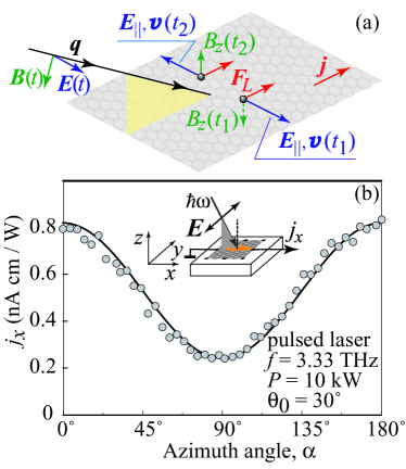
The model of the dynamic Hall effect excited by linearly polarized radiation is illustrated in Fig. 2(a). At one given moment in time, , the Lorentz force caused by the radiation electric and magnetic fields results in a drift in the direction of the light propagation. Half a radiation period later, at time , both fields have changed their sign, therefore, the drift direction remains. Averaging over time, this leads to a time-independent Hall current with fixed direction. The latter depends on the electric field vector orientation and is odd in the angle of incidence, . The additional contribution caused by the -mechanism is also odd in and vanishes for normal incidence. The terms of the fourth-rank tensor which are symmetric and antisymmetric under , yield a photon drag contribution responding to linearly and circularly polarized radiation, respectively (in short: linear and circular photon drag effects) Ivchenko1980 ; belinicher_cpde ; Shalygin2007 ; PhysRevLett.103.103906 . While the longitudinal current can be understood intuitively for arbitrary polarization, the transverse current obtained by circularly polarized radiation is not obvious. It changes its sign upon reversing the helicity of the radiation, and retardation the electric field and the instant velocity of charge carrier has to be taken into account karch2010 . It is most pronounced for . Now, in the schematic model of Fig. 2, the carriers will follow an elliptic orbit instead of a linear trajectory. Due to retardation, the velocity does not immediately track the instantaneous -field direction. Instead, a phase shift equal to between the electric field and the electron velocity ensues. Ultimately, this results in a -component of the Lorentz force , which depends on the direction of electron motion and, consequently, on the radiation helicity. The microscopic theory for the photon drag effect in graphene was developed in Refs. karch2010 ; 2010arXiv1002.1047K for the classical frequency range and in Ref. jiangPRB2010 ; GlazovGanichev for the quantum frequency range.
Experimentally, the photon drag effect, including dynamic Hall effect contribution, was demonstrated both in exfoliated and epitaxial graphene samples for a wide frequency range from fractions of terahertz up to tens of THz karch2010 ; 2010arXiv1002.1047K ; jiangPRB2010 ; GlazovGanichev . We used highly resistive Si or semi-insulating SiC substrates to rule out high losses or shunting by conductive substrates. Due to the mm-size diameter of the Gaussian beam, illumination of the sample edges could not be avoided in the exfoliated samples. This leads to an additional edge current contribution, which is covered in Sec V. Circular and linear photon drag effects have been observed in a wide range of temperatures (from room temperature down to liquid helium temperature) in both n- and p-type layers with carrier concentrations in the range of ( to )1012 cm-2 and mobilities about 1000 cm2/Vs at room temperature, and in a wide range of radiation intensities, from mW/cm2 up to MW/cm2.
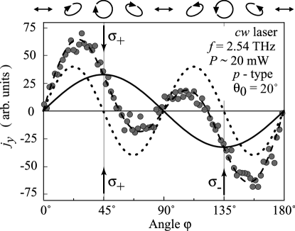
An example of the polarization dependence of the longitudinal photon drag effect is shown in Fig. 2(b). Figure 3 shows transverse photocurrent excited by elliptically polarized radiation in epitaxial single layer graphene. The rotation angle of the quarter-wave plate controls the polarization state of light. The figure reveals thatthe photocurrent is composed of circular and linear terms of comparable strength. Changing from left- to right-handed circular polarization, the circular contribution () changes its sign. In transverse direction, we observe the both the linear and circular contribution, while the signal detected in the incidence plane consists of a linear contribution together with polarization independent current, in agreement with symmetry arguments. The microscopic theory yields
| (12a) | |||
| (12b) |
where and denote linearly independent components of the tensor , and are the axes in the graphene plane, and is the structure normal, the radiation is assumed to be incident in plane, is the unit vector in light propagation direction and is the (complex) polarization vector of radiation, is the circular polarization degree and is the radiation wave vector. The dependence of the photocurrent components on the radiation polarization state, incidence angle and frequency fully agrees with the theory results in karch2010 ; 2010arXiv1002.1047K ; GlazovGanichev . Moreover, only assuming short-range scattering, the microscopic theory yields the absolute value of the photocurrent without fitting parameters karch2010 . Since conduction and valence band are symmetric with respect to the Dirac point, the signal reverses its sign by changing from to -type carriers.
IV Photogalvanics and reststrahl band assisted photocurrents in epitaxial graphene layers
To break inversion symmetry, necessary to observe photogalvanic effects (PGE) 3authors , flat infinite graphene layers can be placed on a substrate or host adatoms on one surface only. This structure inversion asymmetry removes the and equivalence and reduces the symmetry to the point group. The photogalvanic effects give rise to the linear and circular photocurrents 2010arXiv1002.1047K :
| (13a) | |||
| (13b) |
described by two independent parameters and . Unlike in conventional semiconductor quantums well or heterostructures, where the wavefunctions spread over many atomic layer, in graphene carriers are strongly confined to strictly two dimensions and therefore almost do not react to an electric field in -direction. Consequently, the PGE in graphene is reduced when a -component of the radiation field is present. Since both PGE and photon drag show a similar response to polarization, the stronger drag effect usually masks the PGE. To observe the PGE more clearly, the photon drag contribution needs to be reduced, for instance by using high radiation frequencies.
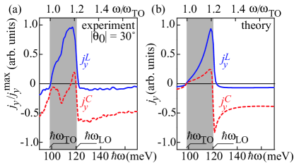
Similar to the orbital mechanisms of the PGE in conventional semiconductor nanostructures, the THz induced PGE here is caused by the quantum interference of the Drude-like indirect optical transitions Tarasenko2007 ; PhysRevB.79.121302 ; tarasenko11 . We observed both linear and circular PGEs in epitaxial graphene samples using mid-infrared radiation of about 30 THz. The observation of PGE is facilitated by the suppression of the photon drag effect at high frequencies and also by the fact that photogalvanic and drag effects lead to opposite signs in their respective contributions to photocurrent. Therefore, by varying the radiation frequency a sign change in the photocurrent was observed, confirming the existence of a PGE with substantial amplitude jiangPRB2010 . The photocurrent due to the circular PGE closely matches the value obtained by a theoretical estimate for a sufficiently strong degree of asymmetry, . We stress that the PGE requires structure inversion asymmetry, which is not present in graphene where the symmetry is preserved, for example, clean, free standing graphene. As will be detailed in Sec. VI, the observation of the magnetic quantum ratchet effect in epitaxial graphene constitutes a nice example of a large structure inversion asymmetry Drexler2013 caused by adatoms or the substrate. Our studies revealed a further interesting feature of photoelectric effects in graphene: A resonance-like frequency dependence for frequencies lying within the reststrahl band of the SiC substrate reststr2013 , see Fig. 4(a). In particular, photocurrents excited by linearly polarized radiation are strongly enhanced just in the range of reststrahlen band, i.e. for frequencies at which the reflection coefficient is close to 100 %. The photocurrent consists of photon drag and PGE contributions of similar strength, responding to the in-plane and out-of-plane components of the local electric field felt by the electrons in the graphene layer. The field distribution at a distance 2 Å from the SiC surface (the position of the graphene layer in our samples, see Ref. Borysiuk ) can be calculated using the macroscopic Fresnel formulas. This model describes the observed resonance surprisingly well. The result of the corresponding photocurrent calculations is shown in Fig. 4(b). Importantly, those observations demonstrate that by engineering the substrate material and spectral range, we can greatly enhance non-linear optical and opto-electronic effects in 2D materials.
V Edge photocurrents
According to the symmetry analysis given in Sec. II.1 illumination of pristine graphene by radiation at normal incidence does not cause an electric current. When the sample edges are illuminated, however, inversion symmetry is broken, and edge photocurrents can be observed. In Fig. 5(a) we illustrate the microscopic process actuating the edge photocurrent. Linearly polarized radiation acts on the free carriers in the semi-infinite graphene plane (). For , the drift motion of the carriers follows the radiation electric field. In one half of the radiation cycle, carriers are moving away from the sample edge. In the other half cycle, they are accelerated towards the sample edge and eventually scattered by edge roughness, randomizing their momentum. On average, they perform a directed motion which is dependent on the angle between linear polarization and the sample edge, resulting in the linear photogalvanic effect. In a narrow stripe close to the sample edge, up to a distance of roughly the mean free path , an electric current is generated. Under circularly polarized radiation, curved trajectories emerge (see Fig. 5(b)), as the carriers try to follow the external electric field. This results in a current reversing its sign, when the radiation helicity changes from (solid) to (dashed). For fixed helicity irradiation of opposite sample edges also results in the opposite sign of the photocurrent.
Boltzmann kinetic equation for describing the edge photocurrents is given by:
| (14) |
where coordinate for a semi-infinite layer, is the carrier charge ( for holes and for electrons), and is the collision integral. The distribution function can be expanded in series of powers of the electric field,
| (15) |
where is the equilibrium distribution function, , and . The oscillating with frequency first order in electric field correction does not contribute to a current. Thus, the current along the structure edge is due to the second order E-field correction and given by
| (16) |
Here factor 4 takes into account the spin and valley degeneracy. The analysis shows that the total current consists of several contributions proportional to four Stokes parameters, which all are observed in experiment.
While the edge photocurrents are detected in both epitaxial and in exfoliated samples, in large-area graphene the analysis of the experiments is substantially easier. In exfoliated graphene, opposite edges of m-sized flakes are illuminated inevitably. In contrast in large-area samples only a single edge can be illuminated. In particular, scanning the laser beam across the sample edges, demonstrated that the coordinate dependence of the signal almost reproduce the the Gaussian beam profile. The red and blue arrows in the inset in Fig. 5(c) illustrate the current directions for and circularly polarized radiation and the numbers show the magnitude of the circular photocurrent for various contact pairs In these measurements the laser spot is always placed between the contacts at which the signal is picked-up, preventing a temperature gradient between contacts. Remarkably, the edge photocurrent proceeds in the same sense of rotation along the edges of the square shaped samples and changes its direction when reversing from to polarization.
Edge photocurrents have been detected in a wide range of radiation frequencies. Figure 5(c) shows the circular edge photocurrent excited by THz radiation as a function of , where is the scattering time at a sample edge. The frequency dependency and magnitudes of the circular edge current agrees well with theory. The only parameter used for fit in Fig. 5(c) is the scattering time close to the edge, which was found to be quite close to the average bulk scattering time. The small differences can most probably be explained by inhomogeneities in the distribution of scatterers Moreover, the sign of the photocurrent excited at fixed helicity reflects the type of the charge carriers close to the edge. The latter has been shown to be holes even for -type epitaxial graphene. This is in accordance with scanning Raman experiments pointing to a -type doping at graphene edges Raman1 ; Raman3 , transport measurements, where a transition from -to -type at the edges of graphene flakes on SiO2 is reported SK_TS4 and growth details of epitaxial graphene Emtsev2009 ; Tzalenchuk2010 ; erl5 . Thus, edge photocurrents may be used to characterize graphene edge properties up to room temperature.
VI Magnetic quantum ratchet effect
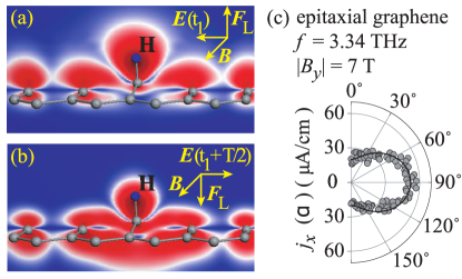
The magnetic quantum ratchet effect has been observed in single-layer graphene samples excited with a pulsed molecular terahertz laser and subjected to an in-plane magnetic field. The physics behind the magnetic quantum ratchet effect is illustrated in Figs. 6(a) and (b). Dirac electrons are driven by the time-dependent electric field and move in alternating directions in the graphene plane. The external static magnetic field leads to a Lorentz force, deflecting the right-moving electrons upwards and the left-moving electrons downwards (see Fig. 6 for an illustration at times and differing by a half a period of the radiation electric field). For spatially symmetric systems this would lead to a zero current. However, when, e.g., top adsorbates are present, spatial symmetry is broken and electrons shifted above or below the graphene plane experience different degrees of disorder, which results in a non-zero current. We note that a similar mechanism was discussed for inversion channels in Si and semiconductor quantum wells Falko89 ; Tarasenko08 ; Tarasenko11 .
The current is proportional to the square of electric field amplitude and the magnetic field strength. Reversing the direction of static magnetic field changes the sign of the photocurrent. It also depends on the angle between the electric field and the static magnetic field . A characteristic polarization dependence of the magnetic ratchet current is shown in Fig. 6(c). The current is maximal for perpendicular electric and magnetic fields and remaining non-zero for parallel fields.The current is well fitted by the equation with two contributions and . Exactly this behaviour follows from the phenomenological and microscopic theory developed in Ref. Drexler2013 and described below.
As an important fact, when comparing two kinds of graphene samples with different surface treatment, we find opposite signs of the slope . While surfaces of samples with graphene encapsulated in a thin polymer film exhibit a positive slope photocurrent, in the sample with unprotected surface the slope is negative, proving differents signs of structure inversion asymmetry (SIA) for both kinds of samples.
We developed a microscopic theory of the observed effect, which agrees beautifully with the experiments and is supported by first-principles calculations. The electric current density is calculated using the general expression Eq. (11)
| (17) |
The distribution function can be obtained from the Boltzmann equation
| (18) |
For elastic scattering, it has the form
| (19) |
where the angular brackets denote impurity ensemble averaging and is the matrix element of electron scattering between the initial and final states with the momenta and , respectively. The ratchet currents originate in the asymmetry of electron scattering, which is caused by the hybridization around the Dirac points in the in-plane magnetic field. Formally, for the magnetic field , it is described by the matrix element
| (20) |
where is the coordinate matrix element between the - and -band states, is the energy distance between the two bands, and are the intraband and interband matrix elements of scattering at zero magnetic field, is the free electron mass, and is the speed of light.
After solving the Boltzmann equation, the analysis of the photocurrent as a function of the radiation polarization reveals that the total current consists of several contributions proportional to four Stokes parameter. Individual contributions proportional to the Stokes parameters describing the degree of linear polarization and the one given by the radiation helicity describes the linear and circular magnetic quantum ratchet photocurrents. Experiments applying radiation with different polarization states demonstrate that all these photocurrents can be excited efficiently in graphene.
VII Terahertz ratchet effects in graphene with a lateral superlattice
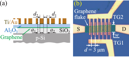
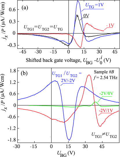
Ratchet effects discussed in the previous section require a static magnetic field. Another efficient way to generate a electric current caused by ratchet effect implies symmetry reduction due to deposition of a periodic asymmetric lateral metal structure on the top of graphene. This type of graphene ratchets has been experimental realized and systematic study in both (i) epitaxially grown and (ii) exfoliated graphene with an asymmetric lateral periodic potential ratchet_graphene16 . The modulated potential has been obtained by fabrication of either a sequence of metal stripes on top of graphene or inter-digitated comb-like dual-grating-gate structures. The latter structure is shown in Figs. 7(a) and (b). Our work demonstrated that a polarization dependent current can be generated by exposing a modulated device to THz laser radiation. By applying different voltages to the two gratings, we can control the photocurrent behaviour at different structure asymmetry, carrier type and density. A typical behaviour of the ratchet photocurrents upon variation of back gate potential is shown in Fig. 8(a) and (b) for various combination of the top dual-grating-gate potentials. Figure 8(a) shows the data for equipotential top gates as a function of the effective back gate which is defined as , where is the applied back gate voltage and are back gate voltages of the charge neutrality point measured for the corresponding top gates voltages. It is seen that the signals are strongly enhanced in the vicinity of the Dirac point and have opposite sign for opposite top gate voltages. A substantial signal is also obtained for zero top gate voltage. This signal is due to the electrostatic potential caused by metal film placed in the proximity of graphene. The data presented in Fig. 8(b) reveal that the photocurrent reflects the degree of asymmetry induced by different top gate potentials and even vanishes for a symmetric profile. The measurements together with a beam scan across the lateral structure prove that the observed photocurrent stems from the ratchet effect.
The experimental data and the theoretical model are discussed by taking the calculated potential profile and near-field effects explicitly into account. The ratchet current consists of the Seebeck thermoratchet effect as well as the “linear” and “circular” ratchets, sensitive to the corresponding polarization of the driving electromagnetic force. The results are analyzed in terms of electronic and plasmonic mechanisms of a photocurrent in periodic structures. The ratchet photocurrent appears due to the noncentrosymmetry of the periodic graphene structure unit cell. The effect of the grating is twofold: (i) it generates a one-dimensional periodic electrostatic potential acting upon the 2D carriers and (ii) it causes a spatial modulation of the THz electric field due to the near field diffraction ratchet_graphene16 ; ratchet2009 ; ratchet2011 ; Review_JETP_Lett ; Theory_PRB_11 . These one-dimensional asymmetries result in the generation of a electric current. The ratchet current may flow perpendicular to the metal fingers or along them. The mechanism leading to the photocurrent formation can be illustrated on the basis of the photocurrent caused by the Seebeck ratchet effect (thermoratchet). This type of ratchet currents can be generated in the direction perpendicular to the metal stripes and corresponds to the polarization independent photocurrent.
The spatially-modulated electric field of the radiation heats the electron gas to footnoteLG . Here is the average electron temperature and oscillates along the -direction with the superlattice period . In turn, the nonequilibrium correction causes an inhomogeneous correction to the conductivity, . Taking into account the spatially modulated electric field we obtain from Ohm’s law the thermoratchet current Theory_PRB_11
| (21) |
Here is the electron charge, and angular brackets denote averaging over a spatial period. This photocurrent vanishes if the temperature is spatially uniform, therefore it is called the Seebeck ratchet current footnoteT1 .
Besides the thermoratchet effect the THz radiation can induce additional photocurrents being sensitive to the linear polarization plane orientation or to the helicity of circularly polarized photoexcitation. These photocurrents have been observed in epitaxially grown graphene with lateral superlattice ratchet_graphene16 . Apart a novel experimental access to the light matter interaction in graphene these results may also have an application potential. Photon helicity driven ratchet current can be utilized for a novel kind of all-electric ellipticity meter. So far such devices implements circular photogalvanic effect in semiconductor quantum wells ellipticitydetector ; ellipticitydetector2 . Unique nonlinear properties of graphene together with the advantages of ratchet photoresponse Review_JETP_Lett ; 16w ; 31 ; 115 ; otsuji2 ; Otsuji_Ganichev can substantially improve detectors detectivity and time resolution as well as extend the operation spectral range.
To summarize this part, experiments on two different types of graphene structures provided a self-consistent picture demonstrating that the photocurrents (i) are generated due to the presence of asymmetric superlattices, (ii) are characterized by specific polarization dependencies for directions along and across the metal stripes, (iii) change direction upon reversing the in-plane asymmetry of the electrostatic potential as well as changing the carrier type, (iv) are characterized by a complex sign-alternating back gate voltage dependence in the vicinity of the Dirac point, (v) are strongly enhanced around the Dirac point and (vi) have potential for development of the all-electric ellipticity meter.
VIII Fast room temperature detectors of THz radiation
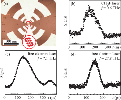
Finally, studying THz radiation induced opto-electronic phenomena in graphene is of particular importance not only for for exploring the physical properties of these materials but also for the development of novel THz radiation detectors. In this section we describe an ultrafast bolometric room temperature graphene based THz detector showing 40 picosecond electrical rise time over a spectral range that spans nearly three orders of magnitude, from the visible to the far-infrareddetectorFEL1 ; detectorFEL . The detector employs a graphene active region with inter-digitated electrodes that are connected to a log-periodic antenna to improve the long-wavelength collection efficiency, see Fig 9(a), and a silicon carbide substrate that is transparent throughout the visible regime. The detector exhibits a noise-equivalent power of approximately 100 W Hz-1/2 and is characterized at frequencies from 0.6 to 384 THz (wavelengths from 500 m to 780 nm). To estimate the noise-equivalent power a calibrated photon-drag detector was used Ganichev84p20 .
Low frequency measurements have been performed with a pulsed THz CH3F laser operating at a frequency of 0.6 THz tunnelreview02 . The laser pulses (about 200 ns duration) are composed of many short peaks (about 1 ns). The repetition rate is 1 Hz and the signals are recorded with a standard digital oscilloscope.
Figure 9(b) shows the graphene detector signal. While the rise time of the detector is less than the pulse duration the detector can be used to analyze the pulse shape. Similar results have been obtained at higher frequencies ranging from 1 to 5 THz by using NH3 as laser active medium.
To explore the time resolution of the graphene detector and extend frequency range to higher frequencies measurements at the free-electron laser FELBE (Dresden-Rossendorf) were performed. The laser provides a pulse train with a repetition rate of 13 MHz at frequencies between 1.3 and 60 THz. Pulse traces for frequencies 7.1 and 27.8 THz are shown in Figs. 9(c) and (d), respectively. The rise time is mainly limited by the parasitic capacitance of the antenna and the inductance of the electrical connections. The intrinsic response time of graphene was determined to be about 10 ps using optical autocorrelation measurements Cai ; detectorFEL1 .
To our knowledge, a similar broad and continuous frequency range of a fast detector was not reported before, and is unique to our device, where graphene as a detector material and SiC substrates are combined. Also, we did not find a significant change in detector response when changing the excitation frequency from inside to just outside the reststrahlen band. The pulse trace shown in Fig. 9(d) is obtained for frequency THz lying within the reststrahlen band.
Our graphene-bases detector enables ultrafast room-temperature detection in a broad frequency range. Given the extremely low heat capacity of charge carriers in graphene, which are heated directly by the incoming radiation, the electron temperature responds strongly. On the other hand, electrons can cool fast and efficiently via optical phonons Hartmann . The presented detector is well suited for a great variety of pulsed laser sources like optical-parametric oscillators and amplifiers or difference-frequency mixers, which makes it a very promising device for multicolor ultrafast spectroscopy.
IX Conclusions and outlook
The physics of nonlinear electron transport and optical phenomena in graphene has already resulted in a great variety of fascinating effects. We still need to develop a full understanding of many of the effects using new experimental and theoretical concepts. For example, tuning the non-linear response using external magnetic fields, strain or by combining graphene with other 2D materials will lead to new insights. Moving beyond graphene, we expect that similar effects can be studied in boron nitride, transition metal dichalcogenieds and topological insulators. For the latter, first experiments have been performed recently HosurBerry ; TopIns4 ; Ultrathin ; TopIns2 ; TopIns5 ; TItheory ; TopIns3 ; Ultrafast ; TopIns1 ; TopIns2add . Finally, from an application point of view, we believe that the described effects will come in useful for material characterization as well as new non-linear devices based on graphene.
Acknowledgements
We are grateful to M.M. Glazov for reading the manuscript and valuable discussions. Financial supported of the DFG (SPP 1459 and GRK 1570) is gratefully acknowledged.
References
- (1) A.H. Castro Neto, F. Guinea, N.M.R. Peres, K.S. Novoselov, A.K. Geim, Rev. Modern Phys. 81, 109 (2009).
- (2) N.M.R. Peres, Rev. Modern Phys. 82, 2673 (2010).
- (3) P. Avouris, Nano Lett. 10, 4285 (2010).
- (4) S. Das Sarma, S. Adam, E.H. Hwang, E. Rossi, Rev. Modern Phys. 83, 407 (2011).
- (5) A. F. Young and P. Kim, Ann. Rev. Cond. Mat. Phys. 2, 101 (2011).
- (6) E. McCann, M. Koshino, Rep. Prog. Phys. 76, 056503 (2013).
- (7) F. Bonaccorso, Z. Sun, T. Hasan, A.C. Ferrari, Nature Photonics 4, 611 (2010).
- (8) T. Mueller, F. Xia, and P. Avouris, Nature Photon. 4, 297 (2010).
- (9) T.J. Echtermeyer, L. Britnell, P.K. Jasnos, A. Lombardo, R.V. Gorbachev, A.N. Grigorenko, A.K. Geim, A.C. Ferrari, and K.S. Novoselov, Nature Commun. 2, 458 (2011).
- (10) M.M. Glazov and S.D. Ganichev, Physics Reports 535, 101 (2014) (2014).
- (11) J. Karch, P. Olbrich, M. Schmalzbauer, C. Zoth, C. Brinsteiner, M. Fehrenbacher, U. Wurstbauer, M. M. Glazov, S. A. Tarasenko, E. L. Ivchenko, D. Weiss, J. Eroms, R. Yakimova, S. Lara-Avila, S. Kubatkin, S. D. Ganichev, Phys. Rev. Lett. 105, 227402 (2010).
- (12) J. Karch, P. Olbrich, M. Schmalzbauer, C. Brinsteiner, U. Wurstbauer, M. M. Glazov, S. A. Tarasenko, E. L. Ivchenko, D. Weiss, J. Eroms, S. D. Ganichev, arXiv cond-mat 1002.1047 (2010).
- (13) C. Jiang, V. A. Shalygin, V. Y. Panevin, S. N. Danilov, M. M. Glazov, R. Yakimova, S. Lara-Avila, S. Kubatkin, S. D. Ganichev, Phys. Rev. B 84, 125429 (2011).
- (14) P. Olbrich, C. Drexler, L. E. Golub, S. N. Danilov, V. A. Shalygin, R. Yakimova, S. Lara-Avila, S. Kubatkin, B. Redlich, R. Huber, and S. D. Ganichev, Phys. Rev. B 88, 245425 (2013).
- (15) J. Karch, C. Drexler, P. Olbrich, M. Fehrenbacher, M. Hirmer, M. M. Glazov, S. A. Tarasenko, E. L. Ivchenko, B. Birkner, J. Eroms, D. Weiss, R. Yakimova, S. Lara-Avila, S. Kubatkin, M. Ostler, T. Seyller, S. D. Ganichev, Phys. Rev. Lett. 107, 276601 (2011).
- (16) D. Sun, C. Divin, J. Rioux, J. E. Sipe, C. Berger, W. A. de Heer, P. N. First, T. B. Norris. Nano Lett. 10, 1293 (2010).
- (17) D. Sun, J. Rioux, J. E. Sipe, Y. Zou, M. T. Mihnev, C. Berger, W. A. de Heer, P. N. First, and T. B. Norris, Phys. Rev. B 85, 165427 (2012).
- (18) D. Sun, C. Divin, M. Mihnev, T. Winzer, E. Malic, A. Knorr, J. E. Sipe, C. Berger, W. A. de Heer, P. N. First, and T. B. Norris, New Journal of Physics 14, 105012 (2012).
- (19) C. Drexler, S. A. Tarasenko, P. Olbrich, J. Karch, M. Hirmer, F. Muller, M. Gmitra, J. Fabian, R. Yakimova, S. Lara-Avila, S. Kubatkin, M. Wang, R. Vajtai, P.M. Ajayan, J. Kono, and S. D. Ganichev, Nature Nanotechnology 8, 104 (2013).
- (20) P. Olbrich, J. Kamann, M. König, J. Munzert, L. Tutsch, J. Eroms, D. Weiss, M.-H. Liu, L. E. Golub, E. L. Ivchenko, V. V. Popov, D. V. Fateev, K. V. Mashinsky, F. Fromm, Th. Seyller, and S. D. Ganichev, Phys. Rev. B 93, 075422 (2016).
- (21) L. Prechtel, L. Song, D. Schuh, P. Ajayan, W. Wegscheider, and A. W. Holleitner, Nature Communications 3, 01 (2012).
- (22) M. W. Graham, S.-F. Shi, D. C. Ralph, J. Park, and P. L. McEuen, Nature Physics 9, 103 (2013).
- (23) M. Mittendorff, S. Winnerl, J. Kamann, J. Eroms, D. Weiss, H. Schneider, and M. Helm, Appl. Phys. Lett. 103, 021113 (2013).
- (24) M. Mittendorff, J. Kamann, J. Eroms, D. Weiss, C. Drexler, S.D. Ganichev, J. Kerbusch, A. Erbe, R.J. Suess, T.E. Murphy, S. Chatterjee, K. Kolata, J. Ohser, J.C. Koenig-Otto, H. Schneider, M. Helm, and S. Winnerl, Optics Express 23, 28728 (2015).
- (25) L. Vicarelli, M. S. Vitiello, D. Coquillat, A. Lombardo, A. C. Ferrari, W. Knap, M. Polini, V. Pellegrini, and A. Tredicucci, Nature Materials 11, 865 (2012).
- (26) M. Freitag, T. Low, F. Xia, and P. Avouris, Nat. Photonics 7, 53 (2013).
- (27) F. H. L. Koppens, T. Mueller, Ph. Avouris, A. C. Ferrari, M. S. Vitiello, and M. Polini, Nature Nanotech. 9, 780-793 (2014).
- (28) R. R. Hartmann, J. Kono, and M. E. Portnoi, Nanotechnology 25, 322001 (2014).
- (29) A. Tredicucci and M.S. Vitiello, IEEE J. Sel. Top. Quant. Electr. 20, 8500109 (2014).
- (30) B. Sturman, V. Fridkin. The photovoltaic and photorefractive effects in non-centrosymmetric materials (Gordon & Breach, Philadelphia, 1992).
- (31) E. L. Ivchenko, G. E. Pikus. Superlattices and other heterostructures (Springer, 1997).
- (32) E. L. Ivchenko. Optical Spectroscopy of Semiconductor Nanostructures (Alpha Science, Harrow UK, 2005).
- (33) S. Ganichev, W. Prettl. Intense Terahertz Excitation of Semiconductors (Oxford University Press, 2006).
- (34) I.D. Yaroshetskii and S.M. Ryvkin, The Photon Drag of Electrons in Semiconductors (in Russian), in Problems of Modern Physics ed. V.M. Tuchkevich and V.Ya. Frenkel (Nauka, Leningrad, 1980), pp. 173-185 [English translation: Semiconductor Physics, ed. V.M. Tuchkevich and V.Ya. Frenkel (Cons. Bureau, New York, 1986), pp. 249-263].
- (35) A.F. Gibson and M.F. Kimmitt, Photon Drag Detection, in Infrared and Millimeter Waves, Vol. 3, Detection of Radiation, ed. K.J. Button (Academic Press, New York, 1980), pp.181-217.
- (36) E.L. Ivchenko and S.D. Ganichev, Spin Photogalvanics in Spin Physics in Semiconductors, ed. M.I. Dyakonov (Springer 2008) pp. 245-277.
- (37) S.D. Ganichev and L.E. Golub, phys. stat. solidi B - basic solid state physics 251, 1801, (2014).
- (38) B. E. A. Saleh, M. C. Teich, Fundamentals of Photonics (John Wiley & Sons, New York, 2003).
- (39) M. Born, E. Wolf, Principles of Optics: Electromagnetic Theory of Propagation, Interference and Diffraction of Light (Cambridge University Press, 1999).
- (40) S. D. Ganichev, S. A. Tarasenko, V. V. Bel’kov, P. Olbrich, W. Eder, D. R. Yakovlev, V. Kolkovsky, W. Zaleszczyk, G. Karczewski, T. Wojtowicz, and D. Weiss, Phys. Rev. Lett. 102, 156602 (2009).
- (41) Z.D. Kvon, S.N. Danilov, N.N. Mikhailov, S.A. Dvoretsky, and S.D.Ganichev, Physica E 40, 1885 (2008).
- (42) S. D. Ganichev, W. Prettl, and P. G. Huggard, Phys. Rev. Lett. 71, 3882 (1993).
- (43) S. D. Ganichev, I. N. Yassievich, W. Prettl, J. Diener, B. K. Meyer and K. W. Benz, Phys. Rev. Lett. 75, 1590 (1995).
- (44) Petra Schneider, J. Kainz, S.D. Ganichev, V.V. Bel’kov, S.N. Danilov, M.M. Glazov, L.E. Golub, U. Rössler, W. Wegscheider, D. Weiss, D. Schuh, and W. Prettl, J. Appl. Phys. 96, 420 (2004).
- (45) S. D. Ganichev, E. Ziemann, Th. Gleim, W. Prettl, I. N. Yassievich, V. I. Perel, I. Wilke, and E. E. Haller, Phys. Rev. Lett. 80, 2409 (1998).
- (46) P. Michel, F. Gabriel, E. Grosse, P. Evtushenko, T. Dekorsy, M. Krenz, M. Helm, U. Lehnert, W. Seidel, R.Wünsch, D.Wohlfarth, A.Wolf, Proceedings of the 2004 FEL Conference, 8-13.
- (47) P. Michel, H. Buettig, F. Gabriel, M. Helm, U. Lehnert, Ch. Schneider, R. Schurig, W. Seidel, D. Stehr, J. Teichert, S. Winnerl, R. Wünsch, The Rossendorf IR-FEL ELBE, Proceedings of the 2006 FEL Conference, 488-491.
- (48) G. M. H. Knippels, X. Yan, A. M. MacLeod, W. A. Gillespie, M. Yasumoto, D. Oepts, and A. F. G. van der Meer, Phys. Rev. Lett. 83, 1578 (1999).
- (49) W. Weber, L.E. Golub, S.N. Danilov, J. Karch, C. Reitmaier, B. Wittmann, V.V. Bel’kov, E.L. Ivchenko, Z.D. Kvon, N.Q. Vinh A.F.G. van der Meer, B. Murdin, and S.D. Ganichev, Phys. Rev. B 77, 245304 (2008).
- (50) J. Faist, F. Capasso, D. L. Sivco, C. Sirtori, A. L. Hutchinson, A. Y. Cho, Science 264, 553 (1994).
- (51) J. Faist, F. Capasso, C. Sirtory, D.L. Sivko, and A.Y. Cho, Quantum Cascade Lasers, in series Semiconductors and Semimetals, eds.R.K. Willardson and E.R. Weber, Vol. 66, Intersubband Transitions in Quantum Wells, Volume eds. H.C. Liu and F. Capasso (Academic Press, San Diego, 2000)
- (52) M. Helm, Infrared long wavelength infrared emitters based on quantum wells and superlattices (Gordon & Breach Science Publishers, Amsterdam, 2000).
- (53) E. Bruendermann, H.-W. Huebers, and M.F. Kimmitt, Terahertz Techniques in Springer Series in Optical Sciences, (Springer-Verlag, Berlin and Heidelberg, 2012)
- (54) S. D. Ganichev Physica B 273-274, 737 (1999).
- (55) E. Ziemann, S. D. Ganichev, I. N. Yassievich, V. I. Perel, and W. Prettl, J. Appl. Phys. 87, 3843 (2000).
- (56) A. Bostwick, T. Ohta, T. Seyller, K. Horn, and E. Rotenberg, Nature Phys. 3, 36 (2007).
- (57) C. Virojanadara, M. Syväjarvi, R. Yakimova, L. I. Johansson, A. A. Zakharov, and T. Balasubramanian, Phys. Rev. B 78, 245403 (2008).
- (58) K. V. Emtsev, A. Bostwick, K. Horn, J. Jobst, G. L. Kellogg, L. Ley, J. L. McChesney, T. Ohta, S. A. Reshanov, J. Rohrl, E. Rotenberg, A. K. Schmid, D. Waldmann, H. B. Weber, and T. Seyller, Nature Materials 8, 203 (2009).
- (59) M. Ostler, F. Speck, M. Gick, T. Seyller, Phys. Stat. Sol. B 247, 2924 (2010).
- (60) A. Tzalenchuk, S. Lara-Avila, A. Kalaboukhov, S. Paolillo, M. Syvajarvi, R. Yakimova, O. Kazakova, J. J. B. M., V. Fal’ko, and S. Kubatkin, Nature Nanotechnology 5, 186 (2010).
- (61) S. Lara-Avila, K. Moth-Poulsen, R. Yakimova, T. Bjornholm, V. Fal’ko, A. Tzalenchuk, S. Kubatkin, Advanced Materials 23, 878 (2011).
- (62) S. Lara-Avila, A. Tzalenchuk, S. Kubatkin, R. Yakimova, T. J. B. M. Janssen, K. Cedergren, T. Bergsten, and V. Fal’ko, Phys. Rev. Lett. 107, 166602 (2011).
- (63) K. S. Novoselov, A. K. Geim, S. V. Morozov, D. Jiang, Y. Zhang, S. V. Dubonos, I. V. Grigorieva, and A. A. Firsov, Science 306, 666 (2004).
- (64) V. I. Perel’ and Ya. M. Pinskii, Sov. Phys. Solid State, 15, 688 (1973).
- (65) E. L. Ivchenko, G. E. Pikus, in Semiconductor Physics (Cons. Bureau, New York, 1986).
- (66) V. I. Belinicher, Sov. Phys. Solid State 23, 2012 (1981).
- (67) V. Shalygin, H. Diehl, C. Hoffmann, S. Danilov, T. Herrle, S. Tarasenko, D. Schuh, C. Gerl, W. Wegscheider, W. Prettl, S. Ganichev, JETP Letters 84, 570 (2007).
- (68) T. Hatano, T. Ishihara, S. G. Tikhodeev, N. A. Gippius, Phys. Rev. Lett. 103, 103906 (2009).
- (69) S.D. Ganichev, E. L. Ivchenko, and W. Prettl, Physica E 14, 166 (2002).
- (70) S. Tarasenko, JETP Letters 85, 182 (2007).
- (71) P. Olbrich, S. A. Tarasenko, C. Reitmaier, J. Karch, D. Plohmann, Z. D. Kvon, S. D. Ganichev, Phys. Rev. B 79, 121302 (2009).
- (72) S. A. Tarasenko, Phys. Rev. B 83, 035313 (2011).
- (73) J. Borysiuk, R. Bozek, W. Strupinski, A. Wysmolek, K. Grodecki, R. Stepniewski, and J. M. Baranowski, J. Appl. Phys. 105, 023503 (2009).
- (74) C. Casiraghi, A. Hartschuh, H. Qian, S. Piscanec, C. Georgi, A. Fasoli, K. S. Novoselov, D. M. Basko, and A. C. Ferrari, Nano Lett. 9, 1433 (2009).
- (75) S. Heydrich, M. Hirmer, C. Preis, T. Korn, J. Eroms, D. Weiss, and C. Schüller, Appl. Phys. Lett. 97, 043113 (2010).
- (76) E. J. H Lee, K. Balasubramanian, R. Thomas Weitz, M. Burghard, and K. Kern, Nature Nano. 3, 486 (2008).
- (77) F. Speck, J. Jobst, F. Fromm, M. Ostler, D. Waldmann, M. Hundhausen, H. B. Weber, Th. Seyller, Appl. Phys. Lett. 99, 122106 (2011).
- (78) V. I. Falko, Fiz. Tvedr. Tela 31, 29 (1989) [Sov. Phys. Solid State 31, 561 (1989)].
- (79) S. A. Tarasenko, Phys. Rev. B 77, 085328 (2008).
- (80) S. A. Tarasenko, Phys. Rev. B 83, 035313 (2011).
- (81) P. Olbrich, E. L. Ivchenko, T. Feil, R. Ravash, S. D. Danilov, J. Allerdings, D. Weiss, and S. D. Ganichev, Phys. Rev. Lett. 103, 090603 (2009).
- (82) P. Olbrich, J. Karch, E. L. Ivchenko, J. Kamann, B. März, M. Fehrenbacher, D. Weiss, and S. D. Ganichev, Phys. Rev. B 83, 165320 (2011).
- (83) E. L. Ivchenko and S. D. Ganichev, JETP Lett. 93, 673 (2011).
- (84) A. V. Nalitov, L. E. Golub, and E. L. Ivchenko, Phys. Rev. B 86, 115301 (2012).
- (85) Here we assume the Boltzmann statistics for clarity. The case of the Fermi-Dirac statistics and real situation of degenerate carriers are studied in ratchet_graphene16 ; Theory_PRB_11 .
- (86) Hereafter we consider a graphene sheet with the lateral potential . The electron energy in each valley, or , is given by , and the two-dimensional wave vector is referred to the vortex of the hexagonal Brillouin zone. Since in the model under consideration the behavior of electrons in the or valleys is identical we consider the current generation in one of them and then double the result.
- (87) S.N. Danilov, B. Wittmann, P. Olbrich, W. Eder, W. Prettl, L.E. Golub, E.V.Beregulin, Z.D. Kvon, N.N. Mikhailov, S.A. Dvoretsky, V.A. Shalygin, N.Q. Vinh, A. F.G. van der Meer, B. Murdin, and S.D. Ganichev, J. Appl. Phys. 105, 013106 (2009).
- (88) S. Dvoretsky, N. Mikhailov, Y. Sidorov, V. Shvets, S. Danilov, B. Wittman, and S. Ganichev, J. Electron. Mat. 39, 918 (2010).
- (89) V. V. Popov, J. Infr. Millim. THz Waves 32, 1178 (2011).
- (90) V. V. Popov, D. V. Fateev, T. Otsuji, Y. M. Meziani, D. Coquillat, and W. Knap, Appl. Phys. Lett. 99, 243504 (2011).
- (91) E. S. Kannan, I. Bisotto, J.-C. Portal, T. J. Beck, and L. Jalabert, Appl. Phys. Lett. 101, 143504 (2012).
- (92) S.A. Boubanga-Tombet, Y. Tanimoto, A. Satou, T. Suemitsu, Y. Wang, H. Minamide, H. Ito, D. V. Fateev, V.V. Popov, and T. Otsuji, Appl. Phys. Lett. 104, 262104 (2014).
- (93) P. Faltermeier, P. Olbrich, W. Probst, L. Schell, T. Watanabe, S. A. Boubanga-Tombet, T. Otsuji, and S. D. Ganichev, J. Appl. Phys. 118, 084301 (2015).
- (94) S. D. Ganichev, Y. V. Terent’ev, and I. D. Yaroshetskii, Pisma Zh. Tekh. Fiz. 11, 46 (1985) [Sov. Tech. Phys. Lett. 11, 20 (1989)].
- (95) S.D. Ganichev, I.N. Yassievich, and W. Prettl, J. Phys.: Condens. Matter 14, R1263 (2002).
- (96) X. Cai, A. B. Sushkov, R. J. Suess, M. M. Jadidi, G. S. Jenkins, L. O. Nyakiti, R. L. Myers-Ward, S. Li, J. Yan, D. K. Gaskill, T. E. Murphy, H. D. Drew and M. S. Fuhrer, Nat. Nanotechnol. 9, 814 (2014).
- (97) P. Hosur, Phys. Rev. B 83, 035309 (2011).
- (98) J.W. McIver, D. Hsieh, H. Steinberg, P. Jarillo-Herrero, N. Gedik, Nat. Nanotechnol. 7, 96 (2012).
- (99) Quan Sheng Wu, Sheng Nan Zhang, Zhong Fang, Xi Dai, Physica E 44, 895 (2012)
- (100) P. Olbrich, L.E. Golub, T. Herrmann, S.N. Danilov, H. Plank, V.V. Bel’kov, G. Mussler, Ch. Weyrich, C.M. Schneider, J. Kampmeier, D. Grützmacher, L. Plucinski, M. Eschbach, S.D. Ganichev, Phys. Rev. Lett. 113, 096601 (2014).
- (101) Junxi Duan, Ning Tang, Xin He, Yuan Yan, Shan Zhang, Xudong Qin, Xinqiang Wang, Xuelin Yang, Fujun Xu, Yonghai Chen, Weikun Ge, Bo Shen, Sci. Rep. 4, 4889 (2014).
- (102) V. Kaladzhyan, P.P. Aseev, S.N. Artemenko, Phys. Rev. B 92, 155424 (2015).
- (103) K.-M. Dantscher, D.A. Kozlov, P. Olbrich, C. Zoth, P. Faltermeier, M. Lindner, G.V. Budkin, S. A. Tarasenko, V.V. Bel’kov, Z. D. Kvon, N.N. Mikhailov, S.A. Dvoretsky, D. Weiss, B. Jenichen, S.D. Ganichev, Phys. Rev. B 92, 165314 (2015)
- (104) Christoph Kastl, Christoph Karnetzky, Helmut Karl, A.W. Holleitner, Nat. Commun. 6, 6617 (2015).
- (105) K.N. Okada, N. Ogawa, R. Yoshimi, A. Tsukazaki, K.S. Takahashi, M. Kawasaki, Y. Tokura, Phys. Rev. B 93, 081403 (2016).
- (106) H. Plank, L.E. Golub, S. Bauer, V.V. Bel’kov, T. Herrmann, P. Olbrich, M. Eschbach, L. Plucinski, C.M. Schneider, J. Kampmeier, M. Lanius, G. Mussler, D. Grützmacher, S.D. Ganichev, Phys. Rev. B 93, 125434 (2016).