Neutron irradiation test of Hamamatsu, SensL and AdvanSiD UV-extended SiPMs
Abstract
In this paper, we report the measurement of the neutron radiation hardness of custom Silicon Photomultipliers arrays (SiPMs) manufactured by three companies: Hamamatsu (Japan), AdvanSiD (Italy) and SensL (Ireland). These custom SiPMs consist of a array of mm2 monolithic cells with pixel sizes of respectively m (Hamamatsu and SensL) and m (AdvanSid).
A sample from each vendor has been exposed to neutrons generated by the Elbe Positron Source facility (Dresden), up to a total fluence of n1MeV/cm2. Test results show that the dark current increases almost linearly with the neutron fluence.
The room temperature annealing was quantified by measuring the dark current two months after the irradiation test. The dependence of the dark current on the device temperature and on the applied bias have been also evaluated.
1 Introduction
Silicon Photomultipliers (SiPMs) are semiconductor photon-counting devices composed by a matrix of Avalanches Photo Diodes (APDs) operating in Geiger mode. Their working point is few volts above the breakdown voltage and their output signal is the sum of the charge produced by each APD pixel fired by a photon. The active area and the shape of a SiPM, as well as the dimension of the pixels, can often be customised according to the user’s needs [2].
To be used in High Energy Physics, SiPMs have to withstand many years of operation in harsh radiation environments where both ionising and non-ionising dose are delivered. On reference [3], we have tested Hamamatsu [4] SiPMs up to 200 Gy using a 60Co source, observing negligible effects on gain and leakage current. In this paper, we have investigated the damage induced by neutrons on SiPMs manufactured by three companies: Hamamatsu (Japan), AdvanSid (Italy) [5] and SensL (Ireland) [6]. The SiPMs under test were custom-arrays, each one constituted by a array of mm2 monolithic cells with pixels size of 50 m for Hamamatsu and SensL, and 30 m for AdvanSid. The tested SiPMs were designed with a thermal package having a thermal resistance below , in order to improve their dissipation capabilities with respect to the standard models and allow better cooling.
Three samples, one per vendor, have been exposed to the same neutron fluence at the Elbe Positron Source (EPOS) facility of the Helmholtz-Zentrum Dresden-Rossendorf (HZDR), Dresden in March 2017 [7].
The main effects of radiation on Silicon are: (i) the bulk damage, caused by the displacement of crystal atoms, and (ii) the surface damage, which includes all effects in the covering dielectrics and in the interface region [8][9]. Both types of damage cause an increase of leakage current and noise, change in material resistivity, reduction in the amount of collected charge due to the charge carrier trapping mechanism and decrease of the carrier’s mobility and their lifetime. In out test, both type of damage have not been distinguished.
2 The EPOS - HZDR Facility
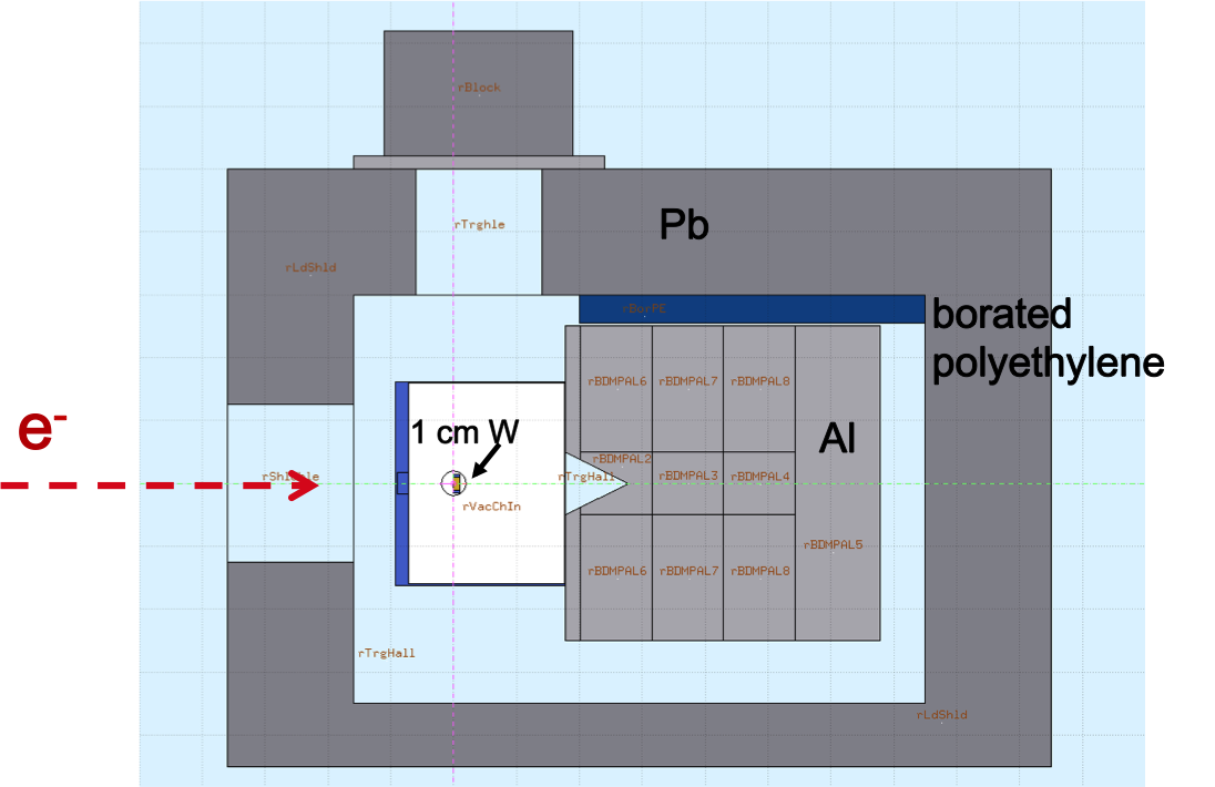
In the EPOS facility, a 30 MeV electron beam, of O(100 A) current, interacts with 1 cm thick Tungsten target and becomes a source of photon and neutrons [10]. In Figure 1, the picture of the target with the surrounding shielding of Lead and Borated Polyethylene is shown.
 |
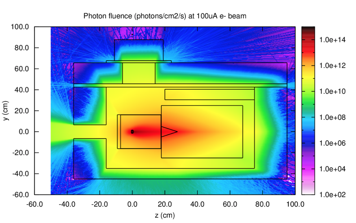 |
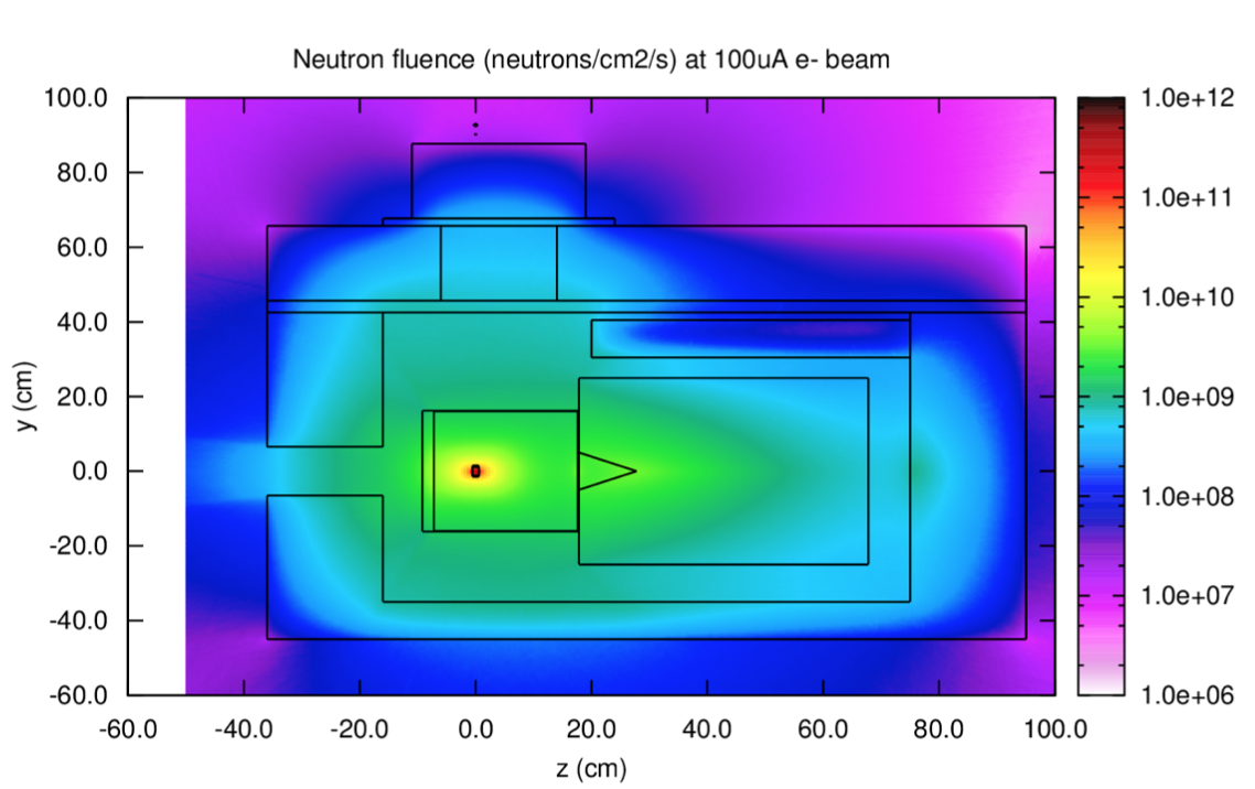
In Figure 2 the distribution of the equivalent expected dose for neutrons is shown on left, while on right the distribution of the expected dose due to photons is presented. The devices under test were located on top of the shielding roof, where the expected photons contribution in dose is negligible. The ratio between the expected photon and neutron induced doses in this region is of .
 |
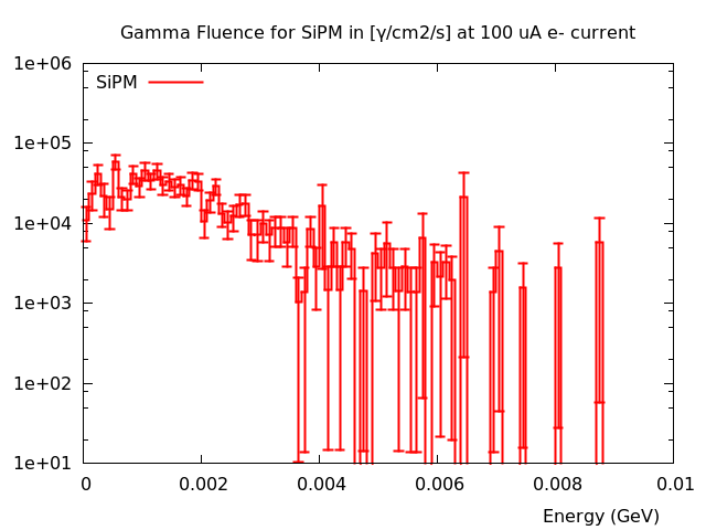 |
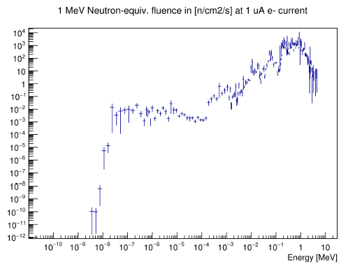
During the irradiation period, that lasted 29 hours, we have continuously recorded the beam current in order to monitor the flux intensity along the data taking time. The neutron fluence has been estimated by a full FLUKA simulation [11] and has been scaled to a 1 MeV equivalent neutron damage on Silicon as a function of the kinetic energy of the simulated neutrons. The spectrum (Figure 3, left) is well centred around 1 MeV. Most of the photon produced have an energy below 3 MeV, as shown in Figure 3 (right), so they are well shielded by lead.
3 Experimental setup and measurements
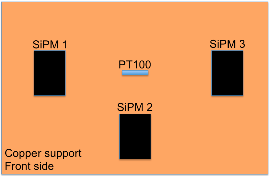
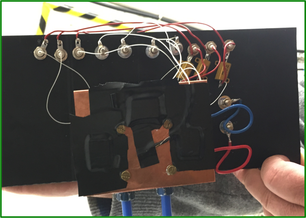
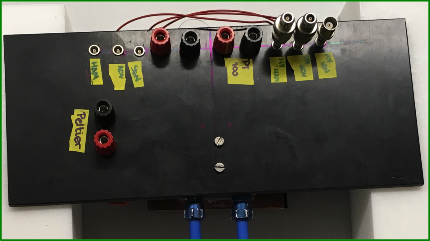
The three samples, one per vendor, have been exposed simultaneously to the same neutron flux. The sketch of the experimental setup is shown in Figure 4, where the details of the SiPM support are shown.
 |
 |
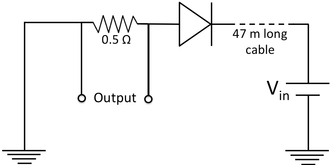
The sketch of the used readout circuit is shown in Figure 5. To evaluate the dark current, the acquired output voltage has been divided by the value (0.5 ) of the load resistor.
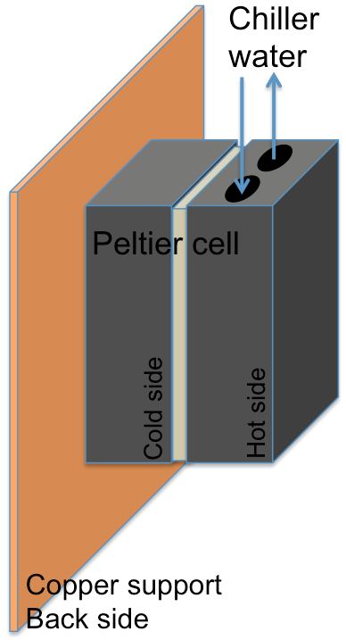
To maintain the SiPMs’ temperature as stable as possible, the sensors under test have been plugged on a copper support, which has been mounted on the cold side of a Peltier cell. In order to assure a good thermal contact, a thermal paste has been used to couple the sensor to the copper plate. The Peltier cell hot side was connected to a very stable chiller system, with water coolant, running at (18.3 0.1 ) ∘C. This allowed us to maintain the other side at around 20∘ C. To monitor the SiPMs temperature along the run, a PT100 resistance thermometer have been plugged in the middle of the SiPMs in the copper support. This resistance temperature detector is made by a ceramic material with an accurate resistance-temperature relationship.
The SiPM output voltages and the PT100 temperature were acquired by an Agilent 34972A LXI Data Acquisition / Data Logger Switch Unit every 10 s [12]. Pictures of the experimental setup are shown in Figure 6.
 |
 |
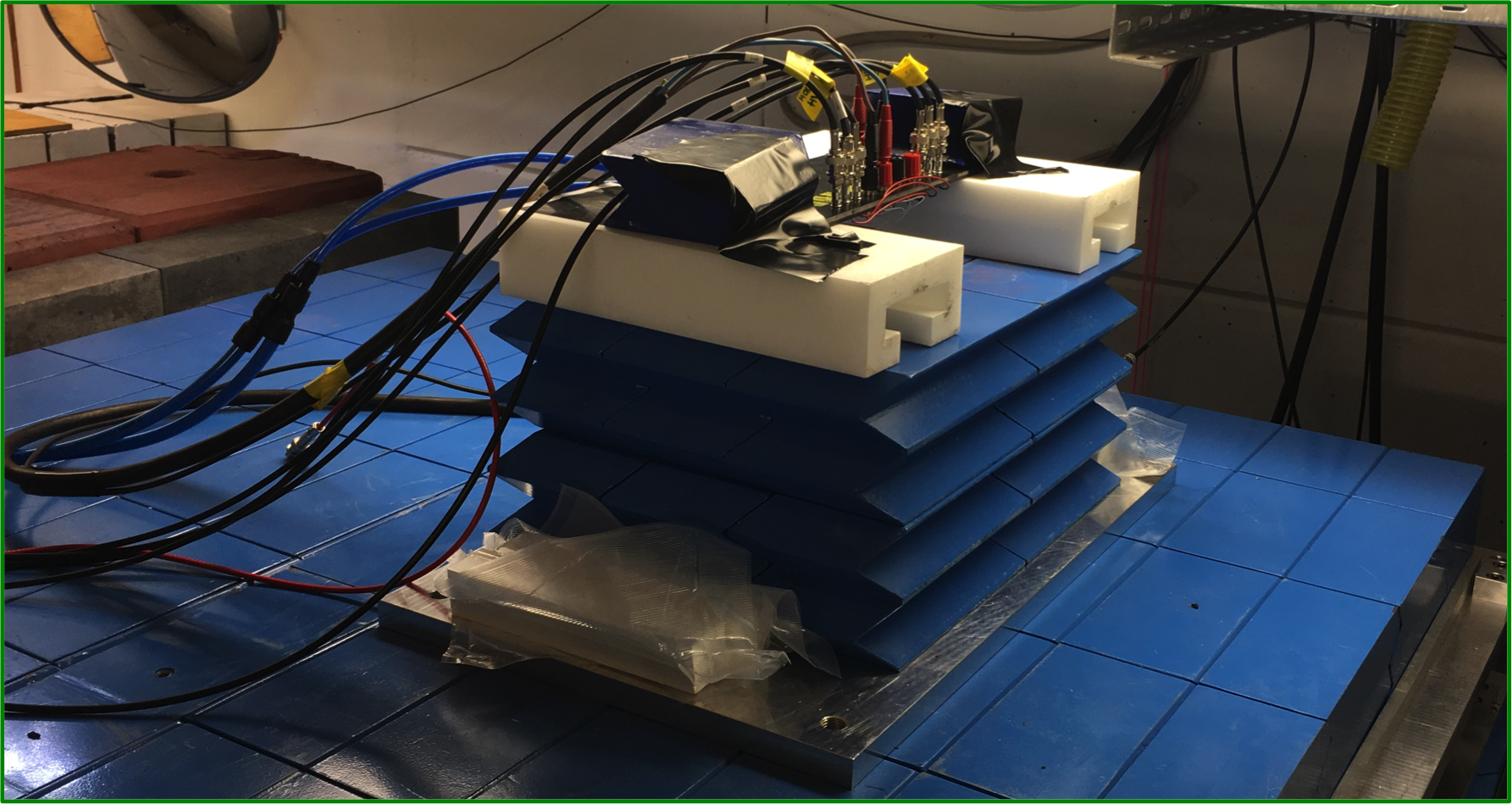
The SiPM support has been placed on the top of the shielding at 90 cm far away from the neutron source, with the sensors active area positioned perpendicular to the incoming neutrons, as shown in Figure 7. For each SiPM, only one out of six cells has been biased at the operating voltage, while the other five cells were not biased. During the irradiation, we have continuously measured the current drawn by the biased cells.
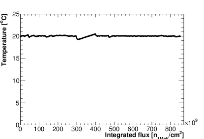
As shown in Figure 9 (left), the Peltier cell and the chiller system were performing well and were able to maintain the copper temperature stable around 20 ∘C.
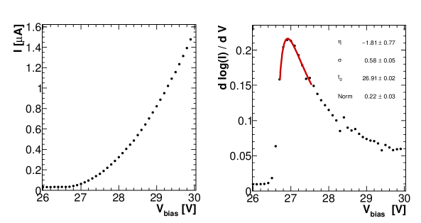
The operational voltage (Vop), of each cell of the SiPMs under test, has been determined in our laboratory in Frascati and has been set at 3 V over the breakdown voltage (). The has been evaluated with the method of maximization of the current Logarithmic Derivative (LD), that is d(log I)/dV [13]. To perform this measurement, the SiPMs have been inserted inside a darkened black box. The dark current as a function of the bias voltage has been recorded using a Keithley pico-ammeter. An example of the current LD as a function of the bias voltage is shown in Figure 8.
The total neutron fluence absorbed by the SiPMs at the end of the 29 hours long test was estimated to be n/cm2.
In Figure 9 (right), the measured current of the biased cells as a function of the integrated flux are reported for the three tested SiPMs. To summarise the measurements performed at EPOS, the temperature, Vop and the dark current (Id) at the end of the irradiation are reported in Table 1 for each SiPM.
 |
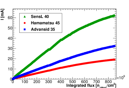 |
| SiPM | T | Vop | Id | Id |
|---|---|---|---|---|
| vendor | (after months) | |||
| [∘C] | [V] | [mA] | [mA] | |
| AdvanSiD 35 | 20 | 29.9 | 32.4 | 19.1 |
| Hamamatsu 45 | 20 | 54.7 | 19.5 | 10.0 |
| SenSL 40 | 20 | 27.9 | 62 | 38.8 |
The current dependance on neutron fluence is well represented by a linear behaviour up to about 15 mA.
At the end of the irradiation period, we have also measured the currents of the unbiased cells that resulted to be few % larger than the biased ones. The dark current increase of the Hamamatsu SiPM looks much smaller than the Advansid and Sensl ones.
4 Current measurement after months of annealing
We have continued to measure the current for about 22 hours after the end of the beam exposure, as shown in Figure 10.
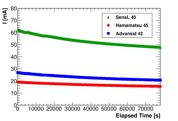
A current decrease due to room temperature annealing is clearly visible. Indeed, two months after the end of the irradiation test, a leakage current reduction of about 50% has been observed as shown in Table 1 (last column). The SiPM cells biased during irradiation have been tested to determine the dark current variation with respect to a change in temperature and bias voltage. The experimental setup previously described has been inserted in a light-tight, insulated box, fluxed with nitrogen, in order to decrease the temperature without reaching the dew point.
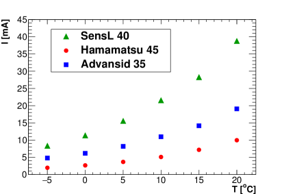
The dark current (Id) has been measured by first varying the temperature of the SiPMs and then varying the operational voltage at fixed temperature.
The SiPMs temperature has been decreased from 20 ∘C down to -5C. In order to keep unchanged the operational point while varying the temperature, the bias voltage has been decreased by per degree, as from technical specifications. This voltage adjustment has been cross-checked by measuring, for each SiPM, the breakdown voltage at 20, 10 and 0 ∘C.
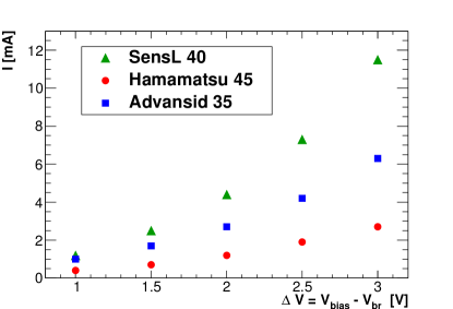
The variation of the measured Id with respect to temperature is reported in Figure 11 (left). A decrease of 10 ∘C in the SiPM temperature corresponds to a decrease of about 50% in Id. After completing this first study, the SiPM temperature has been fixed at 0 ∘C and the current has been acquired at different bias voltages. Results are reported in Figure 11 (right), as a function of the difference between the bias and the breakdown voltage (). Also in this case, a reduction of the working points quickly diminishes the drawn dark current.
 |
 |
5 Conclusions
The neutron radiation damage for three custom SiPMs from different vendors (AdvanSiD, Hamamatsu and SensL) have been determined using neutrons generated at the EPOS facility of HZDR, Dresden. The SiPMs used consisted of the parallel configuration of two series of three mm2 cells. The dark current of the SiPMs increases linearly as a function of the 1 MeV equivalent neutron fluence up to 15 mA, while a deviation from linearity is observed at larger dark currents, as due to the additional voltage drop in the 47 m long cable.
The dark current increase in the SensL and AdvanSiD sensors resulted to be much faster than that of Hamamatsu SiPMs. At the end of the irradiation period, the dark current values were of 62 mA, 32.4 mA and 19.5 mA for SensL, AdvanSiD and Hamamatsu respectively. After two months of annealing at room temperature the dark current values decreased by a factor of two.
We have also been observing that lowering the sensor temperature of 10 ∘C, as well as decreasing the bias voltage of 1 V/cell, corresponds to a reduction of an additional factor of two in the dark current.
Acknowledgments
This work was supported by the EU Horizon 2020 Research and Innovation Program under the Marie Sklodowska-Curie Grant Agreement No.690385. The authors are grateful to many people for the successful realisation of the tests. In particular, we thank all HZDR-EPOS staff, for providing a necessary and well equipped facility, and all the LNF technicians helping for making this test a reality.
References
- [1]
- [2] G. Bondarenko et al., Multi-pixel Photon Detectors,NIM A242 (2000).
- [3] S. Baccaro et al., Radiation hardness test of un-doped CsI crystals and Silicon Photomultipliers for the Mu2e calorimeter, submitted to JPCS (2016) [arXiv:1606.07255].
-
[4]
http://www.hamamatsu.com/us/en/index.html -
[5]
https://srs.fbk.eu/optimization-sipm-technology -
[6]
http://sensl.com/ -
[7]
https://www.hzdr.de - [8] G. Lindstrom et al., Radiation Damage in Silicon Detectors, NIM A512 (2003) [arXiv:0211118].
- [9] A. Konobeyev et al., Neutron displacement cross-sections for structural materials below 800 MeV, JNuM 186 (1992) [DOI: 10.1016/0022- 3115(92)90328- I].
-
[10]
https://www.hzdr.de/db/Cms?pOid=12516&pNid=3453 -
[11]
http://www.fluka.org/fluka.php -
[12]
https://www.testequity.com/documents/pdf/34970A-34972A-QFS.pdf - [13] F. Nagy et al., A model based DC analysis of SiPM breakdown voltages, NIM A849 (2017) [DOI: 10.1016/j.nima.2017.01.002, arXiv:1606.07805]