[figure]style=plain,subcapbesideposition=top \shortdate\settimeformatampmtime
acmcopyright \isbn978-1-4503-4927-7/17/06\acmPrice$15.00 http://dx.doi.org/10.1145/3061639.3062293
On Mitigation of Side-Channel Attacks in 3D ICs: Decorrelating Thermal Patterns from Power and Activity
Abstract
Various side-channel attacks (SCAs) on ICs have been successfully demonstrated and also mitigated to some degree. In the context of 3D ICs, however, prior art has mainly focused on efficient implementations of classical SCA countermeasures. That is, SCAs tailored for up-and-coming 3D ICs have been overlooked so far. In this paper, we conduct such a novel study and focus on one of the most accessible and critical side channels: thermal leakage of activity and power patterns. We address the thermal leakage in 3D ICs early on during floorplanning, along with tailored extensions for power and thermal management. Our key idea is to carefully exploit the specifics of material and structural properties in 3D ICs, thereby decorrelating the thermal behaviour from underlying power and activity patterns. Most importantly, we discuss powerful SCAs and demonstrate how our open-source tool helps to mitigate them.
<ccs2012> <concept> <concept_id>10002978.10003001.10010777.10011702</concept_id> <concept_desc>Security and privacy Side-channel analysis and countermeasures</concept_desc> <concept_significance>500</concept_significance> </concept> <concept> <concept_id>10010583.10010600.10010601</concept_id> <concept_desc>Hardware 3D integrated circuits</concept_desc> <concept_significance>500</concept_significance> </concept> <concept> <concept_id>10010583.10010662.10010586</concept_id> <concept_desc>Hardware Thermal issues</concept_desc> <concept_significance>300</concept_significance> </concept> <concept> <concept_id>10010583.10010662.10010674.10011722</concept_id> <concept_desc>Hardware Chip-level power issues</concept_desc> <concept_significance>300</concept_significance> </concept> <concept> <concept_id>10010583.10010682.10010697.10010700</concept_id> <concept_desc>Hardware Partitioning and floorplanning</concept_desc> <concept_significance>300</concept_significance> </concept> </ccs2012>
[500]Security and privacy Side-channel analysis and countermeasures \ccsdesc[500]Hardware 3D integrated circuits \ccsdesc[300]Hardware Thermal issues \ccsdesc[300]Hardware Chip-level power issues \ccsdesc[300]Hardware Partitioning and floorplanning
1 Introduction
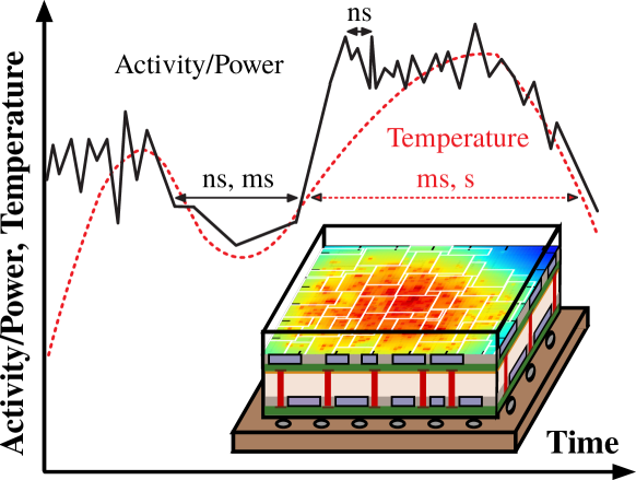
Side channels represent the physical interactions any electronic device triggers in its surrounding, e.g., electromagnetic radiation or heat dissipation. Side-channel attacks (SCAs) then seek to retrieve sensitive information (e.g., secret keys) by carefully monitoring those physical interactions [1, 2, 3]. For example, Skorobogatov and Woods [3] extracted an embedded AES key from a military-grade FPGA using an advanced attack on the power side channel. Another practical and effective side channel is the thermal leakage of power and activity patterns [4, 5]. Being the scope of our work, this side channel is elaborated in detail in Section 2.
3D integration is expected to successfully meet the increasingly demanding requirements for modern ICs, such as high performance, increased functionality, and low power consumption [6, 7, 8]. While previous studies, early prototypes, and first commercial products have focused on memory-logic integration (e.g., see [7, 8, 9]), there is recent progress towards logic stacking as well, also driven by technology innovations such as direct wafer bonding [6].
One major concern for 3D integration in general and for 3D logic ICs in particular is the thermal and power management, which is furthermore highly technology dependent [10, 11, 12]. In practice, 3D ICs will require runtime capabilities for thermal management, based on embedded on-chip thermal sensors [9, 13, 14].
SCAs in the context of 3D ICs have only recently come into focus, and studies such as [15] mainly discuss how structural properties of 3D ICs may help in mitigating SCAs. The full potential of SCAs specifically tailored for and targeting on 3D ICs has not been explored yet. It is intuitive that SCAs developed for 2D ICs may not be successful in 3D ICs, due to the different physical structures of 2D and 3D ICs. Still, a practical SCA could be based on thermal readings of 3D ICs, which is realistic due to the availability of and relatively easy access to on-chip thermal sensors [5, 9, 13, 14].
SCA countermeasures in 3D ICs such as [16, 17] leverage 3D integration mainly for efficient implementation of prior techniques. For example, to mitigate timing-based SCAs on caches, Bao and Srivastava [16] exploit the reduced latencies in 3D ICs in order to implement random eviction and latency scattering, which are otherwise (in the context of 2D ICs) arguably too costly measures.
The work of Gu et al. [18] seeks to mitigate thermal-related leakage in 3D ICs, and is of particular interest here. The authors propose to integrate (along with the actual functional circuitry) thermal sensors, thermal-noise generators as well as runtime controllers. These primitives “inject dummy activities” when-/wherever considered necessary and, hence, aim for smooth thermal profiles to hinder thermal profiling of module activities. However, there are major shortcomings of this work. First, the concept appears not specifically tailored for 3D ICs—it does not explicitly address the different structural and material properties, different heat paths or thermal coupling effects in 3D ICs, nor does it elaborate on the implementation of 3D ICs. Second, the “injection” principle causes further power dissipation, which may be prohibitive for thermal- and power-constrained 3D ICs in the first place. This shortcoming is confirmed by an observation in [18] itself: the best leakage-mitigation rates are only achievable for the highest injection rates.
In this work, we take a fundamentally different approach by considering security as a design parameter. We propose an SCA-aware floorplanning methodology that decorrelates the thermal behaviour from power and activity patterns, protecting against a very practical and potentially effective threat for the security of 3D ICs.
2 Background and Scope
2.1 Thermal Side Channel
The thermal side channel (TSC) has recently gained more attention, also thanks to case studies such as [4, 5]. For example, Masti et al. [5] have shown for Intel Xeon multi-core processors that () process executions on one core can be detected in adjacent cores, and that () different processes, when scheduled by turns in one core, can build a covert channel with up to 12.5 bit/s.
The TSC is particularly attractive for three reasons: () it is easy to access via widely available on-chip sensors [5, 9, 13, 14]; () it provides internal and external leakage of activity/computation patterns through thermal variations [4, 5]; and () it may serve as proxy for the power side-channel using temperature-to-power interpolation techniques such as [19]. An attacker can obtain localized thermal readings either directly or estimate them, e.g., using interpolation techniques. We note that interpolation techniques have been demonstrated to achieve high-accuracy and high-resolution estimates of both power and temperatures in large-scale 3D ICs [9].
In general, an attacker can monitor the thermal patterns of an IC either at regular runtime or when he/she applies specific input patterns, crafted to reveal the activity of sensitive components. We address both scenarios for the attacker’s capabilities and the SCAs we formulate (Section 5) and evaluate (Section 7).
Practical limitations of the TSC are the following:
-
•
The classical heat equation models power and temperature as linearly correlated. In practice, however, this behaviour is constrained by material properties, i.e., thermal conductivities and capacitances both within and across the boundaries of chips [4]. In other words, a linear correlation of (secret) activity patterns and (leaked) thermal patterns is only applicable for homogeneous material properties. This has direct implications for our work, as elaborated in Section 3.
-
•
Due to relatively large thermal capacitances and resistances present in modern ICs, especially in 3D ICs, the internal heat flow is much slower than the underlying activity/power patterns (Figure 1). That is, the TSC has a relatively low bandwidth, which hinders the leakage of highly dynamic computation [4]. We assume strong capabilities for practical attacks (Section 5), rendering the TSC attractive nevertheless.
-
•
As with any side channel, the TSC experiences noisy readings; the heating effects of active modules are both spatially and temporally superposed. For any 2D/3D IC, these noise patterns may range from negligible to dominant effects, depending on the floorplan, the resulting power distribution, the material properties, and the heat paths along with their dissipation capabilities. Our assumptions for the attacker’s capabilities address and mitigate also this limitation (Section 5).
2.2 Scope of Our Work
In this novel work, we focus on the design-time mitigation of thermal-related SCAs in 3D ICs. In contrast, previous work leverages 3D ICs only as implementation option for available (2D) SCA countermeasures, or neglects key aspects of 3D ICs (Section 1).
Our key idea is the following: we exploit the specifics of material and structural properties in 3D ICs, in order to effectively decorrelate thermal patterns from the power and activity patterns.
We conduct our study in the context of 3D floorplanning for two reasons. First, optimizing the thermal and power distributions of 3D ICs is essential (due to their high integration densities), and floorplanning is widely acknowledged as an appropriate design stage to do so [20, 10, 11]. Second, chip designer typically have to reuse some “black box” intellectual-property (IP) modules, with limited access to only basic properties (e.g., area, inputs/outputs, power), while they still hope to mitigate potential SCAs. Our methodology is applicable in such scenarios through leakage-aware design techniques during block-level floorplanning.
We make our work publicly available within the open-source 3D floorplanner Corblivar [21]; see Sections 6 and 7 for details.
3 Initial Findings
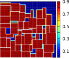
We next discuss exploratory experiments for through-silicon via (TSV)-based 3D ICs with two dies.111Thermal maps would be considerably different for other 3D integration flavors, e.g., for monolithic 3D ICs [12]. Our leakage-mitigation techniques are generic; they may be tailored towards different flavors, which will be the scope for future work. For the thermal analysis we use HotSpot 6.0 [22]. We model the heatsink atop the 3D IC, the signal TSVs acting as “heat-pipes” between stacked dies, and also the secondary path conducting heat towards the package. Further details are given in Section 7. We investigated all 30 combinations of 5 different power distributions (globally uniform, locally uniform, medium gradients, small gradients, and large gradients) and 6 different TSV distributions (no TSVs; maximal TSV density, i.e., 100% of area covered by TSVs and their keep-out zones; irregular TSVs; irregular TSVs along with regular TSVs; irregular groups of densely packed TSVs, i.e., TSV islands; and TSV islands along with regular TSVs). Note that some of these power and TSV distributions are impractical, yet relevant for exploratory experiments. Figure 2 illustrates a few selected power and thermal maps.
The key initial finding for thermal-leakage trends in 3D ICs is that the correlation of activity/power patterns and the thermal behaviour mainly depends on both () the power-density distributions and () the TSV distributions. We observe high correlations for:
-
()
non-uniform power distributions with large gradients, both within dies and across dies. For example, Figure 2(e–h) exhibits large power gradients, while Figures 2(a–d) and 2(i–l) show somewhat smooth gradients. We observe the lowest correlations for globally uniform power distributions (Figure 2[a–d]), which are, however, artificial and impractical. Locally uniform power distributions are more realistic, and we observe that such distributions exhibit low correlations as well, especially along with irregular TSVs or distributed TSV islands. For example, comparing Figure 2(k, l) with Figure 2(c, d), we observe largely decorrelated thermal patterns, although the underlying power distribution of the former appears notably more diverse than its counterpart.
-
()
large numbers of regularly arranged TSVs. For example, see Figure 2(e–h) with regularly placed TSVs and TSV islands versus Figures 2(a–d) with irregularly placed TSVs and 2(i–l) with only TSV islands. Note that the use of few regular TSVs and/or TSV islands may locally further reduce the correlation. For example, see Figure 2(j), where a local thermal minima is observable in the lower right region, despite the relatively high power density underlying (Figure 2[i]).
It may be more intuitive to formulate these findings vice versa—the less regular and/or fewer the TSVs, the lower is the correlation. As indicated for the limitations of the TSC (Subsection 2.1), an unbiased and high correlation is only found in homogeneous structures. Inserting copper/tungsten-based TSVs into the silicon dies invalidates that assumption, especially when TSVs are few and irregularly distributed.
4 Models for Thermal Leakage
4.1 Correlation and Correlation Stability
We propose the Pearson correlation of power and thermal maps as a key metric for thermal-related leakage. Note that the Pearson correlation is also the underlying measure for the side-channel vulnerability factor (SVF) [23], an established metric for the vulnerability of ICs in terms of information leakage via side channels.
Along with our assumptions for the attacker’s capabilities (Section 5), the Pearson correlation is comparably meaningful as the SVF. That is, the lower the correlation, the lower the leakage of power/activity patterns via the TSC, and the lower the vulnerability of the IC. Given the power and thermal maps of a 3D IC, we measure the correlation coefficient on each die separately:
| (1) |
where are the average power and temperature values, respectively, and are the individual values, both over all locations in die . The locations/values are to be organized in grids with same dimensions for both power and thermal maps/grids.
Note that Equation 1 models the correlation only for one steady-state case, i.e., for arbitrary but fixed power and temperature values. We propose another correlation measure to capture the runtime stability of correlation for locations/bins on die :
| (2) |
with different sets of activities, where power and temperature readings may vary notably. The lower the stability , the lower the thermal leakage for various ranges of power/activity patterns at particular locations within the die of the 3D IC.
[] \sidesubfloat[]
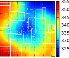 \sidesubfloat[]
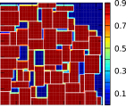 \sidesubfloat[]
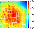
\sidesubfloat[]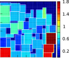 \sidesubfloat[]
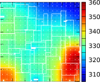 \sidesubfloat[]
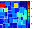 \sidesubfloat[]
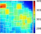
\sidesubfloat[] \sidesubfloat[]
 \sidesubfloat[]
 \sidesubfloat[]
4.2 Spatial Entropy of Power Maps
As proposed by Claramunt [24], the spatial entropy assesses the dispersion of the classical entropy over some regions. It is based on two principles: () the closer the different entities, the higher the spatial entropy; and () the closer the similar entities, the lower the spatial entropy. We note that this is in good correspondence to the phenomenon of heat distribution—the closer the differently powered heat sources, the higher the spatial entropy of the superposed thermal responses, i.e., the thermal gradients; and the closer the similarly powered heat sources, the lower the thermal gradients.
Hence, our notion for modeling the spatial entropy of power maps is to anticipate the degree of the thermal gradients; recall that large thermal gradients hint on large thermal leakage (Section 3). Our formulation, derived from [24], measures the spatial entropy of power maps in 3D ICs for each die as follows:
| (3) |
where are classes of similar-value power ranges, and and are the average spatial inter- and intra-class distances. We calculate those distances according to [24], in which we use Manhattan distances for bins (i.e., class members) in the equidistant power-map grids we construct for each die. For fast and effective classification of those grids, we employ nested-means partitioning: the power values are first sorted, then recursively bi-partitioned with the current mean defining the cut, and the partitioning proceeds until the standard deviation within any class approaches zero.
As the spatial entropy does not account for thermal analysis and subsequent correlation calculations, it lacks the capability to verify the actual leakage. It is, however, suitable for fast estimation of the potential leakage during floorplanning loops/iterations. During our experiments (Sections 3 and 7), we observe the following trend for the bottom die (), even for different TSV patterns: the lower the spatial entropy, the lower the power-temperature correlation.
5 Thermal Side-Channel Attacks
Our assumptions: An attacker has direct and physical access to the targeted 3D IC, but can conduct only non-invasive attacks.222In contrast to 2D ICs, we may expect invasive probing and reverse engineering of 3D ICs to be notably more difficult and costly. That is, he/she may apply (arbitrary) input patterns and observe both the actual outputs and the thermal behaviour of the 3D IC.We also assume that the attacker has a system-level understanding of the 3D IC, e.g., as obtained from datasheets. This is important for purposefully crafting input patterns to trigger certain activities.
We make further strong assumptions enabling an attacker to circumvent the critical limitations of the TSC (Subsection 2.1). First, the attacker can stabilize the 3D IC’s activity with the help of specifically crafted, repetitive input patterns. Second, he/she may await the thermal steady-state response after applying any input. Both assumptions ensure that the TSC readout correlates only with the input patterns. Third, the attacker has unlimited access to all thermal sensors, spread across the 3D IC, and can thus obtain high-accuracy and continuous thermal readings of any (part of a) module at will.
We believe that these assumptions are relevant and practical when attacking security-critical (3D) ICs. For example, a security module may check whether a provided password is correct, and only then trigger data decryption. The thermal patterns for complex decryption operations will be relatively easy to distinguish from simple matching operations for password checks. An attacker may then brute-force a password even when the security module itself is “silent”, i.e., when it would not directly react to wrong passwords.
Attacks based on the TSC in 3D ICs are formulated next, with consideration of the attacker’s capabilities outlined above. Note that similar attacks have been discussed and successfully conducted on classical (2D) microcontrollers by Hutter and Schmidt [4].
-
1.
Thermal characterization of the 3D IC: This is typically an exploratory attack, and others may follow as outlined below. Step by step, the attacker will apply a broad and varied range of input patterns in order to trigger as many activity patterns as possible. By monitoring the TSC, he/she can then build a model for the thermal behaviour of the 3D IC.
-
2.
Localization and monitoring of modules: The attacker targets on particular modules by applying crafted input patterns; the objective is to trigger these modules and observe thermal variations exclusively or at least predominantly within these modules. Given the attacker’s lack of implementation details and hence the lack of a precise input-to-activity mapping, this attack is typically applied iteratively, with varying inputs. In case the characterization attack outlined above has been successfully applied, those efforts may be much lower. Once the thermal response is confined to particular regions, i.e., modules of interest are localized with some confidence, further attacks may be applied. Most notably, an attacker may now observe the sensitive activity/computation of particular modules by monitoring them during runtime.
6 Methodology
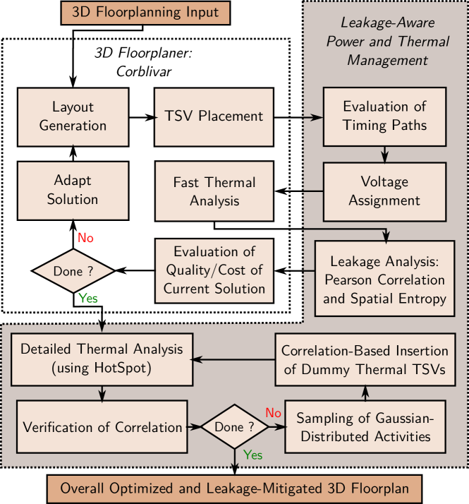
The objective of our work is to account for thermal leakage in 3D ICs directly and continuously within the floorplanning stage that also optimizes for classical criteria. That is, during our iterative floorplanning flow (Figure 3), we memorize the 3D floorplans with lowest correlations coefficients and spatial entropies (Section 4) as best in terms of thermal leakage, but we select the final solution while also accounting for other criteria such as wirelength and critical delays; see Section 7 for details of our setups.
We implement and publicly release all our techniques within Corblivar [25, 21]. We opt for this 3D floorplanning framework mainly because it is multi-objective, modular, and competitive. An for our work essential feature of Corblivar is its fast thermal analysis, which enables us to continuously estimate the correlation. However, we found this fast analysis to be inferior to the detailed analysis of HotSpot [22], especially for diverse arrangements of TSVs. Thus, we also verify the final correlation after floorplanning.
6.1 Management of Power Distributions
Recall that non-uniform power distributions with large gradients induce notable thermal leakage (Section 3). A key measure in our work is thus the management of global and local power distributions. To this end, we develop efficient algorithms for floorplanning-centric voltage assignment, a technique well-known for power management in 2D ICs [26], but so far mostly overlooked for 3D ICs.
For any floorplan layout, we initially estimate the timing paths. We do so because the prospects for voltage assignment depend primarily on timing slacks—the more slack a module has, the lower the voltage we may apply, and the more controllable its power and thermal footprints become. We estimate the net delays via the well-known Elmore delays (here with consideration of wires and TSVs), and the delays of modules are estimated as proposed in [27].
Voltage volumes—the generalized 3D version of voltage domains spanning across multiple dies—are constructed next. We do so by considering each module individually as the root for a multi-branch tree representation of voltage volumes. Each tree/volume is recursively build up via a breadth-first search across the respectively adjacent modules. During this merging procedure, we update the resulting set of feasible voltages, i.e., the voltages we may commonly apply for all modules within the volume without violating any timing/delay constraints. As result, a finalized tree represents a set of practical voltage volumes: each node comprises a volume, and all the modules and voltages are encoded in the node and its ancestors.
Finally, we select voltage volumes such that we optimize () for locally uniform power densities within volumes, and () for small power gradients across volumes, as motivated by our initial findings (Section 3). To this end, we target for lowest standard deviations of power values both within voltage volumes and across volumes.
We found that our techniques induce a low runtime cost, around 30%, when compared to 3D floorplanning without voltage assignment. This is noteworthy because previous work [27, 28] employ computationally-expensive MILP formulations which render their integration into 3D floorplanning flows impractical in the first place.
6.2 Sampling of Activities and Post-processing
To impersonate an attacker triggering various activity patterns by alternating the inputs at runtime, we model the power profiles of all modules as Gaussian distributions. Without loss of generality, we set up each distribution with the module’s nominal power value as mean and a standard deviation of 10%. We stepwise evaluate all the steady-state temperatures using HotSpot [22] and sample the correlation stability (Equation 2) in 100 runs over the whole 3D IC.
Continuing the runtime sampling process, we iteratively insert dummy thermal TSVs where the most stable correlations occur, as long as the resulting average correlation is reduced. This stop criterion represents the final “sweet spot” where further TSV insertion would increase the overall correlation again (Subsection 7.1).
7 Experimental Evaluation
We select arbitrary GSRC and IBM-HB+ benchmarks, and their properties are reviewed in Table 1. Note that we scale up the modules’ footprints in order to obtain sufficiently large dies; 3D ICs are only superior to 2D ICs for large-scale integration [10, 25, 20]. The resulting die outlines are fixed, making the floorplanning problem practical yet challenging [25]. For stacking of the two dies, we assume the face-to-back fashion [20, 6] (see also Figure 1). Further technical details such as material properties and TSV dimensions are given in the respective default configurations of [22, 21].
Each benchmark is floorplanned 50 times in two different setups: () power-aware floorplannning and () TSC-aware floorplanning. It is important to note that setup () provides a competitive and challenging baseline for the evaluation of (). Unlike we do in (), most previous work did not account for continuous optimization of the voltage assignment within the optimization loops, and may have thus missed on the full potential of power-aware 3D floorplanning.
For (), we optimize the packing density, wirelength, critical delay, peak temperature, and voltage assignment, all at the same time; all criteria are weighted equally. For voltage assignment we seek to minimize both the overall power and the number of required voltage volumes. For (), we consider the same criteria as for (), rendering it a practical and competitive setup. Additionally, we seek to minimize both the average correlation coefficients and the average spatial entropies. Here, for voltage assignment, we now seek to minimize () the number of required voltage volumes and () the standard deviations of power gradients among and across different volumes. For implementing the voltage volumes in both setups () and (), we consider three options: 0.8V, with power scaling of 0.817 and delay scaling of 1.56; 1.0V, without impact on power/delay; and 1.2V, with 1.496 power scaling and 0.83 delay scaling. These values are simulated for the 90nm node [27].
| Name | # Modules | Modules’ | # Nets | # Terminal | Outline | Power (for |
| (Hard/Soft) | Scale Factor | Pins | [] | 1.0V) [W] | ||
| n100 | (0/100) | 10 | 885 | 334 | 16 | 7.83 |
| n200 | (0/200) | 10 | 1,585 | 564 | 16 | 7.84 |
| n300 | (0/300) | 10 | 1,893 | 569 | 23.04 | 13.05 |
| ibm01 | (246/665) | 2 | 5,829 | 246 | 25 | 4.02 |
| ibm03 | (290/999) | 2 | 10,279 | 283 | 64 | 19.78 |
| ibm07 | (291/829) | 2 | 15,047 | 287 | 64 | 9.92 |
7.1 On Destabilizing the Leakage Correlation
A low runtime stability of correlations is crucial to thwart TSC attacks (Section 5): the lower the correlation for various inputs, the less likely an attacker succeeds when modeling the thermal leakage. We observe that our techniques greatly reduce both the runtime stability of correlations and the nominal, steady-state correlations.
Consider Figure 4 as an example. In order to meet timing constraints, some modules (colored red in Figure 4[a]) had to have high voltages assigned. The accordingly high power consumption of those modules disrupts the otherwise more uniform power distribution (Figure 4[b]). As a result, for varying activity patterns triggered by an attacker, the highest stability of correlations occurs around those modules. Our post-processing stage consequently inserts dummy TSVs there (see black dots in Figure 4[a]). For the nominal case, i.e., for average activity patterns, the resulting shift in thermal behaviour is reflected in Figure 4(c, d). In this example, the correlation coefficient drops from 0.461 to 0.324. This means that an attacker seeking to retrieve sensitive activities based on thermal readings is on average 30% less likely to succeed.
We find that the insertion of dummy thermal TSVs may stabilize the correlation again, by inducing adverse side-effects on previously more decorrelated regions. For example, consider the upper left corner in Figure 4(c, d): the local correlation there increased to some degree, due to the insertion of TSVs in the other, previously highly correlated regions like the lower right corner. To account for such trade-off effects, recall that our post-processing stage inserts dummy TSVs only as long as the overall correlation decreases. Alternatively, we may adapt that stage to focus on reducing the correlation stability primarily for the critical module(s) to be protected from TSC attacks, and to accept more stable correlations elsewhere.
[] \sidesubfloat[]
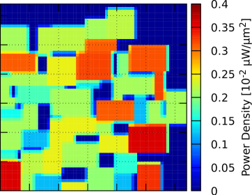
\sidesubfloat[] \sidesubfloat[]
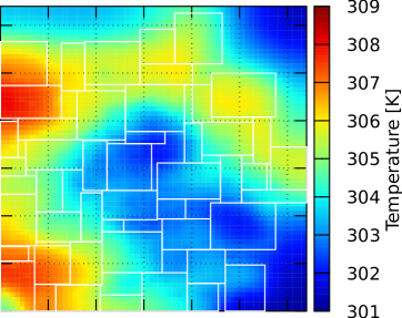
7.2 Leakage Trends and Mitigation Rates
To understand general trends on the thermal leakage in 3D ICs and the mitigation rates offered by our techniques, we next discuss the average ranges of spatial entropies and correlation coefficients over 50 runs (Figure 5 and Table 2). However, it is important to note that these numbers do not reflect well on best cases, which a designer will select carefully depending on the needs for security and the margin for design cost; see Subsection 7.3 for the latter.

When comparing the power-aware and the TSC-aware results, the key observation is that the latter exhibit lower correlations for the bottom die (), by 16.79% for the largest GSRC benchmark n300, by 15.25% for the largest IBM-HB+ benchmark ibm03, and by 7.71% over all benchmarks on average. While the average reduction over all benchmarks may appear somewhat low, its impact is important. It translates directly to 7.71% higher noise on average for an attacker, and to an accordingly higher degree of freedom for a designer to employ sensitive modules. Besides, a noteworthy trend here is the scalability: the larger the circuit, the lower the correlation achieved by our TSC-aware floorplanning.
Both the power-aware and the TSC-aware setup can achieve low correlations for the bottom die, but at the cost of notably higher correlations for the top die. This limitation is due to the following: since the heatsink is attached above the top die, Corblivar [25, 21] by default employs a thermal design rule to place high-power modules preferably into the top die. In turn, this results in large power gradients across the two dies as well as within the top die. Large gradients in the top die naturally increase its correlation. Furthermore, the large disparities between the two dies obfuscate any “heat injection” from the bottom die into the top die which may otherwise decrease the top die’s correlation, e.g., see Figure 2(e–h) versus Figure 2(a–d). While we may relax Corblivar’s design rule, we found that this prohibitively increases the peak temperatures.
7.3 Design Impact and Effectiveness
Next, we discuss the average impact on other design criteria (Table 2). Again, these results are relevant to understand general trends, while they do not represent particular corner cases.
Recall that a key measure in our methodology is the management of global and local power distributions, realized by tailored voltage assignment. Our technique increases power only by 5.38% on average when compared to power-aware floorplanning, whose key criterion is minimal power. Despite this (limited) increase of power, we observe notable reductions of the steady-state peak temperatures, namely by 13.22% on average (i.e., with respect to the ambient temperature of 293K). We consider this as a beneficial side-effect of our multi-objective and iterative 3D floorplanning flow.
Besides, we observe an average impact on other criteria as follows: wires are 1.08% longer, critical delays increase by 10.33%, and, most notably, 87.17% more voltage volumes are implemented.
Finally, we note that () power- and TSC-aware floorplanning exhibit the same average number of signal TSVs, and that () TSC-aware floorplanning employs only few additional thermal TSVs (1.37% on average). Both findings indicate that our TSC-aware floorplanning realizes the reported low correlation not only by carefully inserting dummy TSVs, but more so by thoroughly exploring the 3D design space. This is achieved for the first time thanks to our effective and efficient floorplanning techniques.
| Power-Aware Floorplanning | Thermal Side-Channel-Aware Floorplanning | |||||||||||||
| Metric | GSRC Benchmarks | IBM-HB+ Benchmarks | GSRC Benchmarks | IBM-HB+ Benchmarks | ||||||||||
| n100 | n200 | n300 | ibm01 | ibm03 | ibm07 | Avg | n100 | n200 | n300 | ibm01 | ibm03 | ibm07 | Avg | |
| Spatial Entropy | 2.787 | 3.718 | 4.315 | 4.462 | 3.830 | 3.727 | 3.806 | 2.735 | 3.635 | 4.350 | 4.348 | 4.040 | 3.689 | 3.799 |
| Correlation Coefficient | 0.476 | 0.249 | 0.274 | 0.199 | 0.459 | 0.446 | 0.351 | 0.471 | 0.238 | 0.228 | 0.189 | 0.389 | 0.426 | 0.324 |
| Spatial Entropy | 2.982 | 3.905 | 4.237 | 2.752 | 1.061 | 3.314 | 3.041 | 2.868 | 3.698 | 4.086 | 2.668 | 1.140 | 3.219 | 2.946 |
| Correlation Coefficient | 0.708 | 0.642 | 0.625 | 0.771 | 0.928 | 0.694 | 0.728 | 0.719 | 0.662 | 0.649 | 0.795 | 0.919 | 0.695 | 0.739 |
| Overall Power [W] | 7.890 | 7.801 | 12.522 | 4.291 | 27.038 | 10.737 | 11.713 | 10.331 | 8.172 | 12.967 | 4.520 | 26.829 | 11.247 | 12.344 |
| Critical Delay | 0.833 | 0.784 | 1.164 | 1.49 | 3.54 | 2.82 | 1.771 | 0.878 | 0.817 | 1.162 | 1.607 | 3.831 | 3.434 | 1.954 |
| Wirelength | 30.671 | 29.086 | 37.100 | 21.491 | 57.999 | 108.020 | 47.394 | 32.956 | 28.733 | 33.928 | 21.913 | 57.449 | 112.468 | 47.907 |
| Peak Temp [22] | 309.811 | 308.475 | 311.095 | 303.496 | 334.759 | 308.715 | 312.725 | 315.563 | 309.246 | 312.168 | 303.459 | 311.066 | 309.201 | 310.117 |
| Signal TSVs | 451 | 897 | 1,100 | 3,489 | 3,809 | 10,740 | 3,414 | 451 | 897 | 1,099 | 3,490 | 3,806 | 10,741 | 3,414 |
| Dummy Thermal TSVs | – | – | – | – | – | – | – | 64 | 29 | 25 | 3 | 16 | 144 | 47 |
| Voltage Volumes | 6.900 | 12.365 | 14.365 | 3.675 | 5.333 | 3.027 | 7.610 | 9.705 | 17.048 | 19.658 | 14.256 | 12.909 | 11.888 | 14.244 |
| Runtime [s] | 83 | 218 | 262 | 489 | 197 | 507 | 226 | 287 | 531 | 524 | 1075 | 374 | 667 | 576 |
8 Conclusion
In this work, we address the thermal leakage of secret computation/activity patterns within up-and-coming 3D ICs. In general, thermal side-channel attacks are considered practical and effective; this is in contrast to other laborious attacks such as invasive probing, which are for 3D ICs presumably even more difficult.
We model thermal leakage as a built-in criteria into floorplanning and minimize it using novel and efficient techniques, thereby incorporating security early on in the 3D IC design flow. Our techniques are based on the key findings that thermal leakage in 3D ICs depends on and, thus, can be controlled by the power distributions along with the arrangement of through-silicon vias.
For future work, we shall address the thermal leakage in larger 3D-IC stacks and for other flavours such as monolithic integration.
References
- [1] M. Rostami et al., “A primer on hardware security: Models, methods, and metrics,” Proc. IEEE, vol. 102, no. 8, pp. 1283–1295, 2014.
- [2] Y. Zhou and D. Feng, “Side-channel attacks: Ten years after its publication and the impacts on cryptographic module security testing,” in IACR Crypt. ePrint Arch., no. 388, 2005.
- [3] S. Skorobogatov and C. Woods, “In the blink of an eye: There goes your AES key,” in IACR Crypt. ePrint Arch., no. 296, 2012.
- [4] M. Hutter and J.-M. Schmidt, “The temperature side channel and heating fault attacks,” in Smart Card Research and Advanced Applications, ser. Lect. Notes Comp. Sci. Springer, 2014, vol. 8419, pp. 219–235.
- [5] R. J. Masti et al., “Thermal covert channels on multi-core platforms,” in Proc. USENIX Sec. Symp., 2015, pp. 865–880.
- [6] (2016) International technology roadmap for semiconductor 2.0. ITRS. [Online]: http://www.semiconductors.org/main/2015_international_technology_roadmap_for_semiconductors_itrs/
- [7] D. H. Kim et al., “3D-MAPS: 3D massively parallel processor with stacked memory,” in Proc. Int. Sol.-St. Circ. Conf., 2012, pp. 188–190.
- [8] S. S. Iyer, “Heterogeneous integration for performance and scaling,” Trans. Compon., Pack., Manuf. Tech., vol. 6, no. 7, pp. 973–982, 2016.
- [9] F. Beneventi et al., “Thermal analysis and interpolation techniques for a logic + WideIO stacked DRAM test chip,” Trans. Comp.-Aided Des. Integ. Circ. Sys., vol. 35, no. 4, pp. 623–636, 2016.
- [10] J. Knechtel and J. Lienig, “Physical design automation for 3D chip stacks – challenges and solutions,” in Proc. Int. Symp. Phys. Des., 2016, pp. 3–10.
- [11] P. Budhathoki et al., “Integrating 3D floorplanning and optimization of thermal through-silicon vias,” in 3D Stacked Chips – From Emerging Processes to Heterogeneous Systems, I. A. M. Elfadel and G. Fettweis, Eds. Springer, 2016.
- [12] S. K. Samal et al., “Adaptive regression-based thermal modeling and optimization for monolithic 3-D ICs,” Trans. Comp.-Aided Des. Integ. Circ. Sys., vol. 35, no. 10, pp. 1707–1720, 2016.
- [13] C. Zhu et al., “Three-dimensional chip-multiprocessor run-time thermal management,” Trans. Comp.-Aided Des. Integ. Circ. Sys., vol. 27, no. 8, pp. 1479–1492, 2008.
- [14] Y. Fu et al., “Kalman predictor-based proactive dynamic thermal management for 3D NoC systems with noisy thermal sensors,” Trans. Comp.-Aided Des. Integ. Circ. Sys., vol. PP, no. 99, pp. 1–1, 2017.
- [15] Y. Xie et al., “Security and vulnerability implications of 3D ICs,” Trans. Multi-Scale Comp. Sys., vol. 2, no. 2, pp. 108–122, 2016.
- [16] C. Bao and A. Srivastava, “3D integration: New opportunities in defense against cache-timing side-channel attacks,” in Proc. Int. Conf. Comp. Des., 2015, pp. 273–280.
- [17] J. Valamehr et al., “Hardware assistance for trustworthy systems through 3-D integration,” in Proc. Ann. Comp. Sec. App. Conf., 2010, pp. 199–210.
- [18] P. Gu et al., “Thermal-aware 3D design for side-channel information leakage,” in Proc. Int. Conf. Comp. Des., 2016, pp. 520–527.
- [19] S. Paek et al., “PowerField: A probabilistic approach for temperature-to-power conversion based on Markov random field theory,” Trans. Comp.-Aided Des. Integ. Circ. Sys., vol. 32, no. 10, pp. 1509–1519, 2013.
- [20] S. K. Lim, Design for High Performance, Low Power, and Reliable 3D Integrated Circuits. Springer, 2013.
- [21] J. Knechtel. (2017) Corblivar floorplanning suite and benchmarks. [Online]: https://github.com/IFTE-EDA/Corblivar
- [22] R. Zhang et al., “HotSpot 6.0: Validation, acceleration and extension,” University of Virginia, Tech. Rep., 2015.
- [23] J. Demme et al., “Side-channel vulnerability factor: A metric for measuring information leakage,” SIGARCH Comp. Arch. News, vol. 40, no. 3, pp. 106–117, 2012.
- [24] C. Claramunt, “A spatial form of diversity,” in Proc. Int. Conf. Spatial Inf. Theory, 2005, pp. 218–231.
- [25] J. Knechtel et al., “Planning massive interconnects in 3-D chips,” Trans. Comp.-Aided Des. Integ. Circ. Sys., vol. 34, no. 11, pp. 1808–1821, 2015.
- [26] Q. Ma et al., “MSV-driven floorplanning,” Trans. Comp.-Aided Des. Integ. Circ. Sys., vol. 30, no. 8, pp. 1152–1162, 2011.
- [27] H.-L. Lin, “A multiple power domain floorplanning in 3D IC,” Master’s thesis, National Tsing Hua University, Taiwan, 2010.
- [28] B. Lee et al., “Voltage islanding technique for concurrent power and temperature optimization in 3D-stacked ICs,” in Proc. Int. Conf. Circ. Sys. Comp. Comm., 2014, pp. 267–269.