Modeling Transmission and Radiation Effects when Exploiting Power Line Networks for Communication
Abstract
Power distribution grids are exploited by Power Line Communication (PLC) technology to convey high frequency data signals. The natural conformation of such power line networks causes a relevant part of the high frequency signals traveling through them to be radiated instead of being conducted. This causes not only electromagnetic interference (EMI) with devices positioned next to power line cables, but also a consistent deterioration of the signal integrity. Since existing PLC channel models do not take into account losses due to radiation phenomena, this paper responds to the need of developing accurate network simulators. A thorough analysis is herein presented about the conducted and radiated effects on the signal integrity, digging into differential mode to common mode signal conversion due to network imbalances. The outcome of this work allows each network element to be described by a mixed-mode transmission matrix. Furthermore, the classical per-unit-length equivalent circuit of transmission lines is extended to incorporate radiation resistances. The results of this paper lay the foundations for future developments of comprehensive power line network models that incorporate conducted and radiated phenomena.
Index Terms:
Power Line Communication, EMI, Transmission Lines, Radiation, Mixed-mode matrices, Mode conversionI Introduction
Power line communication (PLC) is nowadays a widespread and compelling technology to convey information both in the context of Smart Grids and In-Home environments [1]. Its intrinsic property of using the existing cable infrastructure has the advantage for utilities of being proprietary and for residential users of granting wider range and possibly higher coverage compared to WiFi technologies. On the other side, power lines are made of metallic cables that inherently radiate power when excited with a current signal, i.e. whenever a PLC signal is transmitted. Although this phenomenon is known by the PLC community since its foundation, dealing with it has always been challenging [2, Part II]. Among the papers about this topic, [3] presents a characterization of the radiation pattern in simple distribution lines, while [4] presents a signal processing technique to reduce the radiated emission. However, to date a thorough characterization of radiation phenomena in power line networks is still missing. A proof of this is the fact that PLC standards fix transmission power limits based on empirical procedures [5].
In this paper, we want to propose a comprehensive model of power line networks (PLNs) based on the physical description of both the conducted and radiated phenomena, with particular emphasis on broad band PLC that uses a frequency spectrum in the range 2-86 MHz and is applied in complex topologies as those found in home PLC networks. Such a model enables the simulation of complex networks so that PLC algorithms that cope with both transmission and radiation losses can be tested. Eventually, it can be used to analyze the interaction of PLC with wireless communication technologies.
In order to characterize the conducted and radiated phenomena that occur along every branch of a PLN, we make use of the transmission line super theory (TLST) [6]. In particular, we first consider the case of a two-wire transmission line (TL) surrounded by an homogeneous dielectric and extend the work of [7] including both differential and common mode signaling. We derive an analytic expression of the radiated power and propose an equivalent per-unit-length (PUL) model of the cable including the radiation losses, which we name multiple transmission and radiation line (MTRL) model. This model is applicable to beyond two conductors PLC networks. A scalable representation of a PLN can thereafter be made relying on the microwave network analysis theory [8]. We show that an equivalent mixed-mode transmission matrix [9] can be derived from the MTRL model of each branch. Moreover, all the devices that cannot be physically modeled due to their complex geometrical and circuit structure (couplers, sockets, etc…) can be still represented by an equivalent mixed-mode transmission matrix (MMTM). The chain rule of transmission matrices finally allows the cumulative analysis of the network properties. Therefore, the herein proposed approach allows the development of a bottom-up PLC channel model that accounts for both conducted and radiated fields, which significantly extends state-of-the-art PLC channel models presented in the literature [10].
This paper is organized as follows. In Section II, we derive the radiation model for a two-wire transmission line and introduce the MTRL. In Section III, we explain how mode conversion is caused by the discontinuities in power line networks, and how this affects both the radiation and the communication. Section IV is dedicated to the explanation of the mixed-mode transmission theory. Its application to the representation of single devices and the extension to power line networks is presented in Section V. Measurements results are reported in Section VI and conclusions follow in Section VII.
II Radiation losses in Power Lines
The classical TL theory is based on the telegraph model, which treats TL as a series of RLGC cells. This model is suitable to describe conducted phenomena in wired networks, since it provides a tool to analyze the propagation of the voltage and current waves and to account for dielectric and ohmic losses. However, the model does not take into account the losses due to the propagation of radiated power in the dielectric surrounding the TL. A recent work [7] showed that finite length TLs excited by differential mode currents radiate power next to the line terminations. Our aim in this section is to summarize the main results of the mentioned work and to extend the results to TLs excited by common mode currents.
Considering a TL of length L made by two conductors in free space and neglecting any dielectric loss for simplicity, the magnetic potential vector is [11]
| (1) |
where is the vacuum permeability, is the propagation constant, and are the forward and reverse surface current waves respectively as function of the contour , is the Green’s function
| (2) |
and is the distance of the observation point from the integration point .
The solution of (1) for differential mode (DM) transmission has been reported in [7], where the authors show that the DM radiated power of a finite length TL is
| (3) |
where is the distance between the conductors, and are the forward and backward traveling currents respectively. The paper demonstrates that a TL excited by a DM radiates only from a region around its terminations. To confirm this, (3) shows that if is much greater than the current wavelength , tends to a constant value, which means that the central part of a long cable is not a source of significant radiation. Conversely, is negligible when , rapidly increases and can be already considered stable at . Given the fact that the cable radiates symmetrically from the terminations, a model for the PUL radiation resistance can be found by considering how half of changes up to the mid point of the line, which results in
| (4) |
which is function of the distance from the termination point.
For what concerns the common mode (CM) transmission, a reference plane has to be taken into account in the system to let the CM current circulate. It can be noticed that for the two lines are equivalent to a single wire which radiates double the power of a single wire alone. The radiated power can be obtained by solving (1) for the single wire in free space, considering the array factor given by the image theory [12]. However, if , the equivalent wire behaves like a long wire antenna, which is a kind of slow wave traveling antenna and whose properties have been thoroughly investigated in the literature [13]. Similarly to the DM case, such antennas radiate only at the presence of non-uniformities, curvatures and discontinuities. The CM radiated power of a finite length TL is [12, Ch. 10]
| (5) |
and the equivalent radiation resistance is
| (6) |
In order to understand the magnitudes of the radiation resistances in (4) and (6), we simulated both the equivalent ohmic and radiation resistances , of a TL made of copper wires with =0.002 m for different cable lengths and frequencies.
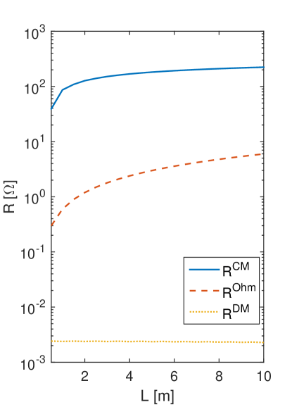
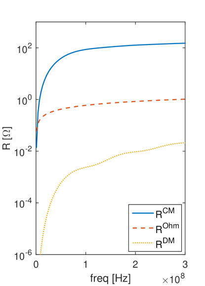
It is evident from the plots in Figure 1 that is some order of magnitude greater than , while this last one is also a couple of orders of magnitude smaller than . As for the radiation pattern of the power line cables, it is influenced by the load at the end of the line. When we consider a PLN, the load can be a line termination or the equivalent network impedance at a branch node. A matched load causes the propagation of the sole as a traveling wave. In this case most of the radiation is directed to the forward direction, with a main lobe pointing to an angle over the propagation axis. For longer cables, and the amplitude of the main lobe tend to decrease and increase respectively. In the case of unmatched loads, both and propagate and their radiation effects sum up. Hence, two main lobes are created in the forward and backward directions, their amplitude being proportional to the square of the forward and reverse currents respectively.
The results presented in this section extend to TL with finite length L what has already been pointed out for infinitesimal dipoles in [14]: even CM currents with much lower magnitude than DM currents can produce a similar or even greater radiation. Moreover, any CM current traveling along a cable is deeply attenuated within few meters and its power is radiated instead of being conducted. Hence, it is important in PLC to study how both CM and DM propagate throughout the network, and how different mechanisms lead to CM-DM or DM-CM conversion, which eventually deeply influence the attenuation and the distortion of the communication signals.
II-A Radiation model for a two-wire transmission line
Following the results of the previous section, we herein extend the classical MTL PUL equivalent circuit [15] for a 3-wire cable to include also the equivalent radiation resistances.
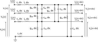
Figure 2 shows a line section of four conductors of length , where denote the PUL resistance, conductance, and capacitance of cable . The mutual inductance, capacitance and conductance take into account the mutual interactions between conductors. The bottom conductor is assumed to model a reference conductor, while the other three conductors represent the wires (i.e. Neutral, Phase and Protective Earth) that constitute the power line. We assume the ground, which normally has finite resistance, to be the reference conductor. With this model it is not only possible to analyze the differential transmission between two of the three conductors, but also to analyze the common mode transmission effects on the power line. In fact, by considering the MTRL PUL equivalent circuit, the series resistances do not only represent the ohmic losses but also the radiation losses as follows:
| (7) |
| (8) |
| (9) |
| (10) |
where , and are the conductors wrapped into the cable and is the reference ground. With this model, a series resistance for each wire accounts for the radiation losses due to differential signaling between that wire and another one. Moreover, a series resistance on the ground reference accounts for the radiation losses due to the common mode signaling that passes through the cable and closes its path through the ground.
In order for such a model to be extendible to a cable of any length, some simplifications need to be made for the models of and , since they do not increase linearly with the cable length. As for , we can consider to be equal to , where is the total DM radiation resistance of a semi-infinite cable, up to . This is because, as shown in Section II, the value of can be considered a constant function of for . For what matters , its trend with the line length is logarithmic. Hence, can be approximated with a piecewise constant value in order to correspond to a with a piecewise linear trend. The number of approximation segments has to be chosen based on a trade-off between the computational complexity and the desired accuracy of the results.
III Mode conversion and discontinuities
In this section, we explain the causes of mode conversion in power line networks, which eventually foster electromagnetic radiation and deteriorate the quality of the signal transmitted through the power line.
The main source of mode conversion in any electric or electronic circuit is system imbalance. Perfectly symmetric cables, circuits and loads would allow an independent transmission of CM and DM signals. While in integrated circuits advanced design strategies permit the physical minimization of mode conversions, few can be done in PLN, since there is no control on the wiring infrastructure, and only the load impedances corresponding to the power line modems can be optimized. Hence, the task of PLC engineers is not much about the minimization of the asymmetries, but it is more about the understanding of mode conversion and the derivation of a phenomenological characterization of it. As a result, new communication algorithms can be developed so that maximum throughput can be achieved yet respecting EMC norms.
We can distinguish between two types of mode conversion that occur in different parts of the network: mode conversion at the interface between the coupler of the power line modem (PLM) and the network, and mode conversion along the network.
III-A Coupler-network mode conversion
In PLM, unwanted common mode transmission is mostly caused by an unbalance between the conductors on the chip, given by asymmetrical grounding of the traces, or by finite impedance connection between different ground planes [16]. Although the design of modern modems allows to produce almost perfectly balanced differential signals, the connection to a long wire antenna like a power line branch causes CM-to-DM conversion. This conversion is due to parasitic coupling between the integrated circuit (IC) and the TL, and to the non-idealities of the coupling transformer. In particular, differential currents in the IC generate magnetic fields that can couple to the TL and generate a CM voltage. Also differential voltages in the IC can generate a CM current on the TL due to capacitive coupling [17].
Similarly, the magnetic field generated by the coupling transformer can impinge upon nearby traces and cables, and the parasitic capacitance between the primary and the secondary acts as a bypass for any CM noise.
III-B Conversions along the network
PLNs are characterized by many sources of unbalance, since many are the devices that constitute the network: power cables, junction boxes, power strips, plugs, sockets and the devices therein branched. Some of the common mechanisms giving rise to mode conversion have already been analyzed in the literature [18, 19, 20] and we present them below.
III-B1 Conversion to common mode along the line
A typical power line cable, in both longitudinal and transverse directions, is far from being regular and uniform. Differences in the dielectric material thickness, radius of the copper conductor, relative position of the cables, are usual in this type of network. Also simple cable bends can perturb the symmetry of a line. Each of these discontinuities results in a localized variation of the cable electrical characteristics, which produces mode conversion.
Moreover, inside junction boxes, power strips, plugs and sockets, the three conductors of a power line are generally unwrapped from the outer sheath. The different conductors are then differently warped and also cut at different lengths before being connected to the junction.
A final source of mode conversion is the difference in ground potentials. Also in indoor environments the ground is characterized by a finite resistance at high frequencies, which fosters the generation and propagation of CM currents.
III-B2 Unbalance at the load
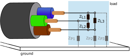
Any network load can be represented by the impedances , and connected at a line termination, as depicted in Figure 3. Moreover, the coupling between the lines and the ground is modeled with three parasitic impedances . If the impedances of the common mode paths are different then part of the DM current will flow through the common mode path. This phenomenon reduces the power available at the load and generates common mode currents. Conversely, the same imbalance also causes CM to generate DM currents, which might corrupt the transmitted DM signal. The imbalance can be caused by different types of couplings between the load and the ground or other objects in the proximity of the load [21].
IV Power Line Network Model
Given the MTRL PUL model presented in Section II-A and the considerations about mode conversion done in Section III, we can now introduce a model to study the effect of signal radiation and mode conversion on a generic PLN. First, we rely on the MTL theory to describe the propagation of CM and DM signals along each power line cable. The relations between signals at the two edges of a cable is then described using a mixed-mode scattering matrix (MMSM). MMSMs are also used to characterize all the other devices and loads present in a PLN. By converting the MMSMs to transmission matrices (MMTMs), it is then possible to use the chain rule and represent the whole PLN connecting any two network nodes by a single equivalent MMTM, from which the modal transfer functions can be computed. We point out that scattering and transmission matrices are here only used for convenience, since high-frequency characterization is usually performed with vector network analyzers that measure scattering parameters. The entire network can be equivalently represented in terms of voltages and currents. The fundamental concept is here to use a mixed-mode representation in order to characterize both DM and CM.
In the following, we summarize the theory about scattering matrices, MMSMs and MMTMs and the conversion equations between each representation.
IV-A Three-conductor and earth transmission line equations
In order to provide a steady-state analysis, we use the phasor representation for the electrical quantities. We denote for , where are the labels for the three conductors, the voltage phasor associated with the generator circuit and the receiver circuit at a frequency and coordinate . To simplify the notation, we do not explicitly show the frequency dependency in the following. Solving the Kirchhoff equations for the PUL circuit represented in Figure 2 and letting , provides the telegraph equations [15]
| (11) | ||||
| (12) |
where is the voltage phase vector, is the current phasor vector, and denotes the transposition operator.
Furthermore,
are the PUL parameters matrices for the resistance, inductance, capacitance and conductance, respectively. We remark that includes both the ohmic and radiation resistances. Solving (12) as presented in [10] gives the voltage and current propagation equations
| (14) |
where and are the propagation constant and the characteristic impedance of the cable respectively. is a known transformation matrix and , where is the reflection coefficient given by the load as
| (15) |
IV-B MTL scattering matrix
A power line branch can be in general represented as a multiport system where the signal at N input ports is transferred to N output ports. To derive the scattering matrix of this system, (14) has to be solved for and , where is the length of the line, respectively. The voltages and currents at the input side of the MTL are
| (16) | ||||
| (17) |
while the voltages and currents at the output side of MTL are
| (18) | ||||
| (19) |
The subscripts and denote the input and output ports respectively. In order to solve these equations, it is necessary to introduce the impedance matrices and at the input and the output of the line respectively. These impedance matrices provide a boundary condition through (15) to the system and allow it to be solved.
The resulting scattering matrix is a 2N x 2N matrix, partitioned in 4 NxN matrices as
| (20) |
where is the auto-scattering matrix of the inputs, is the auto-scattering matrix of the outputs, and and are the transition scattering matrices from the inputs to the outputs and vice versa. The complete derivation of the scattering matrix (20) is presented in [22].
IV-C Mixed-mode scattering matrix
In order to improve the understanding of the signal propagation through a transmission line, can be redefined to explicitly show the relation between differential and common modes, using the theory of the mixed-mode scattering matrix (MMSM) [23].
The single-ended generic port is defined by the single-ended voltage and current state vector:
| (21) |
where the symbol indicates the transpose operator.
On the other hand, the mixed-mode generic port with , , where M is the total number of ports, is defined based on the single-ended voltages and currents as:
| (22) |
where the indicates the differential voltages and currents and the symbol indicates the common mode ones. The corresponding mixed-mode voltage and current state vector is:
| (23) |
After defining the complex reference impedance as , the forward and reverse pseudowaves for the single-ended ports are defined as:
| (24) |
A pseudowave state vector of two single-ended ports can be defined as:
| (25) |
For the mixed-mode ports, the reference impedances are defined as and for the DM and CM respectively. The mixed-mode pseudo waves are therefore defined as:
| (26) |
A pseudowave state vector of a single mixed-mode port can be defined as:
| (27) |
Using eqs. 22, 24 and 26, the relation between single-ended and mixed-mode pseudowaves state vectors becomes
| (28) |
where is reported in (29).
| (29) |
If , then the matrix becomes [24]:
| (30) |
The scattering matrix for single-ended ports and for mixed-mode ports obey the following relations
| (31) |
where , , , .
Reordering the rows of , it is possible to compute the relationship between the mixed-mode scattering matrix and the single-ended scattering matrix . To this aim, is split in two rectangular matrices . is composed by the first two rows of and the last two, respectively. A new matrix is made by exchanging the position of and so that
| (32) |
Finally, from (32),(31), the direct and inverse transformations linking and are:
| (33) | |||
| (34) |
where and are defined as
| (35) |
and is the 2x2 identity matrix.
The matrix is a 2x2 matrix, with the following parameters: denoting the differential mode, denoting the common mode and as well as denoting the conversion between both modes.
| (36) |
The final scattering matrix respectively for the single-ended and mixed-mode ports are
| (37) |
where , , and . The conversion between and is computed by applying (34) and to all the possible couples.
IV-D Mixed-mode transmission matrix
The description of MTL blocks with the mixed-mode scattering matrix helps to understand the conversion between DM and CM and vice versa. A drowback of the scattering parameters is that they do not allow to easily manipulate the concatenation of multiple scattering matrices. However, MMSMs can be converted to mixed-mode transmission matrices (MMTMs) [24]. The system resulting from the connection of devices can be represented by a MMTM that is given by the multiplication of the MMTMs of the single subsystems.
The conversion procedure comprises: repositioning of the matrix parameters and a linear transformation. The ports should be repositioned in order to reach this form: where , ; where , , where subscripts and refer to the input and output side of the network (see Figure 4).
The following linear transformation then applies:
| (38) |
Where,
| (39) | ||||
| (40) | ||||
| (41) | ||||
| (42) |

V Application to power line networks
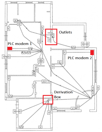
Power line networks as the one depicted in Figure 5 are composed by a mixture of different appliances connected by cables that often have different characteristics in different branches [25]. Moreover, cable interconnections include junction boxes, power strips, plugs and sockets that increase the network complexity. In order to account for all of these elements when simulating the communication between two PLMs, an equivalent MMTM representation for each element has to be provided. All these matrices are combined using the chain rule [26] to compute the total channel frequency response.

As for the cables, we represent them using the results reported in Section IV-B. We decided to use four input and four output single-ended ports to describe each MTRL block. This configuration is converted in two input and two output mixed-mode ports (see Figure 4). The defined number of ports has been chosen to obtain a squared shape for the final mixed-mode matrix. The square matrix is easily manipulated for the final conversion to the transmission mixed-mode scattering matrix. Moreover, MIMO PLMs usually communicate through two transmit ports, since only two linearly independent voltage differences can exist between the three conductors of a power line cable. Hence, it make sense to consider the whole PLN to be composed by two input and two output elements.
Using the same approach, each network load can be also represented with a 4-port configuration, as depicted in Figure 6, which allows a separate representation of the DM and CM impedances. We point out that in Section IV-B is different for different type of loads. In fact, while three phase loads are entirely characterized by , single phase loads can be simply described by one of the three impedances , while the other two account for parasitic effects. Finally, PLMs impose two DM impedances on the network termination. The matrix of each load can be in general computed referring to Figure 6. In this paper, we report the result obtained for a single phase load characterized by . The scattering matrix referred to is
| (43) |
where
| (44) | ||||
| (45) | ||||
| (46) | ||||
| (47) | ||||
| (48) | ||||
| (49) |
and are the reference impedances at port 1…4 respectively and is the parallel resistance operator.
VI Measurements results
In this section, we present measurement results used to justify the need of a mixed-mode cable representation in PLNs.
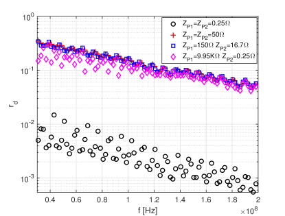
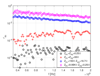
Our setup is made by a three wire 10 m long power line cable Artic Grade 3183YAG 3x1.5 mm. After measuring its MMSM using a vector network analyzer, we terminated the cable with a load between conductors 1 and 2 having and different values of and . By cascading the cable and load MMSMs, we obtained an equivalent MMSM that has been analyzed as reported in the following.
Assuming to inject only a differential signal between conductors 1 and 2 (corresponding to the mixed-mode port , see Figure 4), the ratio between the input and output differential power can be computed as
| (50) |
while the ratio between the input power and the common mode output power is:
| (51) |
The complex power at the port either for the DM or the CM is computed using the relation
| (52) |
where is the complex conjugate operator.
Figure 7 depicts the frequency trend of for different values of and . Circles and plus symbols are used to represent the results for balanced loading with 0.25 and 50 respectively. Square symbols represent the results for 150 and 16.7 , while diamond symbols represent the results for 9.95 k and 0.25 . When , the low values of are only due to ohmic and radiation losses. The impedance imbalance represented by the square symbols does almost not affect the DM transmission, while the reduction of the value of becomes evident only for extreme imbalances (diamond symbols). Finally, when both and have very low values (circles), DM transmission is significantly reduced.
Figure 8 depicts the frequency trend of for different values of and . While the two cases with exhibit very low values of , the mode conversion is significantly higher for . This confirms that, when the CM load is balanced, the measured mode conversion is due to little imbalances internal to the cable, while when the CM load is unbalanced, the load asymmetry effect dominates on the overall mode conversion. Moreover, the greater the load imbalance is, the greater is the power transfer from differential to common mode. In fact, a comparison between Figure 7 and Figure 8 shows that the power converted to CM when 150 and 16.7 (square symbols) is about one order of magnitude less than the transmitted differential power. Conversely, when 9.95 k and 0.25 (diamond symbols) so that the CM loads are more unbalanced, the transferred power is almost equally split between differential and common mode.
VII Conclusions
In this paper, we presented a novel power line network model that takes into account the effect of EMI and also mode conversions occurring along the medium on the signal transfer function. We firstly showed that radiation in PLC occurs at the network discontinuities and its radiation pattern depends on the length of each branch. The electro magnetic radiation of the cables is accounted in the PUL equivalent circuit of the MTRL by a series resistance for each wire. Since the radiation due to CM signals is much prominent than radiation due to DM signals, we proposed to describe each element of a PLN with its equivalent MMSM, which accounts for mode conversions. By cascading the MMTM blocks corespondent to each cable section and each device/load, the overall PLN connecting any two nodes can be represented by an equivalent MMTM. We showed that such matrix can be used to compute the overall mode conversion of the network and we tested our model measuring the mode conversion of a loaded cable. The results of this paper open a path for future research endeavors that will be directed towards the development of a comprehensive power line network simulator that incorporates conducted and radiated phenomena.
References
- [1] L. Lampe, A. M. Tonello, and T. G. Swart, Eds., Power Line Communications: Principles, Standards and Applications from Multimedia to Smart Grid. Wiley, 2016.
- [2] L. T. Berger, A. Schwager, P. Pagani, and D. Schneider, MIMO Power Line Communications: Narrow and Broadband Standards, EMC, and Advanced Processing. Boca Raton, FL, USA: CRC Press, Inc., 2014.
- [3] C. J. Kikkert, “Calculating radiation from power lines for power line communications,” in MATLAB for Engineers - Applications in Control, Electrical Engineering, IT and Robotics, D. K. Perutka, Ed. Intech, 2011, ch. 9.
- [4] A. Mescco, P. Pagani, M. Ney, and A. Zeddam, “Radiation mitigation for power line communications using time reversal,” Journal of Electrical and Computer Engineering, vol. 2013, 2013.
- [5] M. Girotto and A. M. Tonello, “EMC regulations and spectral constraints for multicarrier modulation in plc,” IEEE Access, vol. 5, pp. 4954–4966, 2017.
- [6] H. Haase, T. Steinmetz, and J. Nitsch, “New propagation models for electromagnetic waves along uniform and nonuniform cables,” IEEE Transactions on Electromagnetic Compatibility, vol. 46, no. 3, pp. 345–352, Aug 2004.
- [7] R. Ianconescu and V. Vulfin, “Free space TEM transmission lines radiation losses model,” 2017. [Online]. Available: https://arxiv.org/abs/1701.04878
- [8] D. M. Pozar, Microwave Engineering – Fourth Edition. John Wiley & Sons, 2011.
- [9] H. Erkens and H. Heuermann, “Mixed-mode chain scattering parameters: Theory and verification,” IEEE Transactions on Microwave Theory and Techniques, vol. 55, no. 8, pp. 1704–1708, Aug 2007.
- [10] F. Versolatto and A. Tonello, “An MTL theory approach for the simulation of MIMO power-line communication channels,” IEEE Transactions on Power Delivery, vol. 26, no. 3, pp. 1710–1717, 2011.
- [11] A. T. de Hoop, Handbook of radiation and scattering of Waves. Academic Press, 2008, ISBN: 0-12-208655-4.
- [12] C. A. Balanis, Antenna Theory: Analysis and Design. Wiley-Interscience, 2005.
- [13] C. Walter, Traveling wave antennas, ser. McGraw-Hill electronic science series. McGraw-Hill, 1965.
- [14] C. R. Paul and D. R. Bush, “Radiated emissions from common-mode currents,” in 1987 IEEE International Symposium on Electromagnetic Compatibility, Aug 1987, pp. 1–7.
- [15] C. R. Paul, Analysis of Multiconductor Transmission Lines, 2nd ed. Wiley-IEEE Press, 2007.
- [16] D. M. Hockanson, J. L. Dreniak, T. H. Hubing, T. P. van Doren, F. Sha, and C.-W. Lam, “Quantifying EMI resulting from finite-impedance reference planes,” IEEE Transactions on Electromagnetic Compatibility, vol. 39, no. 4, pp. 286–297, Nov 1997.
- [17] D. M. Hockanson, J. L. Drewniak, T. H. Hubing, T. P. V. Doren, F. Sha, and M. J. Wilhelm, “Investigation of fundamental EMI source mechanisms driving common-mode radiation from printed circuit boards with attached cables,” IEEE Transactions on Electromagnetic Compatibility, vol. 38, no. 4, pp. 557–566, Nov 1996.
- [18] A. Vukicevic, M. Rubinstein, F. Rachidi, and J. L. Bermudez, “On the mechanisms of differential-mode to common-mode conversion in the broadband over power line (BPL) frequency band,” in 2006 17th International Zurich Symposium on Electromagnetic Compatibility, Feb 2006, pp. 658–661.
- [19] F. Arteche and C. Rivetta, “Effects of CM and DM noise propagation in LV distribution cables,” 2003. [Online]. Available: https://cds.cern.ch/record/722106
- [20] L. Niu and T. Hubing, “Modeling the conversion between differential mode and common mode propagation in transmission lines,” 2015. [Online]. Available: http://www.cvel.clemson.edu/Reports/CVEL-14-055.pdf
- [21] “Appendix G: Coupling of EMI to cables: theory and models,” in Electromagnetic Compatibility Aspects Of Future Radio-Based Mobile Telecommunication Systems, L. P. C. Programme, Ed. Intech, 1999. [Online]. Available: http://www.emc.york.ac.uk/reports/linkpcp/
- [22] D. Kajfez, “Multiconductor transmission lines,” 1972. [Online]. Available: http://ece-research.unm.edu/summa/notes/In/0151.pdf
- [23] D. E. Bockelman and W. R. Eisenstadt, “Combined differential and common-mode scattering parameters: theory and simulation,” IEEE Transactions on Microwave Theory and Techniques, vol. 43, no. 7, pp. 1530–1539, Jul 1995.
- [24] A. Ferrero and M. Pirola, “Generalized mixed-mode s-parameters,” IEEE Transactions on Microwave Theory and Techniques, vol. 54, no. 1, pp. 458–463, Jan 2006.
- [25] A. Tonello and F. Versolatto, “Bottom-up statistical PLC channel modelling - part I: Random topology model and efficient transfer function computation,” IEEE Transactions on Power Delivery, vol. 26, no. 2, pp. 891–898, Apr. 2011.
- [26] S. Galli and T. Banwell, “A novel approach to the modeling of the indoor power line channel-part II: transfer function and its properties,” IEEE Transactions on Power Delivery, vol. 20, no. 3, pp. 1869–1878, July 2005.