Indirect excitons in van der Waals heterostructures at room temperature
Abstract
Indirect excitons (IXs) in van der Waals transition-metal dichalcogenide (TMD) heterostructures are characterized by a high binding energy making them stable at room temperature and giving the opportunity for exploring fundamental phenomena in excitonic systems and developing excitonic devices operational at high temperatures. We present the observation of IXs at room temperature in van der Waals TMD heterostructures based on monolayers of MoS2 separated by atomically thin hexagonal boron nitride. The IXs realized in the TMD heterostructure have lifetimes orders of magnitude longer than lifetimes of direct excitons in single-layer TMD, and their energy is gate controlled.
pacs:
73.63.Hs, 78.67.De, 05.30.JpAn indirect exciton (IX) is composed of an electron and a hole confined in spatially separated quantum well layers. IXs can be realized in coupled quantum well (CQW) semiconductor heterostructures. Long lifetimes of IXs allow them to cool below the temperature of quantum degeneracy Lozovik1976 ; Butov2001 . Experimental studies of degenerate Bose gases of IXs were performed so far in GaAs CQW structures where quantum degeneracy was achieved in the temperature range of few Kelvin. The findings include spontaneous coherence and condensation of excitons High2012 , long-range spin currents and spin textures High2013 , spatially modulated exciton state Yang2015 , and perfect Coulomb drag Nandi2012 . Furthermore, IX energy, lifetime, and flux can be controlled by voltage that is explored for the development of excitonic devices. Excitonic devices with IXs were demonstrated so far at temperatures below K. These devices include traps, lattices, conveyers, and ramps, which are used for studying basic properties of cold IXs, as well as excitonic transistors, routers, and photon storage devices, which hold the potential for creating excitonic signal processing devices and excitonic circuits, a review of excitonic devices can be found in Butov2017 .
A finite exciton binding energy limits the operation temperature of excitonic devices. Excitons exist in the temperature range roughly below ( is the Boltzmann constant) Chemla1984 . Furthermore, the temperature of quantum degeneracy, which can be achieved with increasing density before excitons dissociation to electron-hole plasma, also scales proportionally to Fogler2014 . These considerations instigate the search for material systems where IXs have a high binding energy and, as a result, can provide the medium for the realization of high-temperature coherent phenomena and excitonic devices.
IXs were explored in various III-V and II-VI semiconductor QW heterostructures based on GaAs Butov2001 ; High2012 ; High2013 ; Yang2015 ; Nandi2012 ; Butov2017 ; Chemla1984 ; Islam1987 ; Alexandrou1990 , AlAs Zrenner1992 ; Grosso2009 , InGaAs Butov1995 , GaN Lefebvre2004 ; Fedichkin2015 ; Fedichkin2016 , and ZnO Morhain2005 ; Kuznetsova2015 . Among these materials, IXs are more robust in the ZnO structures where their binding energy is about 30 meV Morhain2005 . Proof of principle for the operation of IX switching devices was demonstrated at temperatures up to K in AlAs/GaAs CQW Grosso2009 where the IX binding energy is about meV Zrenner1992 . Studies of IXs in III-V and II-VI semiconductor materials continue to attract intense interest.
Van der Waals structures composed of atomically thin layers of transition metal dichalcogenides (TMD) offer an opportunity to realize artificial materials with designable properties, forming a new platform for studying basic phenomena and developing optoelectronic devices Geim2013 . TMD heterostructures allow IXs with remarkably high binding energies Fogler2014 ; Ye2014 ; Chernikov2014 , much higher than in III-V or II-VI semiconductor heterostructures. Therefore, IXs in TMD heterostructures open the opportunity to realize room-temperature excitonic devices and explore high-temperature quantum degenerate Bose gases of IXs.
The experimental approaches to the realization of IXs in TMD materials involve two kinds of heterostructures. In type I TMD heterostructures with direct gap alignment, the electron and hole layers are spatially separated by a barrier layer. Such type I structures with MoS2 forming the QW layers and a hexagonal boron nitride (hBN) forming the barrier were considered in Fogler2014 ; Calman2016 . These heterostructures are similar to GaAs/AlGaAs CQW heterostructures where GaAs forms QW layers and AlGaAs forms the barrier Butov2001 ; High2012 ; High2013 ; Yang2015 ; Nandi2012 ; Butov2017 ; Islam1987 ; Alexandrou1990 . In type II TMD heterostructures with staggered band alignment, the electron and hole layers form in different adjacent TMD materials such as single-layer MoSe2 and WSe2 Rivera2015 ; Rivera2016 ; Nagler2017 , MoS2 and WSe2 Fang2014 ; Latini2017 , MoS2 and WS2 Hong2014 ; Palummo2015 , MoSe2 and WS2 Bellus2015 , and MoS2 and MoSe2 Mouri2017 . These heterostructures are similar to AlAs/GaAs CQW heterostructures where electrons and holes are confined in adjacent AlAs and GaAs layers, respectively Zrenner1992 ; Grosso2009 .
Here, we report on the realization of IXs in type I TMD heterostructures at room temperature. This was achieved using the previously demonstrated approach with MoS2/hBN type-I CQW Calman2016 combined with an improved structure design and detected using time-resolved optical spectroscopy.
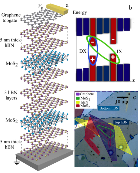
The structure studied here was assembled by stacking mechanically exfoliated two-dimensional crystals on a graphite substrate, which acts as a global backgate (Fig. 1a). The top view of the device showing the contours of different layers is presented in Fig. 1c. The CQW is formed where the two MoS2 monolayers, separated by three hBN layers, overlap. IXs are formed from electrons and holes in different MoS2 layers (Fig. 1b). The top and bottom 5 nm thick hBN serve as dielectric cladding layers. Voltage applied between the top graphene layer and the backgate is used to create the bias across the CQW structure. The thickness of hBN cladding layers is much smaller than in our previous CQW TMD device Calman2016 . This allowed us to achieve a much higher electric field across the structure for the applied voltage and, in turn, realize effective control of IX energy by voltage as described below.
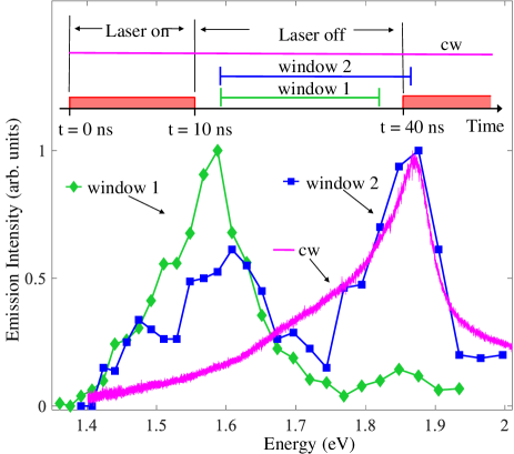
The excitons were generated by a semiconductor laser with excitation energy eV. In continuous wave (cw) experiments, photoluminescence (PL) spectra were measured using a spectrometer with resolution 0.2 meV and a liquid-nitrogen-cooled CCD. In all time-resolved experiments, the laser pulses had a rectangular shape with the duration 10–50 ns, period 40–200 ns, and edge sharpness ns (Fig. 2). The laser was focused to a m spot. In time-resolved PL kinetics and spectrum measurements, the emitted light was filtered by an interference filter or diffracted by the spectrometer, respectively, and then detected by a photomultiplier tube and time correlated photon counting system. In time-resolved imaging experiments, the emitted light was filtered by an interference filter and detected by a liquid-nitrogen-cooled CCD coupled to a PicoStar HR TauTec time-gated intensifier. The measurements were performed in a 4He atmosphere at room temperature ( K) and in a liquid 4He cryostat at 2 K.
IXs dominate the emission spectrum measured after the laser excitation pulse (Fig. 2). At the time delays exceeding the DX recombination times, most of DXs have recombined, and so the recombination of IXs, which have a much longer lifetime, is not masked by the DX recombination. Both short-lifetime DX and long-lifetime IX emission lines are observed in the spectrum measured in the time-window between the laser pulses and the first ns of the laser pulse (Fig. 2). As the fraction of time corresponding to the laser pulse grows, the relative intensity of the DX emission increases. In the cw regime, where the laser is permanently on, DXs dominate the spectrum due to their higher oscillator strength (Fig. 2).
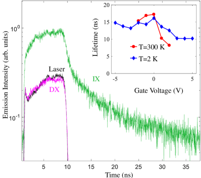
The IX emission kinetics is presented in Fig. 3. The time resolution of the experimental system including the pulse generator, the laser, the photomultiplier, and the time correlated photon counting system is approximately 0.5 ns as seen from the decay kinetics measured at eV. The DX decay kinetics measured at the DX line peak eV closely follows the excitation laser decay indicating that the DX lifetime is shorter than the 0.5 ns experimental resolution. The decay kinetics in the IX spectral range eV shows a double-exponential decay (Fig. 3). Its faster component is determined by the decay of low-energy DX states, which appear in the IX spectral range due to the spectral broadening of the DX line (Fig. 2). The slower component is determined by the IX decay (Fig. 3). The IX lifetime ns is orders of magnitude longer than the DX lifetime (Fig. 3) and is controlled by gate voltage over a range of several ns (Fig. 3 insert). The voltage dependence of the IX lifetime has two characteristic features. First, it reduces at positive where the IX energy approaches the DX energy (Fig. 5). Second, it has a local maximum around . Both these features were also observed for IXs in GaAs heterostructures Grosso2009 . The former can be attributed to the increase of the overlap of electron and hole wave functions with approaching the direct regime. The latter may result from the suppression of the leakage currents through the CQW layers at zero bias. The realization of the indirect regime, where the IXs are lower in energy than DXs, already at indicates an asymmetry of the device, presumably due to unintenional doping.
Regarding the physical mechanism that governs the IX lifetime in the studied heterostructure we can say the following. In general, this lifetime is limited by tunneling through the hBN spacer. However, direct tunneling across the entire thickness nm of the spacer should be prohibitively slow. The tunneling action and tunneling probability can be estimated to be and , respectively, assuming the potential barrier of height 2 eV and the carrier mass inside the barrier (similar to Fogler2014 ). Therefore, we surmise that the IX recombination involves transmission through some midgap defects in the spacer Britnell2012 .
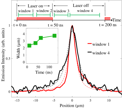
Figure 4 shows the spatial profiles of IX emission. The width of the emission profiles determined by a fit to Lorentzian distribution (dashed lines in Fig. 4) is shown in insert to Fig. 4 as a function of time. The emission profiles after the laser excitation pulse have wider spatial distributions than during the pulse. During the laser excitation pulse, the low-energy tail of short-lifetime DX emission strongly contributes to the emission in the IX spectral region (Fig. 2). After the pulse, DXs decay quickly and the emission is dominated by the long-lifetime IXs. Diffusion of IXs away from the laser excitation spot during their long lifetime contributes to the wider spatial profiles of IX emission. The increase in emission width after the pulse end can be used for estimating an upper bound on the IX diffusion coefficient . For m (Fig. 4) and IX lifetime ns (Fig. 3) this gives cm2/s.
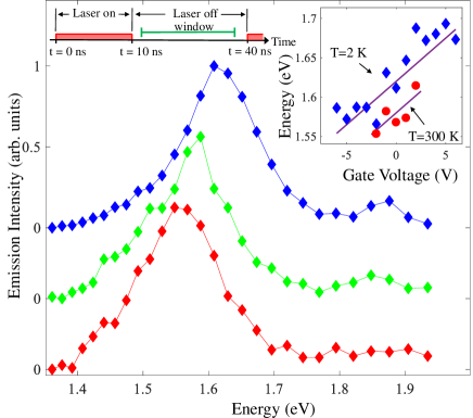
Figure 5 shows control of the IX energy by gate voltage. The energy of the long-lifetime emission line shifts by about 120 meV at cryogenic temperatures and by about 60 meV at room temperature. No leakage current or sample damage was detected at cryogenic temperatures in the measurements at applied voltages up to V, which is typical for thin hBN that can withstand electric fields of about 0.5 V/nm Britnell2012 . However, at room temperature, applying V led to the appearance of leakage current through the device and the reduced device resistivity persisted after lowering . This limited the maximum applied voltage and, in turn, the IX energy shift at room temperature.
In summary, IXs were observed at room temperature in van der Waals MoS2/hBN heterostructure. The IXs have long lifetimes, orders of magnitude longer than lifetimes of direct excitons in single-layer MoS2, and their energy is controlled by voltage at room temperature.
These studies were supported by DOE Office of Basic Energy Sciences under award DE-FG02-07ER46449 and NSF Grant No. 1640173 and NERC, a subsidiary of SRC, through the SRC-NRI Center for Excitonic Devices.
References
- (1) Yu.E. Lozovik, V.I. Yudson, A new mechanism for superconductivity: pairing between spatially separated electrons and holes. Sov. Phys. JETP 44, 389-397 (1976).
- (2) L.V. Butov, A.L. Ivanov, A. Imamoglu, P.B. Littlewood, A.A. Shashkin, V.T. Dolgopolov, K.L. Campman, A.C. Gossard, Stimulated Scattering of Indirect Excitons in Coupled Quantum Wells: Signature of a Degenerate Bose-Gas of Excitons, Phys. Rev. Lett. 86, 5608-5611 (2001).
- (3) A.A. High, J.R. Leonard, A.T. Hammack, M.M. Fogler, L.V. Butov, A.V. Kavokin, K.L. Campman, A.C. Gossard, Spontaneous coherence in a cold exciton gas, Nature 483, 584-588 (2012).
- (4) A.A. High, A.T. Hammack, J.R. Leonard, Sen Yang, L.V. Butov, T. Ostatnický, M. Vladimirova, A.V. Kavokin, T.C.H. Liew, K.L. Campman, A.C. Gossard, Spin currents in a coherent exciton gas, Phys. Rev. Lett. 110, 246403 (2013).
- (5) Sen Yang, L.V. Butov, B.D. Simons, K.L. Campman, A.C. Gossard, Fluctuation and commensurability effect of exciton density wave, Phys. Rev. B 91, 245302 (2015).
- (6) D. Nandi, A.D.K. Finck, J.P. Eisenstein, L.N. Pfeiffer, K.W. West, Exciton condensation and perfect Coulomb drag, Nature 488, 481-484 (2012).
- (7) L.V. Butov, Excitonic devices, Superlattices Microstruct. 108, 2-26 (2017).
- (8) D.S. Chemla, D.A.B. Miller, P.W. Smith, A.C. Gossard, W. Wiegmann, Room temperature excitonic nonlinear absorption and refraction in GaAs/AlGaAs multiple quantum well structures, IEEE J. Quantum Electron. 20, 265-275 (1984).
- (9) M.M. Fogler, L.V. Butov, K.S. Novoselov, High-temperature superfluidity with indirect excitons in van der Waals heterostructures, Nat. Commun. 5, 4555 (2014).
- (10) M.N. Islam, R.L. Hillman, D.A.B. Miller, D.S. Chemla, A.C. Gossard, J.H. English, Electroabsorption in GaAs/AlGaAs coupled quantum well waveguides, Appl. Phys. Lett. 50, 1098-1100 (1987).
- (11) A. Alexandrou, J.A. Kash, E.E. Mendez, M. Zachau, J.M. Hong, T. Fukuzawa, Y. Hase, Electric-field effects on exciton lifetimes in symmetric coupled GaAs/Al0.3Ga0.7As double quantum wells, Phys. Rev. B 42, 9225-9228 (1990).
- (12) A. Zrenner, P. Leeb, J. Schäfler, G. Böhm, G. Weimann, J.M. Worlock, L.T. Florez, J.P. Harbison, Indirect excitons in coupled quantum well structures, Surf. Sci. 263, 496-501 (1992).
- (13) G. Grosso, J. Graves, A.T. Hammack, A.A. High, L.V. Butov, M. Hanson, A.C. Gossard, Excitonic switches operating at around 100 K, Nat. Photonics 3, 577-580 (2009).
- (14) L.V. Butov, A. Zrenner, G. Abstreiter, A.V. Petinova, K. Eberl, Direct and indirect magnetoexcitons in symmetric InxGa1-xAs/GaAs coupled quantum wells, Phys. Rev. B 52, 12153-12157 (1995).
- (15) P. Lefebvre, S. Kalliakos, T. Bretagnon, P. Valvin, T. Taliercio, B. Gil, N. Grandjean, J. Massies, Observation and modeling of the time-dependent descreening of internal electric field in a wurtzite GaN/Al0.15Ga0.85N quantum well after high photoexcitation, Phys. Rev. B 69, 035307 (2004).
- (16) F. Fedichkin, P. Andreakou, B. Jouault, M. Vladimirova, T. Guillet, C. Brimont, P. Valvin, T. Bretagnon, A. Dussaigne, N. Grandjean, P. Lefebvre, Transport of dipolar excitons in (Al,Ga)N/GaN quantum wells, Phys. Rev. B 91, 205424 (2015).
- (17) F. Fedichkin, T. Guillet, P. Valvin, B. Jouault, C. Brimont, T. Bretagnon, L. Lahourcade, N. Grandjean, P. Lefebvre, M. Vladimirova, Room-Temperature Transport of Indirect Excitons in (Al,Ga)N/GaN Quantum Wells, Phys. Rev. Appl. 6, 014011 (2016).
- (18) C. Morhain, T. Bretagnon, P. Lefebvre, X. Tang, P. Valvin, T. Guillet, B. Gil, T. Taliercio, M. Teisseire-Doninelli, B. Vinter, C. Deparis, Internal electric field in wurtzite ZnO/Zn0.78Mg0.22O quantum wells, Phys. Rev. B 72, 241305(R) (2005).
- (19) Y.Y. Kuznetsova, F. Fedichkin, P. Andreakou, E.V. Calman, L.V. Butov, P. Lefebvre, T. Bretagnon, T. Guillet, M. Vladimirova, C. Morhain, J.-M. Chauveau, Transport of indirect excitons in ZnO quantum wells, Opt. Lett. 40, 3667-3670 (2015).
- (20) A.K. Geim, I.V. Grigorieva, Van der Waals heterostructures, Nature 499, 419-425 (2013).
- (21) Ziliang Ye, Ting Cao, Kevin O’Brien, Hanyu Zhu, Xiaobo Yin, Yuan Wang, Steven G. Louie, Xiang Zhang, Probing excitonic dark states in single-layer tungsten disulphide, Nature 513, 214-218 (2014).
- (22) Alexey Chernikov, Timothy C. Berkelbach, Heather M. Hill, Albert Rigosi, Yilei Li, Ozgur Burak Aslan, David R. Reichman, Mark S. Hybertsen, Tony F. Heinz, Exciton Binding Energy and Nonhydrogenic Rydberg Series in Monolayer WS2, Phys. Rev. Lett. 113, 076802 (2014).
- (23) E.V. Calman, C.J. Dorow, M.M. Fogler, L.V. Butov, S. Hu, A. Mishchenko, A.K. Geim, Control of excitons in multi-layer van der Waals heterostructures, Appl. Phys. Lett. 108, 101901 (2016).
- (24) Pasqual Rivera, John R. Schaibley, Aaron M. Jones, Jason S. Ross, Sanfeng Wu, Grant Aivazian, Philip Klement, Kyle Seyler, Genevieve Clark, Nirmal J. Ghimire, Jiaqiang Yan, D.G. Mandrus, Wang Yao, Xiaodong Xu, Observation of long-lived interlayer excitons in monolayer MoSe2-WSe2 heterostructures, Nat. Commun. 6, 6242 (2015).
- (25) Pasqual Rivera, Kyle L. Seyler, Hongyi Yu, John R. Schaibley, Jiaqiang Yan, David G. Mandrus, Wang Yao, Xiaodong Xu, Valley-polarized exciton dynamics in a 2D semiconductor heterostructure, Science 351, 688-691, (2016).
- (26) Philipp Nagler, Gerd Plechinger, Mariana V. Ballottin, Anatolie Mitioglu, Sebastian Meier, Nicola Paradiso, Christoph Strunk, Alexey Chernikov, Peter C.M. Christianen, Christian Schüller, Tobias Korn, Interlayer exciton dynamics in a dichalcogenide monolayer heterostructure, 2D Mater. 4, 025112 (2017).
- (27) Hui Fang, Corsin Battaglia, Carlo Carraro, Slavomir Nemsak, Burak Ozdol, Jeong Seuk Kang, Hans A. Bechtel, Sujay B. Desai, Florian Kronast, Ahmet A. Unal, Giuseppina Conti, Catherine Conlon, Gunnar K. Palsson, Michael C. Marting, Andrew M. Minor, Charles S. Fadley, Eli Yablonovitch, Roya Maboudian, Ali Javey, Strong interlayer coupling in van der Waals heterostructures built from single-layer chalcogenides, PNAS 111, 6198 (2014).
- (28) Simone Latini, Kirsten T. Winther, Thomas Olsen, Kristian S. Thygesen, Interlayer Excitons and Band Alignment in MoS2/hBN/WSe2 van der Waals Heterostructures, Nano Lett. 17, 938-945 (2017).
- (29) Xiaoping Hong, Jonghwan Kim, Su-Fei Shi, Yu Zhang, Chenhao Jin, Yinghui Sun, Sefaattin Tongay, Junqiao Wu, Yanfeng Zhang, Feng Wang, Ultrafast charge transfer in atomically thin MoS2/WS2 heterostructures, Nat. Nano 9, 682-686 (2014).
- (30) Maurizia Palummo, Marco Bernardi, Jeffrey C. Grossman, Exciton Radiative Lifetimes in Two-Dimensional Transition Metal Dichalcogenides, Nano Lett. 15, 2794-2800 (2015).
- (31) Matthew Z. Bellus, Frank Ceballos, Hsin-Ying Chiu, Hui Zhao, Tightly Bound Trions in Transition Metal Dichalcogenide Heterostructures, ACS Nano 9, 6459-6464, (2015).
- (32) Shinichiro Mouri, Wenjing Zhang, Daichi Kozawa, Yuhei Miyauchi, Goki Edac, Kazunari Matsuda, Thermal dissociation of inter-layer excitons in MoS2/MoSe2 hetero-bilayers, Nanoscale 9, 6674-6679 (2017).
- (33) L. Britnell, R.V. Gorbachev, R. Jalil, B.D. Belle, F. Schedin, A. Mishchenko, T. Georgiou, M.I. Katsnelson, L. Eaves, S.V. Morozov, N.M.R. Peres, J. Leist, A.K. Geim, K.S. Novoselov, L.A. Ponomarenko, Field-Effect Tunneling Transistor Based on Vertical Graphene Heterostructures, Science 335, 947-950 (2012).