Development of a compact EB microchannel plate detector for beam imaging
Abstract
A beam imaging detector was developed by coupling a multi-strip anode with delay line readout to an EB microchannel plate (MCP) detector. This detector is capable of measuring the incident position of the beam particles in one-dimension. To assess the spatial resolution, the detector was illuminated by an -source with an intervening mask that consists of a series of precisely-machined slits. The measured spatial resolution was 520m FWHM, which was improved to 413m FWHM by performing an FFT of the signals, rejecting spurious signals on the delay line, and requiring a minimum signal amplitude. This measured spatial resolution of 413m FWHM corresponds to an intrinsic resolution of 334m FWHM when the effect of the finite slit width is de-convoluted. To understand the measured resolution, the performance of the detector is simulated with the ion-trajectory code SIMION.
keywords:
microchannel plate detector , beam imaging , tracking detector , position-sensitive microchannel plate detector1 Introduction
A new generation of radioactive beam facilities provide unique opportunities to investigate nuclei far from -stability. However, the beam intensity of the most N/Z exotic nuclei is typically less than 1000 ions/s posing significant challenges in imaging these beams. In the case of low energy beams, it is particularly important that the imaging detector introduce the least amount of material into the beam path in order to minimally distort the beam. In addition, as most accelerator facilities are pulsed it is beneficial if the imaging detector has good timing characteristics. Due to their high gain, fast temporal response, sensitivity to a single electron, and compact size, microchannel plates (MCPs) are often used as an electron amplifier for these imaging detectors [1].
There are several methods for providing position sensitivity with an MCP detector including: multi-strip anode [2], helical delay line [3, 4], cross-strip anode [5], induced signal [6, 7], resistive anode [8, 9, 10], and Timepix CMOS readout [11]. To realize a beam imaging detector requires transport of electrons produced at a secondary-emission foil onto the surface of the position sensitive MCP detector situated away from the beam axis. In one approach, a clever magnetic field arrangement provided transport of the electrons on helical trajectories onto the the surface of a MCP detector [12, 13, 14]. This technique resulted in a spatial resolution of 588m FWHM [13]. The most serious limitation of this approach is the large space occupied by this detector making its use prohibitive in many experiments.
A beam timing detector which is compact and introduces a minimal amount of material into the beam path is an EB detector [15, 16, 17, 18]. Such a detector has been used to measure the time-of-flight of beam particles and reaction products in nuclear reaction studies [19, 20, 21]. To make the MCP in an EB detector position-sensitive we employed a multi-strip anode with delay line readout, which is a particularly appealing because of its simplicity and low cost. Moreover, due to the fast time response of the detector it is capable of resolving two particles that arrive simultaneously but are spatially separated. Two principal factors influence one’s ability to accurately image the beam: the impact of electron transport from the electron-emission foil to the MCP and the inherent spatial resolution of the position-sensitive element. In this article, we describe the design, development, and performance of an EB position-sensitive detector suitable for imaging low-intensity radioactive beams. We explore the impact of the electron transport for this detector geometry on the measured resolution using the ion trajectory code SIMION [22].
2 Experimental Setup
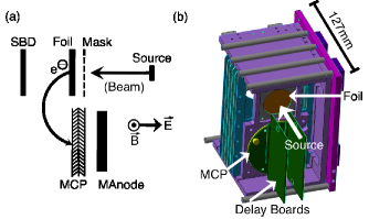
Presented in Fig. 1a is a schematic drawing of the experimental setup used to determine the spatial resolution of the position-sensitive EB MCP detector. Electrons, ejected from the 0.5m thick aluminized mylar foil by the passage of ionizing radiation, are accelerated and bent onto the surface of a 40mm diameter MCP. The MCP used was a standard chevron stack (APD 2 MA 40/12/10/12 60:1 NR) with 10m diameter microchannels provided by Photonis USA [23]. The MCP amplifies the incident electrons by a factor of 106. The resulting electron pulse is incident on a multi-strip anode. Printed on an FR4 PCB, the multi-strip anode is composed of 250m wide strips with a 75m inter-strip isolation. The total active area of the anode is 3cm x 3cm (w x h), thus restricting detection of the electrons amplified by the MCP. This choice of a reduced size anode was simply due to ease of implementation in an existing setup. It served the purpose of demonstrating the feasibility of the technique. All 100 strips of the anode are read out by two independent delay boards (as indicated in Fig. 1b) to read out the even and odd strips. The use of two delay boards minimizes the attenuation and dispersion experienced by the signal in the delay line. The delay boards consist of a continuous 7771mm long trace on a 10 layer Rogers 4350 PCB with 1ns/tap. Construction of the delay line with a high quality PCB material is essential to minimize signal degradation. The position of the incident particle is measured by constructing the time difference of the signal arrival at each end of the delay line. In prior work we used a multi-strip anode coupled to a delay line with a simple electrostatic arrangement [6, 9] to achieve a spatial resolution of 94m FWHM [24]. Any variation in the electron transport can only adversely impact this resolution. This delay line approach has been successfully employed at rates up to 10MHz [25].
A CAD drawing of the detector is presented in Fig. 1b. The electric field is produced using a series of rings situated co-axially along the beam path. By applying a voltage of +4500V to the most upstream ring plate (with 8mm between ring plates) and stepping the voltage down using 500M resistors between each ring an electric field of 114,300 V/m is generated. A magnetic field perpendicular to the beam axis is produced by a set of 8 neodymium permanent magnets [26]. The magnets each measure 25mm x 25mm x 12mm and are located on two soft iron plates measuring 146mm x 127mm x 98mm, and collectively produce a field of 90G in the region of electron production. This magnetic field bends the path of the electrons 180∘ onto the front face of the MCP. The impact energy of the electron on the MCP is controlled by biasing the aluminized mylar foil to -1250V. The biases of the foil and the ring plates were chosen to optimize the measured resolution. The front of the chevron MCP was held at ground, while the back of the chevron MCP was biased to +1792V. The multi-strip anode, spaced from the back of the MCP by 1mm, was biased to +2350V.
3 Measuring the Spatial Resolution of the EB MCP Detector
To test the performance of the detector, it was placed in a vacuum chamber that was evacuated to a pressure of 4 x 10⁻⁷ torr and illuminated by a 1.5Ci 241Am -source. Between the -source and the secondary-emission foil was a 0.8mm thick aluminum plate with 355m wide slits that are 6.4mm long. The 13 slits in the mask have a center-to-center spacing of 2mm. Alpha-particles passing through the mask and foil were detected using a silicon surface barrier detector (SBD) as shown in Fig. 1a.
Passage of an -particle through the foil generates electrons, which are transported by the EB field onto the MCP. The amplified electron signal from the MCP is incident on the multi-strip anode. A signal arriving on a strip propagates to the delay line, where it splits. The signals arriving at either end of the delay line are designated Yup and Ydown, and are used to determine the position of the incident particle. Each of these signals was amplified by a fast-timing preamplifier with a gain of 200 (Ortec VT120A) before being digitized by a 10GS/s waveform digitizer with 8 bit resolution (Tektronix DPO5204 oscilloscope). The digitizer was triggered using a coincidence between the MCP signal and the SBD signal in order to reduce background events due to radiogenic decays in the MCP. The MCP signal used for the trigger was first inverted with a 100MHz inverting transformer and subsequently amplified by an Ortec VT120A. The SBD (Ortec BA-45-900-100) was amplified by a fast preamplifier [27]. Both the MCP and SBD signals were discriminated using a constant-fraction discriminator (Tennelec TC454) before forming the coincidence.
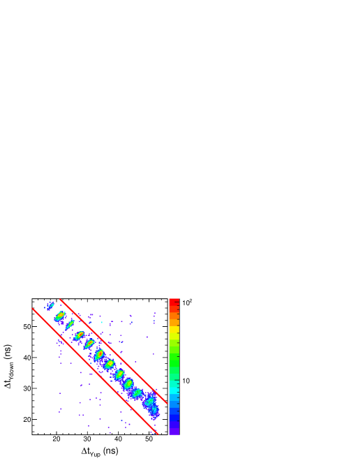
The arrival time of the Yup and Ydown signals is determined by utilizing a software constant-fraction discriminator (CFD), with a fraction of 0.5. A delay time of 1.5ns was chosen for the CFD based on the typical 3ns risetime of the signals. The time difference between the trigger time and the zero-crossing point of the CFD for the delay-line signals are designated tYup and tYdown.
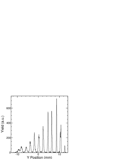
The two-dimensional correlation between tYup and tYdown is shown in Fig. 2. The majority of the data in Fig. 2 lies in a single anti-correlated band, with tYup increasing as tYdown decreases. The behavior is approximately linear indicating that dispersion and attenuation in the delay line do not play a significant role in distorting the time correlation. The anti-correlation results from the constant length of the delay line. Points that lie off this line are consequently spurious and can be rejected. One can clearly resolve twelve peaks in the spectrum which correspond to the slits in the mask. From the two-dimensional spectrum evident in Fig. 2, a one-dimensional spectrum, tYdown - tYup, is constructed. This spectrum is calibrated using the 2mm center-to-center spacing of the slits. The result is depicted in Fig. 3. The average width of the central 7 peaks in the spectrum, , was utilized to determine the spatial resolution. Based on the Gaussian-like nature of the peaks, the average FWHM was calculated using FWHM=2.35*. Using this approach the spatial resolution of the detector was determined to be 520m FWHM. An improvement was made by applying a Fast Fourier Transform (FFT) filter with a cutoff frequency of 150MHz. This improved the spatial resolution to 488m FWHM. The spatial resolution was further improved by selecting events with 70ns (tYdown + tYup) 80ns as indicated by the solid lines in Fig. 2. With this requirement the spatial resolution improved somewhat to 482m with a rejection of 8 of the events. Further requirement that the amplitude of the delay line signals exceeded -50mV resulted in the best resolution obtained. Collectively these selection criteria are referred to as the “clean condition” and resulted in a resolution of and 413m FWHM. Imposing this condition resulted in a rejection of 66 of the total events.
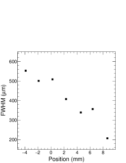
The dependence of the measured resolution on position is presented in Fig. 4 for signals which meet the selection criteria of the “clean condition”. A clear general trend is evident with the resolution decreasing from approximately 550 m to approximately 200 m over a distance of approximately 12 mm. The poorer resolution is associated with the location on the MCP furthest from the foil. This trend was qualitatively discernible in Fig. 3. Relaxing the amplitude requirement results in the same overall trend with a slightly larger resolution from 697 to 249 m.
4 Intrinsic Spatial Resolution of EB MCP Detector
The spatial resolution measured corresponds to the convolution of the intrinsic spatial resolution of the detector with the finite slit width. The measured resolution is given by:
| (1) |
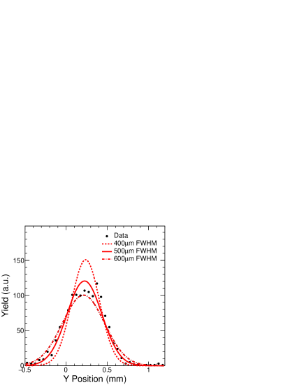
where is taken as a step function with a width of 355m to represent the slit, and is a Gaussian with the intrinsic width, . For a given intrinsic width the measured resolution can be calculated. By varying the intrinsic width, the relationship between intrinsic resolution and measured resolution can be established. This relationship allows one to relate the experimentally measured resolution to the intrinsic resolution. In Fig. 5, superimposed on the experimental data are the predicted resolutions, M(Y’), of 400m, 500m, and 600m FWHM. From this comparison, one can clearly deduce that the measured spatial resolution for this slit is consistent with approximately 500m FWHM. To extract an average intrinsic resolution, the effect of the finite slit width was de-convoluted from the measured resolution for each of the central 7 peaks. The extracted intrinsic resolution of each of the individual peaks was then averaged. Using this approach an average intrinsic resolution of 334m FWHM was determined. The measured resolutions for different selection and anaysis criteria along with the intrinsic resolution are summarized in Table 1.
| FWHM (m) | |
|---|---|
| Raw | 520 |
| FFT | 488 |
| FFT + Delay | 482 |
| FFT + Delay + 50mV | 413 |
| Intrinsic (FFT + Delay + 50mV ) | 334 |
5 Simulating the detector resolution
The significantly larger spatial resolution of 520 m obtained with the ExB detector as compared to the 94 m [24] associated with the simple electrostatic arrangement [6, 9] indicates that the electron transport from the foil to the MCP dictates the measured resolution. To understand the electron transport in the crossed electric and magnetic fields between the secondary-emission foil and the front surface of the MCP detector we simulated the electron trajectories using the ion trajectory code SIMION [22]. Performing these calculations required mapping the magnetic field accurately as described below.
5.1 Mapping the Magnetic Field
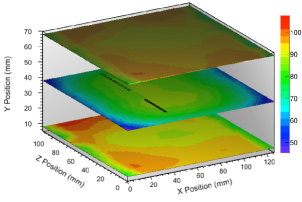
The magnetic field in the active detector volume was measured using the DC Gaussmeter model GM1-ST [28]. This probe has a manufacturer quoted resolution of 0.1G and an accuracy of 1 of the measured value. This probe was capable of measuring one component of the magnetic field at a time. The probe was attached to a machined aluminum block and moved in a precise manner to map the magnetic field in increments of 12.7mm in each dimension. In this manner a two-dimensional plane of one component of the magnetic field was produced. By use of precision spacers additional magnetic grid planes were measured. The resulting three-dimensional grid was interpolated to the 1mm level and used for the subsequent simulations. The X-dimension is defined along the beam axis, the Y-dimension is defined as the principal direction of the magnetic field, and the Z-dimension is perpendicular to both the X and Y dimensions. The other components of the magnetic field were measured by rotating the aluminum block with the probe attached and repeating the procedure. The BY component of the magnetic field is shown in Fig. 6. The BY component of the magnetic field is shown in the XZ plane for three positions in the Y-dimension, with y=38mm corresponding to the center of the detector. As is evident from the figure, the magnetic field in a plane exhibits some asymmetry. We attribute this asymmetry to the magnets not being identical and to their placement on the iron plates. The solid and dashed lines for y=38mm indicate the positions of the foil and MCP respectively. In the active region, the variation of the magnetic field in the principal direction is approximately 5G.
5.2 Simulating the Spatial Resolution of the Detector
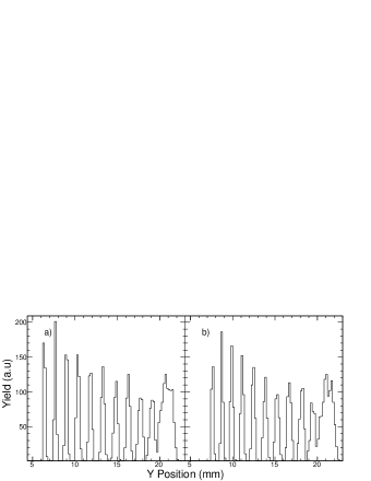
Using the measured magnetic field together with the SIMION-calculated electric field, the trajectory of electrons in the detector was simulated using the program SIMION [22]. To evaluate the spatial resolution, 100,000 electrons were generated on the masked, aluminized mylar foil and transported through the crossed magnetic and electric fields. An initial kinetic energy of 3eV was assumed for the electrons, consistent with the most probable initial electron energy for a similar experimental setup [29]. Although the initial kinetic energy distribution of ejected electrons extends out to 100 eV [29], it suffices to choose 3eV for the initial energy as the large bias potential applied to the electron emission foil overwhelms the initial kinetic energy chosen. To begin, we simulated the electron transport in a magnetic field with BY = 90G and BX = BZ = 0G. Electrons were assumed to be emitted within an initial angular cone with a half angle of 30∘[29] with one electron emitted for each incident particle. The simulated position spectrum on the MCP is depicted in Fig. 7a. Eleven peaks are observed with the peak at Y=21 mm significantly broader than the rest. The average spatial resolution of the ten narrower peaks observed in Fig. 7a is 572m FWHM. We also investigated the electron transport in the measured magnetic field for the same initial kinetic energy and angular distribution previously used. The simulated position spectrum for the measured magnetic field is depicted in Fig. 7b. The results of this magnetic field calculation are fairly similar to the previous case. The slight difference observed is that the broad peak at Y20 mm appears to be splitting into two peaks as evident in Fig. 7b. The average spatial resolution of the ten peaks with Y 20mm is 647m FWHM. The larger spatial resolution associated with the calculations utilizing the measured magnetic field indicate that variations in the field degrade the resolution. Efficiency was defined as the percentage of initial electrons originating from the slits that subsequently reach the multi-strip anode, which was determined to be 88 for both the measured and constant field simulations. We also investigated the position sensitivity in the Z-dimension using the same approach that was used in the Y-dimension. The position sensitivity in this dimension was determined to be 7mm.
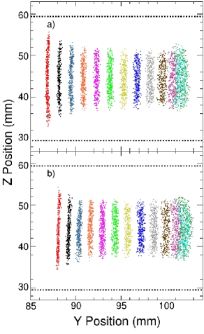
We investigated why the spectrum evident in Fig. 7b only exhibits 12 peaks. For the -particles incident on the 13 slits, the final YZ positions are shown in Fig. 8. In the case of BY = 90G and BX = BZ = 0G, presented in Fig. 8a, the image of the slits is observed as twelve vertical stripes. For reference, the area of the multi-strip anode is depicted by the dashed lines. As one moves to larger Y position, the width of each stripe increases resulting in poorer resolution. For the two slits at the largest value of Y, the slits are unresolved from each other. Thus the trend of resolution with position observed in Fig. 4 is reproduced. Two additional features can be noted in Fig. 8b. The vertical extent of the central stripes is somewhat smaller than that of the edge stripes indicating a contribution of focusing in the image by the field. In addition, the rightmost stripe exhibits a curvature not observed for the other stripes. Given the 7mm resolution in Z, by replacing the multi-strip anode with a cross-strip anode [5] a two-dimensional position measurement could be implemented.
6 Conclusion
An EB MCP detector with position-sensitivity in 1-dimension has been realized. Position-sensitivity was achieved by utilizing a MCP coupled to a multi-strip anode with delay line readout. Signals arriving at either end of the delay line were digitized by high speed digitizers and subsequently analyzed. To measure the position-sensitivity, a mask was inserted and the detector was exposed to -particles from an 241Am source. While the simplest analysis provided a measured spatial resolution of 520m FWHM, use of digital signal processing techniques along with use of signal selection criteria improved the spatial resolution to 413m. This measured resolution of 413m FWHM corresponds to an intrinsic resolution of 334m FWHM. To understand the measured resolution, the magnetic field was mapped, and the trajectories of ejected electrons were calculated using the program SIMION. For a constant magnetic field of BY = 90G and BX = BZ = 0G, simulations predict a spatial resolution of 572m FWHM. Use of the measured magnetic field results in a spatial resolution of 647 m FWHM. This approximate agreement of the simulation with the measured resolution suggests that the primary factors that influence the resolution are understood. The primary factor that dictates the measured resolution is the electron transport from the foil to the MCP. Although the present design provides good position sensitivity over a limited region in one-dimension, this initial development of a compact, high-rate position-sensitive EB detector is promising.
7 Acknowledgments
We gratefully acknowledge the technical support provided by the personnel in the Mechanical Instrument Services and Electronic Instrument Services (EIS) at the Department of Chemistry, Indiana University. In particular, we gratefully acknowledge A. Alexander of EIS for the design of the multi-strip anode and delay printed circuit boards. We thank Mr. Luis Morales (Notre Dame University) for providing additional magnetic field calculations which aided our understanding of the detector performance. This research is based upon work supported by the U.S. Department of Energy under Award Number FG02-88ER-40404, the National Nuclear Security Administration under Award Number DE-NA0002012, and the National Science Foundation under Grant Number 1342962.
References
- Wiza [1979] J. L. Wiza, Nucl. Inst. and Meth. Phys. Res. 162 (1979) 587.
- Fraser [1984] G. W. Fraser, Nucl. Inst. and Meth. Phys. Res. 221 (1984) 115.
- Sobottka and Williams. [1988] S. E. Sobottka, M. B. Williams, IEEE Trans. Nucl. Sci. 35 (1988) 348.
- Hong [2016] R. Hong, A. Leredde, Y. Bagdasarova, X. Fléchard, A. García, P. Müller, A. Knecht, E. Liénard, M. Kossin, M. G. Sternberg, H. E. Swanson, D. W. Zumwalt, Nucl. Inst. and Meth. A 835 (2016) 42.
- Siegmund et al. [2009] O. Siegmund, A. Tremsin, J. Vallerga, J. McPhate, Nucl. Inst. and Meth. A 610 (2009) 118.
- deSouza [2012] R. T. deSouza, Z. Q. Gosser, S. Hudan, Rev. Sci. Instrum. 83 (2012) 053305.
- deSouza [2015] R. T. deSouza, B. B. Wiggins, D. Siwal, IEEE Nucl. Sci. Symp. Med. Imaging Conf. (2015) 4018747.
- Lampton and Carlson [1979] M. Lampton, C. W. Carlson, Rev. Sci. Instrum. 50 (1979) 1093.
- Wiggins [2015] B. B. Wiggins, E. Richardson, D. Siwal, S. Hudan, R. T. deSouza, Rev. Sci. Instrum. 86 (2015) 083303.
- Siwal [2015] D. Siwal, B. B. Wiggins, R. T. deSouza, Nucl. Inst. and Meth. A 804 (2015) 144.
- Tremsin et al. [2011] A. S. Tremsin, J. B. McPhate, J. V. Vallerga, O. H. W. Siegmund, W. B. Feller, E. Lehmann, L. G. Butler, M. Dawson, Nucl. Inst. and Meth. A 652 (2011) 400.
- Shapira [2000] D. Shapira, T. A. Lewis, L. D. Hulett, Nucl. Instr. and Meth. A 454 (2000) 409.
- Matos [2012] M. Matoš, A. Estradé, H. Schatz, D. Bazin, M. Famiano, A. Gade, S. George, W. G. Lynch, Z. Meisel, M. Portillo, A. Rogers, D. Shapira, A. Stolz, M. Wallace, J. Yurkon, Nucl. Inst. and Meth. A 696 (2012) 171.
- Rogers [2015] A. M. Rogers, A. Sanetullaev, W. G. Lynch, M. B. Tsang, J. Lee, D. Bazin, D. Coupland, V. Henzl, D. Henzlova, M. Kilburn, M. S. Wallace, M. Youngs, F. Delaunay, M. Famiano, D. Shapira, K. L. Jones, K. T. Schmitt, Z. Y. Sun, Nucl. Inst. and Meth. A 795 (2015) 325.
- Bowman and Heffner [1978] J. D. Bowman, R. H. Heffner, Nucl. Instr. and Meth. Phys. Res. 148 (1978) 503.
- Kraus, Jr. et al. [1988] R. H. Kraus, Jr., D. J. Vieira, H. Wollnik, J. M. Wouters, Nucl. Inst. and Meth. A 264 (1988) 327.
- Odenweller [1982] T. Odenweller, H. Noll, K. Sapotta, R. E. Renfordt, R. Bass, Nucl. Inst. and Meth. Phys. Res. 198 (1982) 263.
- Steinbach et al. [2014] T. K. Steinbach, M. J. Rudolph, Z. Q. Gosser, K. Brown, B. Floyd, S. Hudan, R. T. deSouza, J. F. Liang, D. Shapira, M. Famiano, Nucl. Inst. and Meth. A 743 (2014) 5.
- Steinbach et al. [2014] T. K. Steinbach, J. Vadas, J. Schmidt, C. Haycraft, S. Hudan, R. T. deSouza, L. T. Baby, S. A. Kuvin, I. Wiedenhöver, A. S. Umar, V. E. Oberacker, Phys. Rev. C 90 (041603(R)) 5.
- Steinbach [2016] T. K. Steinbach, PhD thesis, Indiana University, 2016.
- Singh et al. [2017] Varinderjit Singh, J. Vadas, T. K. Steinbach, B. B. Wiggins, S. Hudan, R. T. deSouza, Zidu Lin, C. J. Horowitz, L. T. Baby, S. A. Kuvin, Vandana Tripathi, I. Wiedenhöver, Phys. Lett. B 765 (2017) 99.
- Mic [2017] SIMION, 2017. URL: http://www.simion.com.
- Mic [2017] Photonis USA, 2017. URL: http://www.photonis.com.
- Wiggins et al. [2017] B.B. Wiggins, to be published (2017).
- Mizogawa et al. [1997] T. Mizogawa, M. Sato, M. Yoshino, Y. Itoh, Y. Awaya, Nucl. Inst. and Meth. A 387 (1997) 395.
- Mag [2017] Master Magnetics Inc., 2017. URL: www.magnetsource.com.
- deSouza et al. [2011] R. T. deSouza, A. Alexander, K. Brown, B. Floyd, Z. Q. Gosser, S. Hudan, J. Poehlman, M. J. Rudolph, Nucl. Inst. and Meth. A 632 (2011) 133.
- Mic [2017] Alpha, 2017. URL: https://www.trifield.com/content/dc-gaussmeter-model-gm1-st/.
- Villette et al. [2000] J. Villette, M. Barat, P. Roncin, Rev. Sci. Instrum. 71 (2000) 2367.