Coulomb drag and counterflow Seebeck coefficient in bilayer-graphene double layers
Abstract
We have fabricated bilayer-graphene double layers separated by a thin (20 nm) boron nitride layer and performed Coulomb drag and counterflow thermoelectric transport measurements. The measured Coulomb drag resistivity is nearly three orders smaller in magnitude than the intralayer resistivities. The counterflow Seebeck coefficient is found to be well approximated by the difference between Seebeck coefficients of individual layers and exhibit a peak in the regime where two layers have opposite sign of charge carriers. The measured maximum counterflow power factor is 700 W/K2cm at room temperature, promising high power output per mass for lightweight thermoelectric applications. Our devices open a possibility for exploring the novel regime of thermoelectrics with tunable interactions between n-type and p-type channels based on graphene and other two-dimensional materials and their heterostructures.
keywords:
Graphene double layer , counterflow Seebeck coefficient , Coulomb drag , thermoelectrics1 Introduction
Graphene and boron nitride (BN) based heterostructures have attracted intense attention in recent years.[1, 2, 3, 4, 5] With the flake transfer technique[6, 7, 1, 2] that enables convenient stacking of a large variety of two-dimensional layered materials, high quality samples of graphene/BN/graphene (where the BN thickness can be as thin as down to 1 nm[8]) and other heterostructures have been fabricated to study the interlayer interactions. For example, strong Coulomb drag[8, 9, 10] and tunable metal-insulator transition[11] have been observed. Vertical field-effect transistor[12] and resonant tunneling[13, 14] using atomically thin barriers have been demonstrated, promising for applications in logic and high-frequency devices. The electron-hole symmetry allows each layer of graphene to be populated with electrons or holes using gates, which is usually difficult to achieve in traditional semiconductor quantum wells.[15] In the regime where one graphene layer is p-type while the other is n-type, the intriguing exciton condensation[16] has been predicted, though the predicted transition temperature spans a wide range.[17, 18, 19, 20, 21, 22, 23, 24, 25, 26] A recent proposal suggests that in bilayer-graphene (BLG) double layers, the transition temperature could be well above liquid helium temperatures at zero magnetic field.[25] This novel phase transition can be detected by performing counterflow transport (with equal magnitude and opposite direction of current in two layers), Coulomb drag and other measurements.[16, 27] An anomalous negative Coulomb drag is observed in BLG double layers,[9, 10] which is different from the drag in monolayer graphene double layers.[28, 8] Signatures of exciton superfluid have been recently observed in BLG in magnetic field with much higher transition temperature than that in double quantum wells.[29, 30, 16] In addition, thermoelectric transport is a powerful tool for studying not only the single particle transport,[31] but also strongly correlated systems[32, 33] and macroscopic quantum coherence[34, 35, 36] such as exciton condensation. Thermoelectric transport might also be relevant to understanding the drag measurements in BLG double layers.[9] Nevertheless, no counterflow thermoelectric transport measurements have been performed.
As another motivation for the current work, high efficiency thermoelectric modules have been pursued for decades to improve solid-state thermoelectric generators and Peltier refrigerators. Due to often conflicting parameters, producing such modules requires careful material and structural engineering.[37] High thermoelectric efficiency in low dimensional and nano-materials has been demonstrated, particularly for “electron-crystal-phonon-glass” systems that have high electrical conductivity and low thermal conductivity.[38, 37] These traditional approaches focus on engineering the properties of a given material to enhance the thermoelectric figure of merit , where is electrical conductivity, is Seebeck coefficient, is thermal conductivity and is temperature. Traditional thermoelectric units consist of two spatially separated and oppositely doped (p-type and n-type) semiconductor channel materials. The typical size of the channel materials and their separation are macroscopic, and their mutual interaction is negligible. In nanoscale thermoelectric devices, if the two channels are brought sufficiently close together, in principle the Coulomb interaction between the charge carriers in the two channels can become notable. It remains unknown how such interaction may affect the thermoelectric transport properties. Such a previous unexplored regime in thermoelectric devices may be studied in closely separated double layer systems, such as graphene/BN/graphene.
In this paper, Coulomb drag resistivity (which arises from the interlayer interaction) and counterflow Seebeck coefficient are measured in two BLG layers separated by a thin BN layer shown in Figure 1. The Coulomb drag resistivity and Seebeck coefficient in each BLG layer show the expected sign when the carrier type in each layer is changed. In our current devices, the counterflow Seebeck coefficient can be well approximated by the sum of Seebeck coefficients from the individual layers, suggesting that the effect of the interlayer interaction on the counterflow thermoelectric transport is negligibly small (although the interlayer interaction is sufficient to give a measurable Coulomb drag signal). The magnitude of counterflow Seebeck coefficient and the calculated counterflow power factor increase with temperature. We provide a quantitative analysis about the thermoelectric performance in the counterflow regime. The maximum power factor at room temperature can be 700 W/K2cm, exceeding that of the good thermoelectric material Bi2Te3 at least by a factor of 5.[39] Such a high power factor could be useful in thermoelectric applications, even though value is small due to high thermal conductivity of graphene. The possible impact of Coulomb drag on the counterflow Seebeck coefficient, though small in our samples, can be enhanced in devices with smaller separation between the two channels and could open new possibilities in developing high thermoelectric materials and structures.
2 Methods
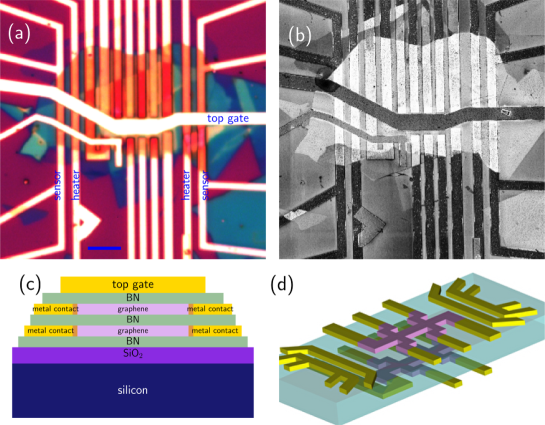
The measured graphene device in Figure 1a-b consists of two BLG layers separated by a thin BN layer (20 nm thick). They have isolated metal contacts, as shown by the schematics in Figure 1c-d. The bilayer nature of graphene is confirmed by Raman spectroscopy and quantum Hall measurement. This layered structure is sitting on a local BN dielectric on SiO2/silicon substrate and is covered by the top gate BN dielectric and metal. To fabricate the sample, the bottom BN layer is exfoliated onto the SiO2 (300 nm)/silicon substrate. The other graphene and BN layers are subsequently transfered using a home-built flake transfer stage with an alignment precision of few micrometers. We employ the flake transfer recipe[2] based on the sacrificial poly(methyl methacrylate) (PMMA) film coated on supporting polyvinyl alcohol (PVA) layer. After transferring each graphene layer, the device is annealed in H2(5 %)/Ar(95 %) at ambient pressure to remove the residual polymers. However PMMA residuals cannot be completely eliminated[40] and exist at the interfaces of graphene and BN. They can still slightly shift the charge neutral point and induce intralayer carrier scatterings where the interlayer scattering from polymer residual may be weak due to large thickness (20 nm thick) of the spacer BN layer. Oxygen plasma etching then defines the Hall bar configuration, followed by electron beam lithography and metalization (10 nm Ti and 70 nm Au). The metal lines for the heater and temperature sensor are fabricated together with the metal contacts for the top graphene layer. The device is then covered by the top BN dielectric followed by the top gate metal deposition. The device is finally bonded onto a chip carrier and measured in cryostats. Except the study of temperature dependence, all the other measurements are carried out at room temperature.
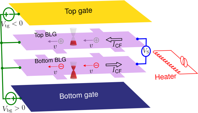
The electrical connection to measure the counterflow Seebeck coefficient is shown in Figure 2 where the counterflow Seebeck coefficient is specifically determined from the voltage measured between two layers at the right end while they are connected at the left. The lateral temperature difference () of 1 K[41] is established between two ends in each graphene layer. The top and bottom gate voltages and can control the carrier densities of the corresponding graphene layers, e.g., the top layer of p-type and the bottom layer of n-type here are indicated by the red filling of the parabolic band structures and the charge symbols and .
A low frequency alternating (AC) heating current of a few milliampere in amplitude is applied across the heater line and the counterflow Seebeck voltage (voltage drop from the top to bottom layer measured at the right ends) is then detected using a lock-in amplifier at the second harmonic (with 90 degree phase shift). The heater and temperature sensors are calibrated[42] to calculate the established (RMS) temperature difference [41] and convert the Seebeck voltage to Seebeck coefficient . The sign of is negative when the top and bottom graphene layers are p- and n-type respectively. During measuring , the resistances of both graphene layers are simultaneously measured using another two lock-in amplifiers at different lock-in frequencies. The frequencies for the three lock-in amplifiers are varied to ensure that the measured and resistances are insensitive to such variations, indicating independent thermoelectric and resistance response signals in each graphene layer.
3 Results
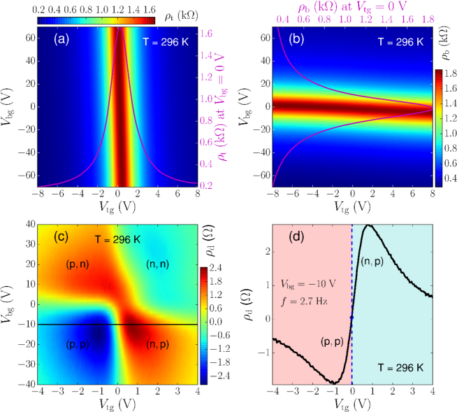
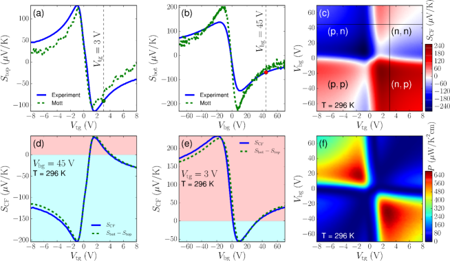
The tunneling resistance between two graphene layers is measured to be larger than 10 G, an indication of good electrical isolation between them. The color maps of intralayer resistivities and as functions of and for the top and bottom BLG are shown in Figure 3a and b respectively. The solid purple line in Figure 3a[b] is (plotted on the right axis) vs. [ (plotted on the top axis) vs. ] when []. It is obvious that the resistivity of the top [bottom] BLG layer cannot be effectively tuned by the bottom [top] gate voltage due to the strong screening by the bottom [top] BLG layer. The charge neutral point for the top [bottom] BLG layer slightly decreases as [] increases, due to the incomplete screening from the other graphene layer. The charge neutral points for both graphene layers are very close to zero gate voltage, since both graphene layers are sandwiched between two BN layers, resulting in reduced charge doping of the BLG layers.
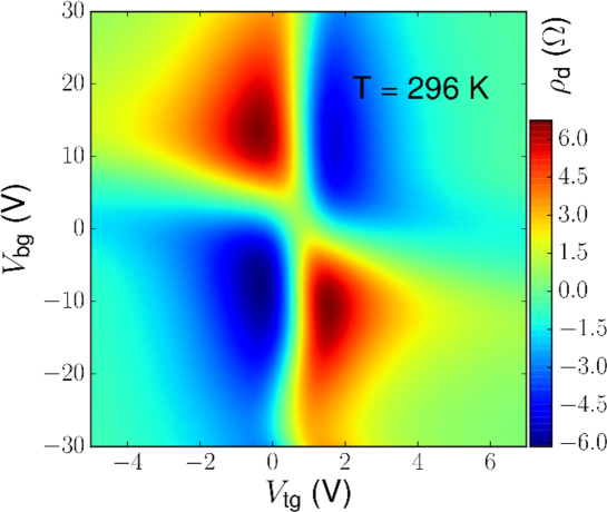
The color map of Coulomb drag resistivity vs. and is shown in Figure 3c, where the current is applied on the drive layer while the voltage is measured on the drag layer and is the ratio of the length along which is applied to the width of the graphene channel. The sign of is defined to be positive when has the same sign as the voltage drop in the drive layer when the drag layer has zero current. Various procedures (e.g., swapping the drag and drive layers, changing the grounding positions and varying the lock-in frequencies) are carried out to ensure the physical Coulomb drag signal is detected.[43] The Coulomb drag resistivity is measured at a low frequency of . The out-of-phase component of is at least one order of magnitude smaller than the in-phase component except around Dirac point where is close to zero. The solid line in Figure 3d is corresponding to the horizontal cut in Figure 3c at . The labels (x,y) in Figure 3c and d where x and y can be either n or p indicate that the charge carriers of the top BLG is of x-type while that of the bottom BLG is of y-type. Though the shape of the color map is not symmetrical (probably due to charge inhomogeneity), the sign of is correct, i.e, positive for opposite type of charge carriers in both BLG layers (xy) and negative for same type of charge carriers (xy). Note that the regions of positive located at the top left and bottom right quadrants are connected across the charge neutral point in both BLG layers, similar to the measurement of Coulomb drag between two single layer graphene (SLG) layers in Ref.[8]. For another sample of BLG double layers, the color map of Coulomb drag resistivity (see Figure S2 in the supplementary material) exhibits different behavior around the charge neutral point in both BLG layers but similar to another reported result for SLG double layers.[28] The color map of at temperature of 240 K and 200 K can be found in Figure S1 in the supplementary material. Recent measurements of Coulomb drag in BLG double layers show anomalous negative drag when the carriers in both layers are of the same type at temperatures below 200 K[10] and 10 K[9]. In our sample no such negative drag is observed for temperatures above 200 K. The drag resistivity is too small to allow reliable measurement of Coulomb drag signals.
The blue solid lines in Figure 4a[b] are the measured Seebeck coefficient of the top [bottom] BLG layer tuned by the top [bottom] gate voltage while the bottom [top] BLG layer is electrically floating. The green dashed lines are calculated from the Mott formula , where is the elementary charge, is the Boltzmann constant, is the gate voltage, is the intralayer resistivity, and is the Fermi level.[44] The vs. relation can be obtained by evaluating the energy dispersion ( for conduction band and for valence band) of BLG at the Fermi wave vector , where the Fermi velocity is m/s, eV, is the gate capacitance and is the gate voltage at the charge neutral point.[45] Note that the wiggles in the green dashed lines are due to the numerical computation of from the solid purple lines in Figure 3a and b.
The color map of counterflow Seebeck coefficient () vs. and at room temperature is shown in Figure 4c (temperature dependence of can be found in Figure S3 in the supplementary material). Four quadrants of this color map are separated by white areas near zero gate voltages. Large magnitude of negative [positive] appears in the top left [bottom right] quadrant when the top and bottom graphene layers are p- and n-type [n- and p-type] respectively. In this regime where two graphene layers have different carrier types, we found that the magnitude of is simply the sum of the magnitude of Seebeck coefficient in each individual layer. We do not find any noticeable interlayer interaction effects on due to the weak Coulomb drag in our samples ( is nearly three orders of magnitude smaller than or ). The magnitude of in the other two quadrants is smaller or even close to zero since the signs of Seebeck coefficient in both layers are same and they tend to cancel each other. The above discussion can be represented by the formula which is demonstrated in Figure 4d-e. For example in Figure 4d, the solid blue line is from the horizontal cut in Figure 4c while the dashed green line is calculated from where is the constant value taken at the red point in Figure 4b for and is the solid blue curve in Figure 4a. These two lines are close to each other, validating the above formula. The small discrepancy may come from the incomplete gating screening of BLG layers, resulting in small variation of the carrier density of the top [bottom] BLG when [] is changed and [] is fixed. The horizontal lines of zero in Figure 4d-e separate them into red (positive ) and cyan (negative ) areas. Note that the lines of vs. gate voltage cross zero twice, which is not possible for an isolated and homogeneous single layer of BLG. This explains that the top right and bottom left quadrants in Figure 4c are composed of regions with different sign of and the boundaries of white line segments with zero .
The power factor in the counterflow thermoelectric transport regime is defined as , where the BLG thickness (=0.67 nm) is introduced to allow convenient comparison of our measured results with the other experiments and calculations. Its color map is shown in Figure 4f. Note that the gate voltages corresponding to the maximum of are different from that of the magnitude of since the BLG resistivity is strongly dependent on the gate voltages. Here the extrinsic resistance mainly from the metal-graphene contacts is ignored, because it is material and process dependent and can be one order smaller than the graphene resistances after special contact treatment.[46] The maximum power factor is 700 W/K2cm. A very recent work has obtained similar power factor in graphene/BN devices.[47]
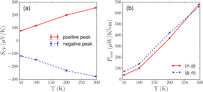
The positive and negative peak values of vs. temperature are shown in Figure 5a. The magnitudes of both peaks decrease with temperature. The maximum power factor in the two regimes of opposite carrier types for the two graphene layers (solid red [dashed blue] line for top layer of n-type [p-type] and bottom layer of p-type [n-type]) vs. temperature is shown in Figure 5b. These two lines show similar trend and manifest the symmetry between the two regimes. It is expected that will increase further as temperature increases above room temperature. Note that the peak values of and are both achieved in and regions, but the corresponding gate voltages are different.
4 Discussion
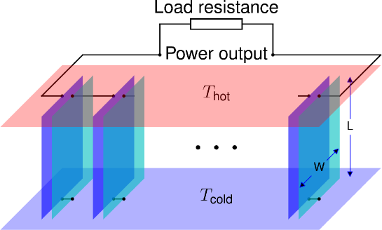
Although graphene has high Seebeck coefficient and electrical conductivity,[49, 50] hence high power factor, its is small due to its high thermal conductivity.[51, 52] While small materials are not good candidates for thermoelectric applications, significant effort has been devoted to enhancing the of graphene and related nanostructures,[53, 54, 55, 56, 57, 58, 59, 60, 61, 62, 63, 64, 65, 66, 67, 68, 69] usually by reducing the thermal conductivity with various methods. The high value of power factor is still promising in electricity generation at special circumstances, e.g., when space is constrained and high efficiency is not needed. The maximum output power for the thermoelectric module with serially connected (see Figure S5 in the supplementary material) units is at the impedance match[70] where the load resistance equals to the internal resistance () of the module, where is the ratio of the length (the length of graphene is measured along the direction of temperature gradient) to the width and 700 W/K2cm. The expression of indicates that the effective power factor () of serially connected units is proportional to , useful for building high output voltage thermoelectric modules. For large , the internal resistance of the module will be proportionally large and the power delivery capability will be limited when the load resistance is a constant. This issue can be resolved by reducing . The values of and can be optimally chosen for any specific load resistance and power requirement.
For K (e.g., the average temperature difference between the hot and cold spots in the modern CPUs), W for . Such serially connected thermopower generator has a thermal conductance of W/K for W/mK ( will be larger if the heat conduction channels through the insulating materials between graphene layers and the other supporting/gating materials are included), useful for applications of fast heat dissipation while generating electricity energy. Due to the low mass density of graphene, the power output per mass is as high as W/kg (the total graphene area is 20 m2) without including the mass of the insulating materials between graphene layers. It is still an extremely large number even when the mass of those insulating materials are included. For example, inserting a 3 nm thick of BN layer between graphene layers is good enough to avoid leakage between graphene layers. The mass density of BN is about 4.5 times larger than that of graphene, thus the power output per mass is reduced to W/kg. The mass of the other materials such as the gate metal (can be replaced by graphene or become not needed by doping graphene chemically for example) and interconnects (could be replaced by graphene) is not considered here. Such high power per mass makes graphene promising in light weight thermoelectric applications.[71]
The intralayer resistivities may be affected by the interlayer Coulomb drag,[72] which will affect the power factor. As seen from Figure 3c, the maximum magnitude of is about 2.5 , much smaller than the resistivity of each graphene layer. Therefore, such Coulomb drag effect can be neglected in the counterflow thermoelectric transport measured here. It may become important when is large, especially when it is close to the intralayer resistivities. Large Coulomb drag resistivity is an indication of strong interlayer interactions. It has been suggested that the formation of excitons composed of electron-hole pairs where the electrons and holes reside in different layers will possibly lead to high structures.[73, 74, 75]
5 Conclusion
In conclusion, Coulomb drag and counterflow thermoelectric transport measurements are performed in layered structures of BN/BLG/BN/BLG/BN. The magnitude of the counterflow Seebeck coefficient exhibits a peak in the regime where two graphene layers have opposite sign of charge carriers. The maximum power factor is about W/K2cm at room temperature. A quantitative analysis indicates that graphene can be useful for light weight thermoelectric systems. The counterflow Seebeck coefficient and power factor decrease with temperature from 300 K to 50 K. The measured interlayer Coulomb drag resistivity is small ( 3 ) compared to the intralayer resistivity, making negligible impact of Coulomb drag on the counterflow thermoelectric transport in the present structures. However, further reducing the separation between two BLG layers may shed light on the interplay between Coulomb drag and counterflow thermoelectric transport.
Acknowledgment
This work is supported by DARPA MESO (grant N66001-11-1-4107) and NIST MSE (grant 60NANB9D9175).
References
References
- [1] C. Dean, A. Young, I. Meric, C. Lee, L. Wang, S. Sorgenfrei, K. Watanabe, T. Taniguchi, P. Kim, K. Shepard, Boron nitride substrates for high-quality graphene electronics, Nature nanotechnology 5 (10) (2010) 722–726.
- [2] T. Taychatanapat, K. Watanabe, T. Taniguchi, P. Jarillo-Herrero, Quantum hall effect and landau-level crossing of dirac fermions in trilayer graphene, Nature Physics 7 (8) (2011) 621–625.
-
[3]
C. R. Dean, A. F. Young, P. Cadden-Zimansky, L. Wang, H. Ren, K. Watanabe,
T. Taniguchi, P. Kim, J. Hone, K. L. Shepard,
Multicomponent
fractional quantum hall effect in graphene, Nature Physics 7 (9) (2011)
693–696.
doi:10.1038/nphys2007.
URL http://www.nature.com/doifinder/10.1038/nphys2007 - [4] L. Britnell, R. V. Gorbachev, R. Jalil, B. D. Belle, F. Schedin, M. I. Katsnelson, L. Eaves, S. V. Morozov, A. S. Mayorov, N. M. Peres, Electron tunneling through ultrathin boron nitride crystalline barriers, Nano letters 12 (3) (2012) 1707–1710.
- [5] A. Geim, I. Grigorieva, Van der waals heterostructures, Nature 499 (7459) (2013) 419–425.
-
[6]
L. Jiao, B. Fan, X. Xian, Z. Wu, J. Zhang, Z. Liu,
Creation of
nanostructures with poly(methyl methacrylate)-mediated nanotransfer
printing, Journal of the American Chemical Society 130 (38) (2008)
12612–12613.
doi:10.1021/ja805070b.
URL http://pubs.acs.org/doi/abs/10.1021/ja805070b -
[7]
L. Jiao, X. Xian, Z. Wu, J. Zhang, Z. Liu,
Selective positioning
and integration of individual single-walled carbon nanotubes, Nano Letters
9 (1) (2009) 205–209.
doi:10.1021/nl802779t.
URL http://pubs.acs.org/doi/abs/10.1021/nl802779t - [8] R. Gorbachev, A. Geim, M. Katsnelson, K. Novoselov, T. Tudorovskiy, I. Grigorieva, A. MacDonald, S. Morozov, K. Watanabe, T. Taniguchi, Strong coulomb drag and broken symmetry in double-layer graphene, Nature physics 8 (12) (2012) 896–901.
- [9] K. Lee, J. Xue, D. C. Dillen, K. Watanabe, T. Taniguchi, E. Tutuc, Giant frictional drag in double bilayer graphene heterostructures, Physical Review Letters 117 (2016) 046803.
- [10] J. Li, T. Taniguchi, K. Watanabe, J. Hone, A. Levchenko, C. Dean, Negative coulomb drag in double bilayer graphene, Physical Review Letters 117 (2016) 046802.
- [11] L. Ponomarenko, A. Geim, A. Zhukov, R. Jalil, S. Morozov, K. Novoselov, I. Grigorieva, E. Hill, V. Cheianov, V. FalKo, Tunable metal-insulator transition in double-layer graphene heterostructures, Nature Physics 7 (12) (2011) 958–961.
- [12] T. Georgiou, R. Jalil, B. D. Belle, L. Britnell, R. V. Gorbachev, S. V. Morozov, Y.-J. Kim, A. Gholinia, S. J. Haigh, O. Makarovsky, Vertical field-effect transistor based on graphene-ws2 heterostructures for flexible and transparent electronics, Nature nanotechnology 8 (2) (2013) 100–103.
- [13] L. Britnell, R. Gorbachev, A. Geim, L. Ponomarenko, A. Mishchenko, M. Greenaway, T. Fromhold, K. Novoselov, L. Eaves, Resonant tunnelling and negative differential conductance in graphene transistors, Nature communications 4 (2013) 1794.
- [14] A. Mishchenko, J. Tu, Y. Cao, R. Gorbachev, J. Wallbank, M. Greenaway, V. Morozov, S. Morozov, M. Zhu, S. Wong, F. Whiters, C. Woods, Y. Kim, K. Watanabe, T. Taniguchi, E. Vdovin, O. Makarovsky, T. Fromhold, V. Falko, A. Geim, K. Novoselov, Twist-controlled resonant tunnelling in graphene/boron nitride/graphene heterostructures, Nature nanotechnology 9 (10) (2014) 808–813.
- [15] M. J. Manfra, Molecular beam epitaxy of ultra-high-quality algaas/gaas heterostructures: Enabling physics in low-dimensional electronic systems, Annual Review of Condensed Matter Physics 5 (1) (2014) 347–373. doi:10.1146/annurev-conmatphys-031113-133905.
- [16] J. Eisenstein, A. MacDonald, Bose–einstein condensation of excitons in bilayer electron systems, Nature 432 (7018) (2004) 691–694.
- [17] H. Min, R. Bistritzer, J.-J. Su, A. MacDonald, Room-temperature superfluidity in graphene bilayers, Physical Review B 78 (12) (2008) 121401.
- [18] Y. E. Lozovik, A. Sokolik, Electron-hole pair condensation in a graphene bilayer, JETP letters 87 (1) (2008) 55–59.
- [19] M. Y. Kharitonov, K. B. Efetov, Electron screening and excitonic condensation in double-layer graphene systems, Physical Review B 78 (24) (2008) 241401.
- [20] C.-H. Zhang, Y. N. Joglekar, Excitonic condensation of massless fermions in graphene bilayers, Physical Review B 77 (23) (2008) 233405.
- [21] Y. E. Lozovik, S. Ogarkov, A. Sokolik, Condensation of electron-hole pairs in a two-layer graphene system: Correlation effects, Physical Review B 86 (4) (2012) 045429.
- [22] D. Abergel, R. Sensarma, S. D. Sarma, Density fluctuation effects on the exciton condensate in double-layer graphene, Physical Review B 86 (16) (2012) 161412.
- [23] I. Sodemann, D. Pesin, A. MacDonald, Interaction-enhanced coherence between two-dimensional dirac layers, Physical Review B 85 (19) (2012) 195136.
- [24] Y. F. Suprunenko, V. Cheianov, V. I. Fal’ko, Phases of the excitonic condensate in two-layer graphene, Physical review b 86 (15) (2012) 155405.
- [25] A. Perali, D. Neilson, A. R. Hamilton, High-temperature superfluidity in double-bilayer graphene, Physical Review Letters 110 (14) (2013) 146803.
- [26] D. Abergel, M. Rodriguez-Vega, E. Rossi, S. D. Sarma, Interlayer excitonic superfluidity in graphene, Physical Review B 88 (23) (2013) 235402.
- [27] D. Nandi, A. Finck, J. Eisenstein, L. Pfeiffer, K. West, Exciton condensation and perfect coulomb drag, Nature 488 (7412) (2012) 481–484.
- [28] S. Kim, E. Tutuc, Coulomb drag and magnetotransport in graphene double layers, Solid State Communications 152 (15) (2012) 1283–1288.
- [29] X. Liu, K. Watanabe, T. Taniguchi, B. I. Halperin, P. Kim, Quantum hall drag of exciton superfluid in graphene, arXiv preprint arXiv:1608.03726.
- [30] J. Li, T. Taniguchi, K. Watanabe, J. Hone, C. Dean, Excitonic superfluid phase in double bilayer graphene, arXiv preprint arXiv:1608.05846.
- [31] C. Goupil, W. Seifert, K. Zabrocki, E. Müller, G. J. Snyder, Thermodynamics of thermoelectric phenomena and applications, Entropy 13 (8) (2011) 1481–1517.
- [32] D. M. Rowe, Thermoelectrics handbook: macro to nano, CRC press, 2005.
- [33] S. Lin, P. Tong, B. Wang, J. Lin, Y. Huang, Y. Sun, Good thermoelectric performance in strongly correlated system sncco3 with antiperovskite structure, Inorganic chemistry 53 (7) (2014) 3709–3715.
- [34] J. Clarke, S. Freake, Superconducting fountain effect, Physical Review Letters 29 (9) (1972) 588.
- [35] T. Karpiuk, B. Grémaud, C. Miniatura, M. Gajda, Superfluid fountain effect in a bose-einstein condensate, Physical Review A 86 (3) (2012) 033619.
- [36] A. Rançon, C. Chin, K. Levin, Bosonic thermoelectric transport and breakdown of universality, New Journal of Physics 16 (11) (2014) 113072.
- [37] G. J. Snyder, E. S. Toberer, Complex thermoelectric materials, Nature materials 7 (2) (2008) 105–114.
- [38] M. S. Dresselhaus, G. Chen, M. Y. Tang, R. Yang, H. Lee, D. Wang, Z. Ren, J.-P. Fleurial, P. Gogna, New directions for low-dimensional thermoelectric materials, Advanced Materials 19 (8) (2007) 1043–1053.
- [39] S. V. Ovsyannikov, V. V. Shchennikov, G. V. Vorontsov, A. Y. Manakov, A. Y. Likhacheva, V. A. Kulbachinskii, Giant improvement of thermoelectric power factor of bi 2 te 3 under pressure, Journal of Applied Physics 104 (5) (2008) 053713–053713.
- [40] Y.-C. Lin, C.-C. Lu, C.-H. Yeh, C. Jin, K. Suenaga, P.-W. Chiu, Graphene annealing: how clean can it be?, Nano letters 12 (1) (2011) 414–419.
- [41] Here 1 K is the RMS value of the temperature difference that is oscillating with a frequency of when an AC current with frequency is applied to the heater. is extracted from the measured voltages with 90∘ phase shift on the sensors.
-
[42]
J. P. Small, K. M. Perez, P. Kim,
Modulation of
thermoelectric power of individual carbon nanotubes, Phys. Rev. Lett. 91
(2003) 256801.
doi:10.1103/PhysRevLett.91.256801.
URL http://link.aps.org/doi/10.1103/PhysRevLett.91.256801 - [43] K. Das Gupta, A. Croxall, J. Waldie, C. Nicoll, H. Beere, I. Farrer, D. Ritchie, M. Pepper, Experimental progress towards probing the ground state of an electron-hole bilayer by low-temperature transport, Advances in Condensed Matter Physics 2011.
- [44] S.-G. Nam, D.-K. Ki, H.-J. Lee, Thermoelectric transport of massive dirac fermions in bilayer graphene, Physical Review B 82 (24) (2010) 245416.
- [45] E. McCann, V. I. Fal’ko, Landau-level degeneray and quantum hall effect in a graphite bilayer, Physical Review Letters 96 (8) 086805.
- [46] W. S. Leong, H. Gong, J. T. Thong, Low-contact-resistance graphene devices with nickel-etched-graphene contacts, ACS nano 8 (1) (2013) 994–1001.
- [47] J. Duan, X. Wang, X. Lai, G. Li, K. Watanabe, T. Taniguchi, M. Zebarjadi, E. Y. Andrei, High thermoelectricpower factor in graphene/hbn devices, Proceedings of the National Academy of Sciences 113 (50) (2016) 14272–14276.
- [48] BIPM, IEC, IFCC, ILAC, IUPAC, IUPAP, ISO, OIML, Evaluation of measurement data – guide for expression of uncertainty in measurement, Tech. rep., Joint Committee for Guides in Metrology (2008).
- [49] J.-H. Chen, C. Jang, S. Xiao, M. Ishigami, M. S. Fuhrer, Intrinsic and extrinsic performance limits of graphene devices on sio2, Nature nanotechnology 3 (4) (2008) 206–209.
- [50] N. Sankeshwar, S. Kubakaddi, B. Mulimani, Thermoelectric power in graphene, Intech 9 (2013) 1–56.
- [51] A. A. Balandin, Thermal properties of graphene and nanostructured carbon materials, Nature materials 10 (8) (2011) 569–581.
- [52] E. Pop, V. Varshney, A. K. Roy, Thermal properties of graphene: Fundamentals and applications, Mrs Bulletin 37 (12) (2012) 1273–1281.
- [53] H. Sevinçli, G. Cuniberti, Enhanced thermoelectric figure of merit in edge-disordered zigzag graphene nanoribbons, Physical Review B 81 (11) (2010) 113401.
- [54] Y. Chen, T. Jayasekera, A. Calzolari, K. Kim, M. B. Nardelli, Thermoelectric properties of graphene nanoribbons, junctions and superlattices, Journal of Physics: Condensed Matter 22 (37) (2010) 372202.
-
[55]
F. Mazzamuto, V. Hung Nguyen, Y. Apertet, C. Caër, C. Chassat,
J. Saint-Martin, P. Dollfus,
Enhanced
thermoelectric properties in graphene nanoribbons by resonant tunneling of
electrons, Phys. Rev. B 83 (2011) 235426.
doi:10.1103/PhysRevB.83.235426.
URL http://link.aps.org/doi/10.1103/PhysRevB.83.235426 - [56] W. Huang, J.-S. Wang, G. Liang, Theoretical study on thermoelectric properties of kinked graphene nanoribbons, Physical Review B 84 (4) (2011) 045410.
- [57] T. Gunst, T. Markussen, A.-P. Jauho, M. Brandbyge, Thermoelectric properties of finite graphene antidot lattices, Physical Review B 84 (15) (2011) 155449.
- [58] L. Liang, E. Cruz-Silva, E. C. Girão, V. Meunier, Enhanced thermoelectric figure of merit in assembled graphene nanoribbons, Physical Review B 86 (11) (2012) 115438.
- [59] H. Zheng, H. Liu, X. Tan, H. Lv, L. Pan, J. Shi, X. Tang, Enhanced thermoelectric performance of graphene nanoribbons, Applied Physics Letters 100 (9) (2012) 093104.
- [60] Z.-X. Xie, L.-M. Tang, C.-N. Pan, K.-M. Li, K.-Q. Chen, W. Duan, Enhancement of thermoelectric properties in graphene nanoribbons modulated with stub structures, Applied Physics Letters 100 (7) (2012) 073105.
- [61] G. Kliros, P. Divari, Thermoelectric properties of gated graphene ribbons in the ballistic regime, Superlattices and Microstructures 52 (2) (2012) 221–233.
-
[62]
K. Yang, Y. Chen, R. D’Agosta, Y. Xie, J. Zhong, A. Rubio,
Enhanced
thermoelectric properties in hybrid graphene/boron nitride nanoribbons,
Phys. Rev. B 86 (2012) 045425.
doi:10.1103/PhysRevB.86.045425.
URL http://link.aps.org/doi/10.1103/PhysRevB.86.045425 - [63] H. Karamitaheri, N. Neophytou, M. Pourfath, R. Faez, H. Kosina, Engineering enhanced thermoelectric properties in zigzag graphene nanoribbons, Journal of Applied Physics 111 (5) (2012) 054501.
- [64] P.-H. Chang, B. K. Nikolić, Edge currents and nanopore arrays in zigzag and chiral graphene nanoribbons as a route toward high-z t thermoelectrics, Physical Review B 86 (4) (2012) 041406.
- [65] C.-N. Pan, Z.-X. Xie, L.-M. Tang, K.-Q. Chen, Ballistic thermoelectric properties in graphene-nanoribbon-based heterojunctions, Applied Physics Letters 101 (10) (2012) 103115.
- [66] H. Sevinçli, C. Sevik, T. Çağın, G. Cuniberti, A bottom-up route to enhance thermoelectric figures of merit in graphene nanoribbons, Scientific reports 3.
- [67] P. S. E. Yeo, M. B. Sullivan, K. P. Loh, C. K. Gan, First-principles study of the thermoelectric properties of strained graphene nanoribbons, Journal of Materials Chemistry A 1 (36) (2013) 10762–10767.
- [68] B. Feng, J. Xie, G. Cao, T. Zhu, X. Zhao, Enhanced thermoelectric properties of p-type cosb 3/graphene nanocomposite, Journal of Materials Chemistry A 1 (42) (2013) 13111–13119.
- [69] H. Chen, C. Yang, H. Liu, G. Zhang, D. Wan, F. Huang, Thermoelectric properties of cuinte 2/graphene composites, CrystEngComm 15 (34) (2013) 6648–6651.
- [70] Y. Apertet, H. Querdane, C. Goupil, P. Lecoeur, Optimal working conditions for thermoelectric generators with realistic thermal coupling, Europhysics Letters 97 (2012) 28001.
- [71] K. Yazawa, A. Shakouri, Cost-efficiency trade-off and the design of thermoelectric power generators, Environmental science & technology 45 (17) (2011) 7548–7553.
- [72] E. Tutuc, M. Shayegan, D. Huse, Counterflow measurement in strongly correlated gaas hole bilayers: evidence for electron-hole pairing, Physical Review Letters 93 (3) (2004) 036802.
- [73] K. Wu, L. Rademaker, J. Zaanen, Bilayer excitons in two-dimensional nanostructures for greatly enhanced thermoelectric efficiency, Phys. Rev. Applied 2 (2014) 054013.
-
[74]
Y. Chen, Surface excitonic
thermoelectric devices, uS Patent App. 13/312,986 (Jun. 7 2012).
URL http://www.google.com/patents/US20120138115 - [75] J. Hu, D. B. Newell, Y. Chen, unpublished.
- [76] E. T. Jaynes, Probability theory: the logic of science, Cambridge University Press, 2003.
Supporting Information
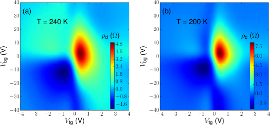
The color maps of Coulomb drag resistivity at T = 240 K and T = 200 K are shown in Figure S1a and b respectively. The data below 200 K is not collected due to small signal to noise ratio of the Coulomb drag signal. The measured data exhibits the anomalous behavior that the magnitude of the red peak of increases when the temperature is reduced. This is possibly due to the sample inhomogeneity.
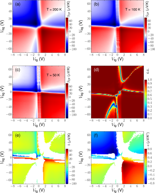
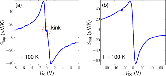
The color maps of at T = 200 K, 100K and 50 K are shown in Figure S3a-c. As the temperature decreases, decreases and the red area of positive increases for the top right and bottom left quadrants in the color maps. The positive and negative peaks of are slightly shifted closer to zero gate voltages and become more concentrated as the temperature is reduced. Many puddles of appear mainly around 0 V for temperatures 100 K and 50 K at which the Seebeck coefficient of the top BLG vs. exhibits kinks (see Figure S4) around the charge neutral point of top BLG, unlike that of the bottom BLG smoothly crosses zero. This could be due to the manifestation of the charge inhomogeneity in the top BLG layer at lower temperatures and possibly the small misalignment of the two BLG layers during sample fabrication, resulting in disturbed Seebeck coefficient of the top BLG layer around its charge neutral point. The color maps of the correlation coefficient (c.c., defined later) of vs. T and the intercept and the slope for the relation are shown in Figure S3d, e and f respectively. The blank area in Figure S3d and f corresponds to the gate voltages at which the c.c. in Figure S3d is less than 0.99. The magnitude of the intercept in Figure S3e is close to zero for the majority area of gate voltages away from the charge neutral point, indicating that is indeed linearly dependent on temperature.
The c.c. between two sets of data, e.g., {} and {} is defined as where and . The magnitude of c.c. measures the linearity between the two data sets: c.c. = 1 implies that the two sets are perfectly linearly dependent.[76]