Cavity QED with hybrid nanocircuits: from atomic-like physics to condensed matter phenomena
Abstract
Circuit QED techniques have been instrumental to manipulate and probe with exquisite sensitivity the quantum state of superconducting quantum bits coupled to microwave cavities. Recently, it has become possible to fabricate new devices where the superconducting quantum bits are replaced by hybrid mesoscopic circuits combining nanoconductors and metallic reservoirs. This mesoscopic QED provides a new experimental playground to study the light-matter interaction in electronic circuits. Here, we present the experimental state of the art of Mesoscopic QED and its theoretical description. A first class of experiments focuses on the artificial atom limit, where some quasiparticles are trapped in nanocircuit bound states. In this limit, the Circuit QED techniques can be used to manipulate and probe electronic degrees of freedom such as confined charges, spins, or Andreev pairs. A second class of experiments consists in using cavity photons to reveal the dynamics of electron tunneling between a nanoconductor and fermionic reservoirs. For instance, the Kondo effect, the charge relaxation caused by grounded metallic contacts, and the photo-emission caused by voltage-biased reservoirs have been studied. The tunnel coupling between nanoconductors and fermionic reservoirs also enable one to obtain split Cooper pairs, or Majorana bound states. Cavity photons represent a qualitatively new tool to study these exotic condensed matter states.
I Introduction
Since the 1980’s, the continuous progress of nanofabrication techniques has enabled the fabrication of a wide diversity of nanoelectronics devices which reveal the oddities of quantum mechanics when placed at low temperatures. The strong confinement of electrons in narrow conductors leads to a quantization of transport into a few transverse channels. This phenomenon has been observed for instance in quantum point contacts made in a two-dimensional electron gas in a semiconductorvan Wees: 1988 , or in break-junctions between metalsKrans:1993 , where the electric current can be carried by a very low number of transverse channels. Another major ingredient of nanoelectronics is the longitudinal confinement of electrons between two potential barriers along the transport pathKouwenhoven:1997 . This leads to the formation of quantum dots with a discrete energy spectrum, which are often seen as artificial atoms. The fabrication of quantum dot circuits has reached a very high level of control in two-dimensional electron gas structures, where small quasi-zero dimensional dots are contacted to large two-dimensional reservoirs through quantum point contactsShulman:2012 . Interesting alternatives are offered by self-assembled quantum dotsKlein:1997 , carbon nanotubesTans:1997 and semiconducting nanowiresDe Franceschi:2003 . To form a nanocircuit with these nanoconductors, one must contact them with metallic electrodes which can be made out of normal metals, ferromagnets or superconductors. Due to the versatility of nanofabrication techniques, many circuit configurations can be used, with for instance multiple metallic contacts, or superconducting flux loops. This leads to a large variety of configurations to study quantum transport and obtain new electronic functionalities. For instance, a quantum dot coupled to ferromagnetic contacts can show a ferromagnetic proximity effect which is interesting for the control of spin transportCottet:2006a or for local spin manipulationsCottet:2010 . Other intriguing example, the Cooper pair splitter enables the spatial separation of the two spin-entangled electrons from a Cooper pair into two different quantum dots, which could be an interesting resource for quantum informationRecher:2001 . Finally, semiconducting nanowires coupled to superconductors raise a strong interest in the context of the search for topological matter and Majorana bound statesLeijnse:2012 . In these three examples, the coupling between the nanoconductors and the superconducting or ferromagnetic reservoirs deeply modifies the electronic properties of the nanoconductors. The hybrid nature of nanoelectronics devices therefore appears as an essential feature.
The first nanoelectronics experiments where naturally based on dc transport measurements. However, it soon appeared that studying the response of nanocircuits to a microwave excitation was also very interesting. For instance, photo-assisted tunneling was observed in quantum dot circuits, either between a dot and a reservoirKouwenhoven or inside a double quantum dotOosterkamp . A microwave irradiation was used to investigate the Kondo physics in a quantum dot with normal metal reservoirsElzerman . Radio-frequency single electron transistorsSchoelkopf:1998 were used for the electrometry of quantum dots Fujisawa:2000 ; Cassidy:2007 ; Reilly:2007 . Wide-bandOta:2010 and resonantPetersson:2010 ; Chorley:2012 techniques were developed to measure the impedance of quantum dot circuits. Microwaves were finally used to perform coherent manipulations of single chargesHayashi:2003 or spinsKoppens:2006 ; Nowack:2007 .
A new impulse on the microwave operation of electric nanocircuits is now starting under the influence of Cavity and Circuit Quantum Electrodynamics (QED). These experiments study respectively atoms strongly coupled to high finesse superconducting mirror cavitiesRaimond: 2001 , or superconducting Josephson circuits strongly coupled to microwave resonatorsWallraff:2004 ; Paik:2011 . In both cases, one can study the interaction of light and matter at the most elementary level because the cavity can trap a controlled low number of photons with a high spectral purity. Furthermore, the atoms and Josephson circuits behave as effective two-level systems. By analogy with these experiments, the idea of combining quantum dot circuits and microwave cavities came out theoretically mainly with the motivation of using quantum dots as quantum bits for quantum information scienceImamoglu ; Burkard:2006 . In that context, quantum dot circuits are operated in a well confined regime, i.e. the tunnel junctions between the dots and reservoirs are very opaque in order to minimize possible decoherence due to these reservoirs, and the metallic reservoirs are grounded to prevent dc transport. Several strategies are possible to reach the strong coupling regime between a nanocircuit and cavity photons. In particular, one can use the chargebruhat:2017 ; Mi:2017 ; Stockklauser:2017 or spin degree of freedomViennot:2015 of a double quantum dot, or Andreev bound states on a narrow superconducting contactJanvier:2015 . This could offer new means to encode and manipulate quantum information in the context of the development of quantum computing and quantum communication.
Nevertheless, using nanocircuits coupled to microwave cavities to mimic atomic cavity QED or Circuit QED experiments is a bit restrictive since it evades quantum transport effects which occur in out-of equilibrium conditions, as well as strong correlations effects caused by highly transparent dot-metal contacts. Along this direction, it appears that the use of microwave cavities combined with hybrid nanocircuits enables experiments with no analogue in atomic Cavity QED or metallic Circuit QED. Indeed, cavity photons provide means to study quantum transport under a new perspective and with a very high sensitivity. For instance, they can give a direct access to the out-of-equilibrium state occupation of a double quantum dotViennot:2014a , reservoir-induced quantum charge relaxation in a single dotBruhat:2016a , or photo-assisted tunneling processesBruhat:2016a ; Stockklauser:2015 ; Liu:2014 ; Liu:2015a ; Liu:2015 . They can also represent a powerful tool to characterize exotic condensed matter states caused by the existence of the dot/reservoir interfaces, such as Kondo cloudsDesjardins:2017 , split Cooper pairsCottet:2012 ; Cottet:2014 , or Majorana bound statesTrif:2012 ; Schmidt:2013a ; Schmidt:2013b ; Cottet:2013 ; Dmytruk:2015 ; Dartiailh:2016 .
Following Ref.Childress:2004 , we will refer to experiments combining microwave cavities and electronic nanocircuits as Mesoscopic QED experiments because the metallic reservoirs in a nanocircuit are typically separated by a micronic distance (see for instance Fig.1c). The purpose of this short review is to introduce this recent but fast growing new field of research and give possible directions for its future developments. In section II, we describe the Mesoscopic QED architecture. In section III, we present a theoretical description of Mesoscopic QED devices, from the mesoscopic QED Hamiltonian to the semiclassical description of the cavity signals. In section IV, we review experiments performed so far in the artificial atom limit. In section V, we discuss Mesoscopic QED experiments beyond the artificial atom limit, i.e. when the tunneling dynamics between the nanoconductor and metallic reservoir leads to significant effects. Section VI presents conclusions and perspectives. In this review we use in most equations, and we will thus define many parameters as pulsations. We note e the absolute value of the electron charge ().
II Building a Mesoscopic QED experiment
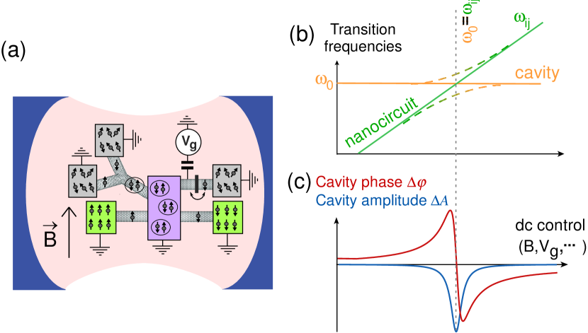
II.1 Embedding a hybrid nanocircuit in a microwave cavity
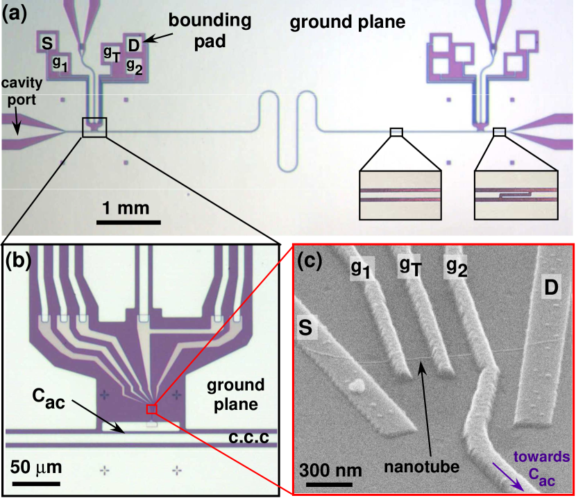
The combination of hybrid nanocircuits with coplanar microwave cavities pushes further the on-chip design initially introduced in the context of Circuit QED experiments to control and readout the state of a superconducting quantum bitWallraff:2004 . Many different types of nanoconductors have already been embedded in coplanar cavities, such as lateral quantum dots defined on a GaAs/AlGaAs heterostructuresFrey:2011 ; Toida:2012 or Si/SiGe heterostructuresSchmidt:2014 ; Mi:2016 , quasi-one dimensional conductors such as carbon nanotubesDelbecq:2011 ; Ranjan:2015 , InAs nanowiresPetersson:2012 ; Larsen:2015 ; Lange:2015 , or InSb nanowiresWang:2016 , but also graphene quantum dotsZhang:2014 and atomic contactsJanvier:2015 . Different types of metallic contacts can be used, such as normal metals, superconductors Bruhat:2016a and ferromagnets with collinearCottet:2006a or non-collinear magnetizationsCrisan: 2016 ; Viennot:2015 . Therefore, a large variety of geometries and situations can be studied. Figure 1 shows an example of Mesoscopic QED sample. Here, the hybrid nanocircuit is a double quantum dot fabricated out of a carbon nanotube on top of which source (S), drain (D), and top dc gates (, and ) have been evaporated (Fig.1c). The double dot is coupled capacitively to the cavity central conductor (c.c.c.), through the capacity , near a cavity electric field antinode (Fig.1b). The cavity central conductor is interrupted by on-chip capacitances such as the one visible in the right inset of Fig.1a. Openings are fabricated across the cavity ground plane to allow for an electric connection of the source, drain and gate electrodes of the double dot at bonding pads visible as squares in Fig.1a. These openings must be designed in order to preserve the cavity quality factor. To avoid spurious photon dissipation, it is also important to introduce as little conductors as possible close to the cavity. In experiments realized with semiconducting nanowires and first experiments realized with carbon nanotubes, numerous nanoconductors have been dispersed on the substrate during the fabrication process. Stamping techniquesWaissman:2013 are now used to deposit few carbon nanotube inside the cavityViennot::2014b , which leads to cavity quality factors Viennot:2015 ; Bruhat:2016a . In the case of nanostructures based on two-dimensional electron gases, the coupling to the whole electronic substrate seems more difficult to avoid. Among other technical progresses, one can mention the measurement of a double quantum dot in a cavity by using a Josephson parametric amplifier which considerably speeds up data acquisitionStehlik:2015 . Microwave-frequency resonators based on NbTiN nanowiresSamkharadze:2016 and SQUID arraysStockklauser:2017 have been recently developed in order to increase by a factor of 10 the cavity electric field in comparison with standard coplanar cavities based on Al or Nb metallic stripes. This can be used to increase the light/matter coupling. Other alternative cavity technologies compatible with nanocircuit architectures are being investigatedKopke:2015 ; Gotz:2016 ; Blien:2016 .
II.2 Tailoring the spectrum of a hybrid nanocircuit with fermionic reservoirs
One important specificity of circuit QED experiments performed with superconducting quantum bits, in comparison with atomic cavity QED experiments, is that the spectrum of a superconducting quantum bit is not set by nature like the spectrum of an atom, but it can be designed at the nanolithography stage by choosing the circuit geometry and the value of the capacitive and Josephson elements. This spectrum can also be tuned during the experiment by using gate voltages or magnetic fluxes. This represents a significant advantage for performing various tasks such as the selective microwave control of different quantum bits in an experiment. In Mesoscopic QED, the use of fermionic reservoirs offers other resources to tailor the spectrum of a nanocircuit. One must find configurations where the nanocircuit displays energy scales comparable with the cavity frequency. In this section, we discuss different possibilities to do so.
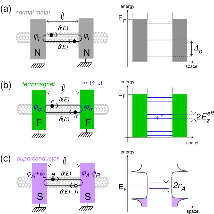
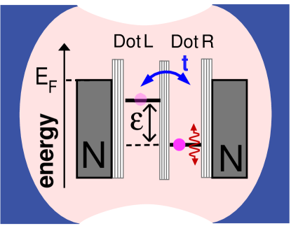
For simplicity, we first consider the case where two normal metal reservoirs delimit a single quantum dot with length inside a single channel nanoconductor (Fig.2a). In a non-interacting scattering picture, the phase shift acquired by an electron which crosses once the dot is , where , and are the Fermi energy, wavevector and velocity inside the nanoconductor and is the electron energy treated at first order. The electron is reflected on the normal metal contacts with a spin-independent reflection phase , so that the dot orbital energies are given by the resonant condition , with (see Fig.2a). This corresponds to an orbital level spacing
| (1) |
which is typically in the THz range, whereas the cavity frequency is typically of the order of . Resonant effects between microwave cavity photons and this local orbital degree of freedom are therefore impossible. However, there exists other configurations more favorable to reach the resonant regime as we will see below.
Ferromagnetic materials are widely used to control spin transport in industrial spintronics devicesFert:2008 . They also represent a promising resource for coherent nanocircuits. If a quantum dot is delimited by ferromagnetic contacts, the reflection phases on its boundaries can become spin-dependent, because the Stoner exchange fields inside the ferromagnets provide a spin dependent confinement potential for electrons in the dotCottet:2006b (see Fig.2b). Hence, an effective Zeeman splitting
| (2) |
occurs inside the dot. The factor in the above equation occurs because is an interference effect between the two contacts, given by the resonance condition , for spin . Due to this factor, can reach values of the order of for small dots with ()Cottet:2006a . In principle, this value is larger than stray fields from standard ferromagnets, which are independent of and reach typically a few . Furthermore, the effective field of Eq.(2) presents the advantage of being local, which can be useful for building complex devices.
Another interesting possibility to modify the spectrum of a nanocircuit is to use superconducting contacts which produce the Andreev reflection of an electron quasiparticle into a hole quasiparticle and vice versa (see Fig.2c). For simplicity, we will consider the case where only the value of the superconducting gap changes at the superconductor/nanoconductor interface, from to 0, in a single channel model. In this case, the resonant condition between the two contacts is , with the Andreev phase and the phase of the superconducting order parameter in the left(right) contact. Therefore, in the limit , the interferences between electron and holes lead to the creation of an Andreev doublet at energies with
| (3) |
One has for instance for aluminium electrodes. Hence, the scale can become very close to the cavity frequency if the superconductor/quantum dot/superconductor junction is inserted inside a flux biased superconducting loop in order to obtain . Note that the Andreev doublet discussed above has a two-fold degeneracy, since it can be produced by spin electrons and spin holes as well as spin electrons and spin holes. Such a degeneracy has to be taken into account for predicting the microwave response of superconducting nanostructures, as we will see in section IV.4. In summary, ferromagnetic and superconducting contacts offer interesting possibilities to make the spin or the electron/hole energy scales of a single quantum dot comparable to the cavity frequency. In contrast, the local charge degree of freedom associated to the scale is expected to be off resonant. Note that there can be a local orbital degeneracy related to the atomic structure of the nanoconductor, such as the K/K’ degree of freedom in a carbon nanotube. Effects related to this type of degree of freedom will be evoked in section 4.3.3.
Above, we have discussed exclusively the spectrum of a single quantum dot delimited by fermionic contacts, in order to find intradot degrees of freedom which could be coupled resonantly to the cavity. However, we will see in the next sections that non-local charge degrees of freedom associated to tunneling processes also play a major role in Mesoscopic QED. First, there can be tunneling between two dots separated by a tunnel barrier with a hopping constant (see Fig.15). This strongly affects the spectrum of a double quantum dot, where bonding and antibonding states appear. In practice, can be obtained with many different types of nanoconductors. Second, electrons can tunnel between a quantum dot and a metallic reservoir with a tunnel rate which can also be of the order of . These two types of resonances can lead to interesting effects, as we will see below.
III Theory of light-matter interaction in mesoscopic QED devices
III.1 The Mesoscopic QED Hamiltonian
III.1.1 Comparison between the different types of cavity QED experiments
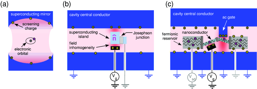
It is instructive to make a comparison of the physical ingredients involved in Cavity, Circuit and Mesoscopic QED to identify the specificities of the light-nanocircuit interaction. Cavity QED focuses on the interactions between electrons in the atomic orbitals of a flying atom and the photons trapped inside a superconducting mirror cavity (see Fig.3a). In these experiments, the effect of the cavity magnetic field on the atom can be disregarded for weak microwave amplitudesCohen-Tannoudji:book1 . In most situations, one can consider that the cavity electric field is constant on the scale of the atom because the atom is very small in comparison with the cavity. In this case, the light-matter interaction can be expressed quantum mechanically as with the quantized cavity electric field and the dipole associated to the atomic charges at position . Note that this charge distribution includes electrons but also the ions of the atom nucleus. However, the explicit description of these ions essentially grants the electroneutrality condition which simplifies calculations. Cavity QED mainly focuses on electronic transitions between the atomic orbitals, induced by the cavity electric field.
In circuit QED, the concept of orbital degree of freedom is not relevant anymore because only macroscopic collective degrees of freedom matter, due to the rigidity of the superconducting phase. For instance, in a Cooper pair box, which is a small superconducting island coupled to a superconducting reservoir through a Josephson junction, only the total excess number of electrons on the island matters (see Fig.3b). A second important difference with atomic Cavity QED is that the cavity field cannot be considered as homogeneous on the scale of the superconducting quantum bit. Indeed, its spatial profile is strongly modified by the presence of the superconducting elements which tend to expel it. Figure 3b illustrates this situation in the case of a Cooper pair box embedded in a coplanar microwave cavity. The cavity electric field concentrates in capacitive areas between neighboring metallic elements, as represented by the darker pink areas. This capacitive coupling scheme is often described with a lumped element circuit model which discretizes the device into nodes with uniform photonic potential and superconducting phase, connected by capacitors, inductors or Josephson junctions. In the simplest picture, the cavity is modeled as a distributed (L,C) line, and the superconducting island in Fig.3b corresponds to a single node contacted through capacitors and a Josephson junction to the rest of the circuit (see Figure 2 of Ref.Blais:2004 ). The cavity electric field shifts the island potential due to the presence of the capacitive coupling between the dot island and the cavity central conductor. Recently, more sophisticated lumped element circuit models have been introduced for a more realistic description of circuit QED devicesNigg:2012 ; Solgun:2014 . Note that Josephson circuits with superconducting loops may equally couple to the cavity magnetic field (not represented in Fig.3b).
Mesoscopic QED represents an intermediate situation between Cavity and Circuit QED (see Fig.3c). Indeed, due to the existence of small confined nanoconductor areas (like for instance quantum dots), there exists discrete electronic orbital levels which recall the atomic orbitals of Cavity QED. However, the cavity field is strongly inhomogeneous on the scale of the nanocircuit, which rather recalls circuit QED. For instance, one can use ac gates often connected directly (see Fig.3c) or sometimes capacitively (see Fig.1) to the cavity central conductor to reinforce locally the coupling between the cavity electric field and the electrons in one small part of the nanocircuit. The area between the ac gate and the nanoconductor in Fig.3c concentrates the electric field, as represented by the darker pink shade. This provides a capacitive coupling between the cavity central conductor and the nanoconductor. Field screening effects represent another source of field inhomogeneity. First, the cavity fields are confined between the superconducting cavity conductors, represented in blue in Fig.3c. This effect naturally goes together with a screening of the fields inside the cavity conductors. Second, the fermionic reservoirs in the nanocircuit can screen at least partially the cavity fields. These screening effects are due to electronic plasmonic modes, which are only implicitly taken into account in the usual descriptions of Circuit QED, through current conservation. In mesoscopic QED, it is not a priori obvious to take into account plasmonic modes because one must take into account that fermionic reservoirs host simultaneously plasmonic modes and fermionic quasiparticle modes which cause quantum transport effects in the nanocircuit. These quasiparticle modes are coupled to the localized discrete electronic orbitals inside the nanoconductors through tunnel junctions. Tunneling is also at the heart of the Josephson coupling in superconducting circuits. However, tunneling from a normal metal reservoir involves the numerous quasiparticle modes in a reservoir on top of the nanoconductor levels. Therefore, the study of Mesoscopic QED devices requires a description which combines physical ingredients from both Cavity and Circuit QED. In the following, we will follow the approach proposed by Ref.Cottet:2015 .
III.1.2 Effective decomposition of a Mesoscopic QED device
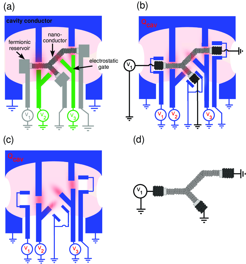
In order to take into account both quasiparticle tunneling and plasmonic screening in a minimal way, one can assume that the plasmonic screening charges on the cavity conductors or fermionic reservoirs have a frequency which is much higher than all the other relevant frequencies in the device. In particular, we assume that the plasmonic frequency is much higher than the tunnel rate between a reservoir and a nanoconductor, or than the tunnel hopping constant between two dots. Under this assumption, one can decompose heuristically the nanocircuit of Fig.4a into two parts: an effective orbital nanocircuit represented in black in Figs.4b and d, in which tunneling physics prevails, and an effective plasmonic circuit made out of perfect conductors, represented in blue in Fig.4b and d. Below, we discuss this decomposition in more details.
In the black circuit of 4d, the electronic orbital levels in the different circuit elements are connected through tunnel junctions (striped rectangles). In order to grant current conservation, the “orbital” reservoirs have to be connected to the black voltage source and the ground, through wirings which necessarily host plasmonic modes. However, one can assume that these plasmonic modes do not have a significant influence on the value of the cavity field near the nanocircuit. The role of the black voltage source in Fig.4b is essentially to ensure that the electronic levels in the nearby reservoir are filled up to the Fermi level plus a shift caused by the applied bias voltage.
The blue circuit of Fig.4c is electrically disconnected from the black circuit. Its represents the physical host of the screening charges which propagate together with the cavity photons. Some of these blue conductors directly correspond to the cavity central conductor and ground planes, or to the nanocircuit dc gates. The other conductors correspond to the nanocircuit reservoirs, and account at least qualitatively for the local screening of the cavity field in these reservoirs. This produces a renormalization of the cavity field which can affect the coupling between the cavity photons and the quasiparticles in the black orbital circuit. Importantly, the blue conductors are connected to dc sources, drain, and gate voltage sources, similarly to the initial circuit of Fig.4a. This enables one to make a complete description of the cavity fields, including dc field contributions (this description will be implemented mathematically in section III.1.3). Note that when a tunneling event occurs in the nanocircuit, displacement currents occur in order to sustain the reorganization of the screening charges in the whole Mesoscopic QED device. In the model of Fig.4b, these displacement currents are also carried by the blue plasmonic circuit. Importantly, the model of Fig.4b which separates physically the plasmonic and fermionic modes of the nanocircuit is only an effective model which we will use in next section to justify the form of the Mesoscopic QED Hamiltonian. In practice, the plasmonic modes and tunneling quasiparticles are of course not spatially separated. To calculate in a realistic way how the spatial profile of the cavity field is renormalized by the screening charges of the nanocircuit, one should use a microwave simulation software (which disregards tunneling physics). On the basis of the heuristic model discussed above, we will introduce in next section a description of Mesoscopic QED where plasmons are not described explicitly. This approach is allowed by the large separation in the characteristic timescales associated to plasmons and tunneling.
III.1.3 Hodge decomposition of the electromagnetic field
In order to exploit the effective model of Fig.4b, we will first quantize the electromagnetic field outside the blue perfect conductors. Ultrafast plasmonic modes on these conductors will not be treated explicitly but included through boundary conditions on the blue conductors. These boundary conditions, which are disregarded in most descriptions of Cavity QED, make the quantization of the electromagnetic field non-trivial. Some of the blue conductors are biased with a voltage , like for instance the electrostatic gates which are used to tune the positions of the energy levels in the nanocircuit. Some other are left floating with a constant charge , like the central conductor of a coplanar waveguide cavity. To take this into account, we will decompose the total electric field outside the blue conductors into a longitudinal component , which has a finite gradient but no rotational, a transverse component , which has a finite rotational but no gradient, and a harmonic component , which has none, such that:
| (4) |
Then, it is very convenient to use the Coulomb gauge, defined by . In this case, the magnetic field in the system but also the transverse electric field can be expressed in terms of the vector potential as
| (5) |
and
| (6) |
We now define scalar potentials and from the Eqs.
| (7) |
and
| (8) |
By combining the Maxwell equations with Eqs.(4-8), one finds that , and are set by separate equations. First, is a static field set by the boundary conditions on the blue perfect conductors. More precisely, it fulfills the Poisson equation
| (9) |
with boundary conditions corresponding to having charges or voltages on the blue conductors. Second, the potential is instantaneously set by the charge distribution in the black nanocircuit, i.e.
| (10) |
Above, the function is the solution of the Poisson equation with boundary conditions and on the blue conductors (see Ref.Cottet:2015 for details). In other terms, describes the electrostatic interaction between two charges at points and , renormalized by the screening charges on the blue conductors. Finally, follows the propagation equation
| (11) |
with the same boundary conditions as Eq.(10). One can conclude that corresponds to the photonic field which can be quantized. Interestingly, this picture is similar to the picture used for Cavity QED, up to two differences. First, in cavity QED, the harmonic potential is generally omitted because the boundary conditions on the cavity conductors are not explicitly treatedVukics:2014 . Second, in the simplest descriptions of cavity QED, the longitudinal potential corresponds to the potential caused by the atom in vacuumCohen-Tannoudji:book1 , i.e. . In the case of Mesoscopic QED, this potential is dressed by the screening charges on the blue conductors. This effect is taken into account by the function in Eq.(10).
III.1.4 Minimal coupling Hamiltonian
From the above section, the independent degrees of freedom in the Mesoscopic QED device are the value of the cavity potential , and the position of the charges in the black nanocircuit. In principle, the charge distribution includes the crystalline background and electrons from the valence bands of the black nanocircuit. However, assuming that these charges are off resonant with the cavity, one can describe them with the mean field approximation. This requires to take into account that conduction electrons feel a confinement potential , with a statistical average on the state of the charges of and . This potential accounts for the transverse confinement of the conduction electrons inside the nanocircuit, and the tunnel barriers between the different nanocircuit elements. Then, by using a quantization procedure analogous to the one used in cavity QED, one can express the Mesoscopic QED Hamiltonian as (see Ref.Cottet:2015 for details):
| (12) | ||||
with
| (13) |
| (14) |
and
| (15) |
We have introduced above the field operator associated to the creation of conduction electrons in the black nanocircuit. The potential can be treated on the same footing as the harmonic potential . The term describes Coulomb interactions between electrons. This term depends on the function because Coulomb interactions between the charges of the black nanocircuit are renormalized by the screening charges on the blue conductors. In Eq.(13), the vector potential ensures the gauge invariance of the single electron term. For simplicity, Eq.(15) expresses by using only one cavity mode corresponding to the creation operator , but Eqs.(12)-(15) can be generalized straightforwardly to the multimode case, either to take into account several cavity modes or to describe the cavity bare linewidth with a bosonic bath. The second line of Eq.(12) is a pairing term which describes superconducting correlations in the nanocircuit. This term must include a phase factor which depends on the photonic operators, in order to ensure the gauge invariance of the Hamiltonian (see next section for details).
III.1.5 Photonic pseudo-potential picture
Different types of light-matter interactions appear in Hamiltonian (12). Indeed, Eq.(13) contains a linear term in and a non linear term in . It also contains the exponential of the phase factor which is non-linear. The effect of the non-linear terms is not negligible, in principle (see Appendix B of Ref.Cottet:2015 for details). Therefore, in this section, we introduce a unitary transformation of the Hamiltonian which simplifies the form of the light-matter interaction. For simplicity, we consider nanocircuits with standard dimensions and without loops, so that one can disregard magnetic effects induced by the photons. This means that one can use on the scale of the whole nanocircuit. This assumption is valid for all the Mesoscopic QED devices studied experimentally so far, except Ref.Janvier:2015 . The more general case will be discussed elsewhere. When it is possible to define a photonic pseudo potential such that
| (16) |
and
| (17) |
Then, one can apply to Hamiltonian (12) the unitary transformation with
| (18) |
and
| (19) |
This leads to the Hamiltonian
| (20) |
with
| (21) |
and
| (22) |
In the Hamiltonian of Eq.(20), the light-matter interaction is greatly simplified since it involves a single linear term in . Interestingly, this Hamiltonian bridges between Cavity QED and Circuit QED. Indeed, the dipolar electric approximation of Cavity QED corresponds to a photonic potential which evolves linearly in space i.e. , whereas Circuit QED corresponds to a constant photonic potential inside each node of the circuit model.
III.1.6 Anderson-like Hamiltonian for mesoscopic QED
Since tunneling physics is at the heart of quantum transport, it is useful to reexpress Hamiltonian (20) to describe tunneling explicitly. For this purpose, one needs to decompose the field operator associated to quasiparticles modes of the black circuit on the ensemble of the creation operators for electrons in an orbital with energy of a given circuit element (reservoir, dot,…). At lowest order in tunneling, one can use Prange . Then, Hamiltonian (20) directly gives
| (23) |
with
| (24) |
| (25) |
| (26) |
and
| (27) |
Above, is the Anderson-like Hamiltonian of the nanocircuit, with the tunnel coupling between orbitals and , which is finite only if and correspond to two orbitals in two different circuit elements coupled through a tunnel junction. The term describes the interaction of the nanocircuit with the cavity. Cavity photons can have different effects. First, they can shift the energy of orbital due to the term in . In the limit where can be considered as constant inside a given circuit element, can be considered to be the same for all the orbitals of this element (at zeroth order in tunneling). In this limit, the coupling of the cavity to the element can be seen as a capacitive coupling due to the finite capacitance between this element and the cavity central conductor. This recalls the case of a superconducting charge quantum bit in Circuit QED, where the qubit island potential is modulated due to the capacitive coupling between the island and the cavity. In principle, cavity photons can also produce a direct coupling between two different orbitals of the nanocircuit, due to the term in . This corresponds to two physically different situations. First, there can be photo-induced transition terms between two different orbitals of the same circuit element, which recalls the orbital transitions inside an atom, which are used in Cavity QED. Second, there can also be a photo-induced tunneling term between two different circuit elements. Nevertheless, the terms are expected to be weak because and have a small matrix element in the tunnel theory.
In this review, we will mainly discuss the effects of the elements which are expected to be dominant in most mesoscopic QED devices and have been sufficient so far to interpret experiments. For standard coplanar cavities similar to that of Ref.Wallraff:2004 , the pseudo photonic potential typically varies by from the cavity central conductor to the ground plane, across a spatial gap of . From one nanocircuit site to another, can vary by a significant fraction of , especially if ac gates are fabricated to concentrate the cavity voltage drop between these sites. Consequently, the value of can strongly depend on the orbital considered. Even for a given quantum dot, the value of can strongly vary from one orbital to the other due to variations in the spatial profile of . For instance, in a single quantum dot with multiple gates made in a carbon nanotube, was found to vary from to Bruhat:2016a . This could mean that cannot be considered as homogeneous on the scale of this dot.
III.2 Semiclassical cavity response in the linear coupling regime
III.2.1 Expression of the cavity photon amplitude
So far, in Mesoscopic QED, most experiments have focused on the modification of the cavity microwave transmission or reflection due to the presence of the nanocircuit. To describe such a measurement, one can use the general Hamiltonian
| (28) | ||||
which is a generalization of Eq.(23). Above, we describe cavity dissipation with a bosonic bath
| (29) |
with the creation operator for a bosonic mode at energy , and the density of modes. For simplicity, we assume that the coupling constant between the cavity and the bath is energy-independent. This term was not included in Eq.(23) but it can be added by generalizing Eqs.(15) and (18) multimode . We also use a drive term with amplitude which describes the effect of the continuous microwave tone which is injected at the input of the cavity. Following the discussion in section III.1.6, we assume that the light-matter interaction is well approximated by
| (30) |
From Eqs.(28) and (29), one has
| (31) |
with the cavity mode decay rate. Note that the full width at half maximum (FWHM) of the bare cavity transmission corresponds to the parameter used in many Refs. In most experiments performed so far, a large number of cavity photon has been used, i.e. . In this case, it is sufficient to treat as a classical quantity i.e. . In the case , one can furthermore use the resonant approximation:
| (32) |
Above, corresponds to the average cavity photon number . One obtains from the linear response theory
| (33) | ||||
Above, is by definition the charge susceptibility expressing how the occupation of level responds at first order to a classical modulation of the energy of level , in stationary conditions. We note the average occupation of state for . One has in the framework of the linear response theory
| (34) |
where denotes the statistical averaging for for any . Inserting Eqs.(32) and (33) into Eq.(31), and keeping only resonant terms, one gets
| (35) |
with
| (36) |
the global charge susceptibility of the nanocircuit. Note that in the general case the indices in Eq.(35) can belong to the nanoconductors as well as the fermionic reservoirs. From Eq.(35), the presence of the nanocircuit modifies the apparent frequency and linewidth of the cavity. For most the experiments reported in the review, the cavity response is measured at . In the rest of this section, we will also assume that can be considered as constant for , which occurs for instance if the electronic relaxation rates in the nanocircuit are much larger than the photon relaxation rate . In this case, the cavity frequency and linewidth shifts caused by the presence of the nanocircuit are, from Eq.(35),
| (37) |
and
| (38) |
Note that this type of measurement has been pioneered by works in which a coplanar waveguide resonatorReulet:1995 or a lumped element resonatorDeblock:2000 was coupled to an array of isolated mesoscopic rings. The resonator frequency and linewidth shifts revealed the global electric and magnetic response of the rings to the resonator field, at a frequency MHz. More recently, the admittance of a single double quantum dot was measured at frequencies MHz by using a lumped element (L,C) resonatorPetersson:2010 ; Chorley:2012 . One important advantage of the Circuit QED architecture is the higher frequency of the cavity. One has typically GHz, which is higher than the cryogenic temperatures obtained with a dilution fridge mKGHz. Therefore, the quantum regime with a low number of cavity photons is accessible. In this regime, the semiclassical approximation used in this section is not valid anymore. However, understanding the semiclassical regime of Mesoscopic QED is an important prerequisite before realizing quantum experiments. Most experiments realized so far correspond to this regime and can be well understood with the semiclassical picture.
III.2.2 Cavity signals from the input-output formalism
Above, we have discussed how a nanocircuit induces modifications and of the cavity apparent frequency and linewidth. For a full description of a Mesoscopic QED experiment, it is necessary to describe how one can measure these quantities. For that purpose, one has to take into account of the existence of the input and output ports of the cavity, through which the cavity is excited and measured. These ports correspond to the pieces of waveguide connected capacitively to the cavity, on both sides of the cavity central conductor (see Fig.1a). In the semiclassical limit, the incident, transmitted and reflected photon fluxes in these ports can be characterized by complex amplitudes , and . We assume that the cavity is excited through its input port, which can be for instance the left port in Fig.1. The transmission of the cavity can be obtained experimentally by measuring the microwave amplitude going out through the output port, which can be the right port in Fig.1. In the semiclassical limit, the correspondence between the approach of section III.2.1 and the input-output formalism of Circuit QEDWalls:2008 gives the relations of Fig.5 between , , and Bruhat:2016a .
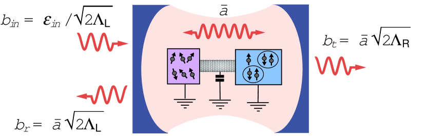
There, corresponds to the contribution of the left(right) port to the cavity linewidth, which implies . From Eq.(35) and Fig.5, the cavity microwave transmission can be expressed as
| (39) |
Hence, in the semiclassical linear limit, the cavity transmission amplitude is set by the charge susceptibility of the nanocircuitCottet:2011 ; Bruhat:2016a ; Viennot:2014a ; Schiro:2014 ; Dmytruk:2015 . A similar result can be obtained for the cavity reflection amplitude. Note that above, is expressed with the usual quantum mechanics convention for the definition of Fourier transforms, i.e. , which is used in this whole review. In order to interpret experiments, one has to take into account that microwave equipment uses the electrical engineering Fourier transform convention, which is complex conjugated to the former, so that is obtained experimentally.
In practice, the experimental signals which are directly measured are the transmission phase shift and amplitude shift defined by
| (40) |
In the limit and , one finds that the cavity signals are directly related to the cavity parameters’ shifts, i.e.
| (41) |
and
| (42) |
so that and correspond to the dispersive and dissipative parts of the signal. Beyond this limit, the experimental data can be understood by combining Eqs.(39) and (40).
Depending on the regime of parameters fulfilled by the nanocircuit, and in particular the order of magnitude of the tunnel rates between the dots and reservoirs, different calculation techniques can be used to calculate . We will discuss several possibilities in the next sections. In this review, we will only consider cases where the summation on indices and in Eq.(36) can be restricted to internal sites of the nanoconductor. This requires that the coupling between the cavity and the nanoconductor sites is much larger than the coupling between the cavity and the reservoirs. This is not a priori obvious since the nanoconductor is much smaller than the reservoirs and thus tends to have a smaller capacitance towards the cavity resonator. However, this feature can be compensated by using for instance ac top gates which reinforce the coupling between the nanoconductor and the cavity. In this limit, corresponds to the charge susceptibility of the nanoconductor at frequency . In the opposite limit where the coupling between the cavity and the source/drain of the nanocircuit is dominant, it has been observed experimentally that the cavity signals essentially show replicas of the conductance signalDelbecq:2011 .
IV Mesoscopic QED experiments in the artificial atom limit
IV.1 Measuring the internal degrees of freedom of a nanocircuit with cavity photons
In this section, we consider a nanocircuit with a very small tunnel coupling to metallic reservoirs. Hence, the nanocircuit behaves as an artificial atom and a direct analogy with Cavity or Circuit QED experiments can be drawn. Assuming that the summation on index in Eq.(30) can be restricted to sites which do not correspond to a reservoir, one gets
| (43) |
Above, is an internal transition frequency of the nanoconductor between states and , is the decoherence rate associated to this transition, and is the average occupation of state . We will see later in a particular example how to derive this expression which is valid for and all transitions frequencies well separated (see section IV.2.2).
We now discuss a measurement of and made with a constant cavity excitation frequency . In the absence of external dc bias voltages, one has necessarily , because the nanocircuit can only damp cavity photons. By combining Eqs.(39), (40) and (43), one can see that the cavity signals are resonant for . In a typical experiment, the transitions frequencies can be tuned with nanocircuit control parameters such as dc gate voltages or the external magnetic field. When these parameters are swept, the cavity signals provide a cut of the nanocircuit excitation spectrum at frequency , as illustrated by Fig.6. For well separated resonances, presents a negative peak at whereas presents a variation with a sign change at (see Fig.6c). Therefore, the excitation spectrum of the nanocircuit is more straightforwardly readable in the signal, in principle.
For quantum information applications, the strong coupling regime between the nanocircuit and the cavity is intensively sought after. This regime corresponds to having one of the nanocircuit transitions such that . We will also assume below that the other nanocircuit transitions do not affect significantly the cavity. For the most simple characterization of the nanocircuit/cavity coupling, the nanocircuit is kept in its ground state (, ). In these conditions, the cavity response is set by the charge susceptibility
| (44) |
with the decoherence rate of the resonant nanocircuit transition, and its coupling to the cavity. In the strong coupling limit, the cavity resonance versus shows two peaks instead of the single peak of the weakly coupled regime, due to the strong hybridization of the cavity states with the nanocircuit states and (see Figure 9d). This regime has already been reached for instance with atomic cavity QEDThompson:1992 ; Brune:1996 , or isolated quantum dots in optical cavitiesReithmaier:2004 ; Yoshie:2004 , or superconducting quantum bits coupled to microwave cavitiesWallraff:2004 . It has also also been reached more recently in Mesoscopic QED, as will be discussed in section 4.2.3
It is useful to define figures of merit to characterize the strength of a light/matter resonance. We first define the cooperativity
| (45) |
From Eq.(39), in the resonant regime , this figure of merit indicates whether the cavity dissipation is dominated by the intrinsic cavity damping () or by the nanocircuit dissipation (). The cooperativity can also be used to express the lasing threshold to obtain a lasing effect with a single qubit in a cavity, in a situation where and the qubit dephasing is much stronger than the qubit relaxation ( so that ) (see for instance Refs.Andre:2006 ; Andre:2010 ).
In the devices considered in the present review, is always fulfilled due to the high quality of the resonators used. In this context, the ratiodefC
| (46) |
is also instructive. For a resonant cavity/nanocircuit transition () and in the limit of a negligible bare cavity linewidth, two resonance peaks are visible in the cavity response as soon as . Below, we discuss various circuit geometries where the transition corresponds to charge, spin or electron/hole degrees of freedom. The values of and obtained for in these different cases are presented in Table 1.
IV.2 Charge double quantum dots with normal metal contacts
IV.2.1 Hamiltonian of the device
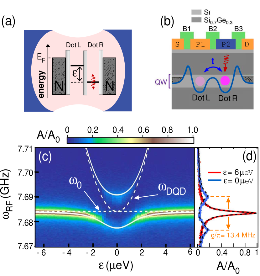
The case of a double quantum dot embedded in a microwave cavity has received a lot of experimental attention Frey:2011 ; Frey:2012a ; Petersson:2012 ; Schroer:2012 ; Frey:2012b ; Toida:2012 ; Toida1:2013 ; Basset:2013 ; Delbecq:2013 ; Zhang:2014 ; Viennot:2014a ; Basset:2014 ; Wang:2016 ; Schroer:2012 ; Deng:2015 .. The intrinsic level separation between the orbitals of one dot (see Eq.(1)) is usually very large in comparison with the other energy scales of the device. Therefore, it is sufficient to consider a single orbital with energy in dot . These two orbitals are coupled with a hopping constant . In practice, each dot is also contacted to a normal metal reservoir, which enables one to control and measure the double dot charge. One can use the energy diagram of Fig.7, where the Fermi levels in the reservoirs are filled up to the Fermi energy and the orbital levels of the two dots have an energy separation . This last parameter can be controlled with the gate voltages and shown in Fig.8.
It is possible to tune and such that there is a single electron in the double dot due to Coulomb blockade. In the spin-degenerate case, the spin degree of freedom can be disregarded to describe this situation since the two spin species play the same role and are not present simultaneously in the double dot. Therefore, the only internal degree of freedom relevant to describe the internal dynamics of the double dot in this limit is the left/right charge degree of freedom. In this framework, the double dot Hamiltonian writes
| (47) |
where forbids the double occupation of the double dot. Using the basis of bonding and antibonding states of the double dot, one gets
| (48) |
with the double dot transition frequency. Above, we have used the creation operators
| (49) |
and
| (50) |
for bonding and antibonding states in the dot, and the parameter .
In most experiments designed so far, the samples have been designed with an asymmetric coupling of the two dots to the cavity, in order to modulate the parameter with the cavity electric field (see for instance Figure 8a).
In this case, following section III.1.6, the interaction term between the double dot and the cavity can be expressed as
| (51) |
with . Using a rotating wave approximation, this term can be expressed as
| (52) |
with
| (53) |
This coefficient depends on the differential coupling because the coupling to the cavity occurs through the modulation of the dot orbital detuning .
As we have seen in the previous section, in order to obtain the strong coupling regime, one needs to have a small enough . The coherence of a charge double dot is mainly limited by charge noise due to charge fluctuators which move in the vicinity of the double dot. This induces fluctuations of the parameters which are electrically controlled, i.e. in the present case. This effect should be minimal at the charge noise sweet spot where , similar to what has been done for early days charge superconducting quantum bits which are also affected by this problemCottet: 2002 . Hence, it would be interesting to perform a systematic study of the figures of merit of the cavity/double dot resonance when the double dot parameters, and in particular , are varied.
In principle, the coupling of a double-dot dot to a microwave cavity can be mediated by other variables than , depending on the sample design. The first manipulations of the quantum state of a double dot were performed by modulating the parameter with a strong classical driveHayashi:2003 . Recently, similar experiments were performed by modulating the interdot tunnel parameter Bertrand:2015 ; Reed:2016 ; Martins:2016 , along the theory proposal of Ref.Loss:1998 . One could push further this idea by building ac gates connecting the double dot barrier to the cavity central conductor, in order to modulate the interdot tunnel parameter with the cavity electric field. In principle, this could enable one to obtain double dots with a better coherence, since the electric (and charge noise) control of the variable can be shunted, in this case. In section IV.4, we will discuss an alternative strategy to control electrically which consists in using a superconducting contact.
IV.2.2 Master equation description
This section shows how to calculate the cavity charge susceptibility of the double dot when a microwave cavity is coupled to a single transition which corresponds to the left/right charge degree of freedom of a double quantum dot. The dynamics of this mesoscopic QED device can be described by using a master equation approach (or Lindbladt formalism) already widely used for Cavity or Circuit QEDCohen-Tannoudji:book1 . From Eqs. (28), (47) and (52), one gets
| (54) |
| (55) |
with the total decoherence rate of the double dot transition, which includes relaxation and dephasing effects. Importantly, the above equations are valid for . In the semiclassical limit with , one can use Eq.(32) and the resonant expression
| (56) |
Hence, Eqs. (54) and (55) give
| (57) |
with and the average occupation numbers of the bonding and antibonding states. A comparison with Eq.(35) gives
| (58) |
The above equation corresponds to a well known result in the dispersive regime where can be disregarded (see for instance Ref.Blais:2004 ). In this limit, depending on whether the nanocircuit is in the state or , the cavity shows a frequency pull . This can be used to read out the state of the nanocircuit in a nondestructive way, since in this limit, accounts for second order processes which do not change the state of the nanocircuit. This method is widely used to read out the state of superconducting quantum bitsWallraff:2004 . In section IV.2, we consider double dots with no voltage bias, and we also assume that the dot levels are not resonant with the normal metal reservoirs, so that the electron which is trapped in the double dot cannot escape. We also assume that the power of the microwave tone applied to the cavity is too low to excite the transition between the bonding and antibonding states. In this case, at equilibrium, one has and , which leads to Eq.(44).
IV.2.3 Experimental results
Weak coupling limit
The resonance between a closed charge double-dot and a microwave cavity in the linear coupling regime has been measured by many groups, with different types of nanoconductors and grounded normal metal reservoirs. In all these experiments, the differential coupling between the double dot and the cavity is reinforced thanks to a local ac gate connected only to one dot. First experiments have revealed a very weak light matter coupling, i.e. (see Table 1 for various examples). Figure 8 shows an example of experimental data obtained with a double dot made in a carbon nanotubeViennot:2014a , with an average photon number in the cavity . If , one has for any value of so that the double dot and cavity are always off resonant and the signals and show broad responses centered on (not shown). For , two resonances between the cavity and the double dot are expected when varies, for (see Fig.8b). As expected from Eq.(58), shows two sign changes along the axis, corresponding to these two resonances (Fig.8c), whereas keeps a constant negative sign and shows two simple resonances (Fig.8d). From the cavity signals of Fig.8, one can determine and at . With , this gives and . Therefore, the strong coupling regime is far from being reached in this experiment.
In spite of a weak electron-photon coupling, it is possible to obtain interesting photon emission effects by applying a strong microwave drive to a double dot. This was shown recently with an InAs double dot. The same electron trapped in the double dot is repeatedly driven to the excited state by a microwave excitation with a strong amplitude which is off resonant with the cavity and applied directly on the double dot gates. This generates a double dot population inversion. which leads to cavity photon emission or absorption, with a rate which depends on the double dot and cavity dynamics but also on the dissipation caused by phonons in the InAs nanowireStehlik:2016 .
Strong coupling limit
Very recently, the strong coupling regime was reached simultaneously in three experiments based on different types of charge double quantum dotsMi:2017 ; bruhat:2017 ; Stockklauser:2017 . In this regime, for a low number of photons , the cavity transmission (or reflection) amplitude versus the frequency excitation shows a double peak, due to the strong hybridization between the cavity and the L/R charge degree of freedom of the double dot (see Fig.9d). To reach this regime, the differential light-matter coupling must be sufficiently large in comparison with the decoherence rate of the L/R degree of freedom, which is typically dominated by dephasing due to charge noise. In this case, the dephasing rate of the charge double dot takes the formViennot:2015
| (59) |
where is the local charging energy of one dot (we disregard the mutual charging energy between the dots). Above, is the dimensionless prefactor in the noise spectrum which adds up to the reduced gate charge with the capacitance between dot and its gate voltage source with voltage . From Eqs. (46), (53) and (59), in order to have , three different technical strategies are possible: either use a nanoconductor technology with an intrinsically lower charge noise (i.e. decrease ), or use a double dot with. larger capacitances (i.e decrease ) in order to shunt the effect of charge noisebruhat:2017 , or change the cavity technology in order to increase the cavity electric field and thus the factorStockklauser:2017 . These three strategies have already been implemented experimentally, as discussed in the paragraphs below. In all cases, using a device with should be advantageous, so that is only a second order effect in when the device is tuned at the anticrossing between the cavity and the double dot (one has and thus )
In Ref Mi:2017 , a double quantum dot in an undoped Si/SiGe heterostructure was used (see Fig.9b). When the double dot is far off resonant with the cavity, a single resonance is visible along the axis, which corresponds to the bare cavity resonance (see blue line in Fig.9c). When is used, and when the double dot is tuned near its sweet spot (), the vacuum Rabi splitting is observed, i.e. a double cavity resonance is visible along the axis (see red line in Fig.9c). In this device, the charge-photon coupling is comparable to what has been obtained with other charge double dots (see Table 1). The microwave cavity is also similar to the ones used in previous experiments, with . The vacuum Rabi splitting is achieved thanks to an unusually small decoherence rate of the left/right charge degree of freedom in the double dot. This gives light-matter coupling ratios and . In the Si/SiGe two-dimensional structure used for this experiment, the dot charging energies are typically of the order of Mi:2016 . In comparison, the GaAs/AlGaAs structure of Ref.Stockklauser:2015 has smaller charging energies , but it is far from the strong coupling regime. This suggests that the low value in Ref.Mi:2017 might be due to a much lower intrinsic charge noise in Si/SiGe devices. In agreement with this, in GaAs/AlGaAs devices, one of the smallest reported value of charge noise is Petersson:2010b is , whereas the values have been reportedFreeman:2016 for doped Si/SiGe heterostructures. Undoped Si/SiGe heterostructures might have an even lower charge noiseObata:2014 . The value of charge noise in Si/SiGe deserves a thorough investigation in order to confirm this picture.
Ref.Stockklauser:2017 has used a GaAs/AlGaAs heterostructure similar to in Ref.Stockklauser:2015 . However, the coplanar waveguide architecture has been modified by replacing the central resonator of the cavity by an array of 32 SQUIDs (Superconducting QUantum Interference Devices). This increases by a factor the couplings . One has , and which gives and . These figures of merit are very close to those of Ref.Mi:2017 . However, they have not been obtained at the double dot sweet spot since was used. This could suggest that the above figure of merits are not the optimal ones for this setup. Interestingly, with the SQUID array architecture, the cavity frequency can be tuned by using an external magnetic field. However, the cavity decoherence rate is stronger with this architecture ().
Alternatively, Ref.bruhat:2017 has reached the strong coupling regime to the left/right charge degree of freedom of a double dot by using a device with small charging energies. However, the double dot has a fundamentally different architecture in this experiment, since it comprises a superconducting contact, and since the coupling to the cavity photons seems to occur through the variable instead of . Therefore, we will discuss this experiment in section IV.5.
IV.3 Mesoscopic QED with spins in quantum dot circuits
IV.3.1 Spin-photon coupling due to spin-orbit coupling
The electronic spin degree of freedom draws a lot of interest in nanoconductors because it could be a good means to encode quantum information. Indeed, spins are expected to have a long coherence time in nanoconductors because they are more weakly coupled to their environment than charges. The counterpart of this immunity is that the natural magnetic coupling between a spin and a standard coplanar microwave cavity is only a few Hz, which is not sufficient for manipulation and readout operations. It is possible to circumvent this difficulty by using a large number of spins, as demonstrated recently with several types of crystals coupled to coplanar microwave cavitiesSchuster:2010 ; Kubo:2010 ; Zhu:2011 . However, in this case, the anharmonicity which is inherent to a two level system is lost so that the spin ensemble can only be used as a quantum memory. To remain at the single spin level, it has been suggested to include in the microwave cavity a nanometric constriction to concentrate the cavity field, which would yield kHz Tosi:2014 ; Haikka:2017 . Alternatively, various theory Refs. have suggested to use a weak hybridization between the spin and charge degrees of freedom of a quantum dot circuitTrif:2008 ; Hu:2012 ; Kloeffel:2013 ; Beaudoin:2016 ; Cottet:2010 , provided by a real or artificial spin-orbit coupling. To understand this effect, let us assume that the state of the dot circuit can be decomposed on a basis of pure spin eigenstates states and with an orbital index. In the presence of a spin-orbit coupling term the Hamiltonian of the dot circuit will write:
| (60) | ||||
Above, is the orbital energy of state , is the external Zeeman field applied to the circuit, and corresponds to the matrix elements of the spin-orbit interaction on the basis of states . The photonic pseudo potential is spin-conserving, so that the light-matter interaction given by Eq.(20) is
| (61) |
Hence, at first order in spin-orbit coupling, the eigenstates
| (62) |
of are coupled to the cavity with the matrix element
| (63) | |||
One can imagine to build a qubit by using two states and which can be considered as quasi-spin states if the spin-charge hybridization is small. Due to this hybridization, this qubit will be sensitive to charge noise. Therefore one has to choose a design which establishes a good compromise between having a small enough decoherence and a high enough light-matter-coupling.
In principle, from Eq.(63), a single quantum dot with a natural Rashba or Dresselhaus spin-orbit coupling could already offer a spin-photon interaction. Indeed, the spin of a quantum dot was manipulated by using a large ac drive applied directly on the dot gate and coupled to the spin through the spin-orbit couplingNowack:2007 ; Liu:2014 . One can imagine to replace the direct ac drive by the cavity field. Then, the indices , in the above equations can correspond to the natural subbands in the dot spectrum. However, for most quantum dots, the spin-orbit interaction is too weak to enable the strong coupling regime with a single quantum dot circuit. For instance, for GaAs quantum dots, it has been shown theoretically that the effect of spin-orbit coupling is limited by the small spatial extension of the quantum dotKhaetskii :2000 ; Khaetskii :2001 ; Erlingsson:2002 . As we will see in section IV.3.3, an alternative approach is to engineer extrinsically an artificial spin-orbit coupling by using a quantum dot circuit with ferromagnetic contacts, which induce local effective Zeeman fields such as those of Eq.(2). Then, it is not necessary to invoke the existence of several levels in each dot. For instance, in the case of a double quantum dot, the indices , can be restricted to a pair of bonding and antibonding states, formed by the coherent coupling of left and right orbitals of the double dot. In principle, this should enable one to tune the value of the spin-orbit interaction, thanks to the electric control of the orbital energy detuning . Another interesting possibility could be to use designs which exploit stray fields from micromagnetsTokura :2006 ; Takeda:2016 .
IV.3.2 Charge readout of spin-blockaded states in a double dot
As shown in section IV.2, internal tunnel hopping of charges inside a double quantum dot modifies the cavity signals. This property can be used to detect with a dc current measurement the spin state of a pair of electrons trapped in a double quantum dot, thanks to a spin-rectification effect induced by Pauli spin blockade, which has been widely studied through current measurements Ono: 2002 . This effect was recently exploited in a Mesoscopic QED device, based on a singlet-triplet qubit in an InAs double quantum dot, with one electron in each dotPetersson:2012 . The readout of this qubit requires to discriminate the two states and . When the orbital detuning between the left and right dot is modulated by the cavity electric field, transitions to the state are possible only if the double dot initially occupies the state , due to the spin-conserving character of interdot tunneling. This leads to . In contrast, if the double dot is in the state , one has due to the Pauli exclusion principle. Therefore, the spin state of the double dot can be detected through the cavity signals. It is nevertheless important to point out that a direct spin-photon coupling was not implemented in the experiment of Ref.Petersson:2012 . The state of the double dot was manipulated by applying a strong microwave drive directly to the dots gates, to rotate the spins thanks to spin-orbit coupling. The cavity was used only to perform the charge readout of the spin qubit. To date, no experiment could detect a spin-cavity coupling caused by intrinsic spin-orbit coupling in a nanocircuit.
IV.3.3 Spin-photon coupling in a double quantum dot with non-collinear ferromagnetic contacts
It was recently suggested that the coupling of Eq.(63) could be realized by using a double quantum dot with two ferromagnetic contacts magnetized in non-collinear directionsCottet:2010 , represented in Fig.10a. These contacts cause a spin-mixing of the double dot eigenstates, which can be viewed as an artificial spin-orbit coupling. This effect occurs due to intradot effective Zeeman fields similar to those of Eq.(2). By tuning the orbital detuning , one can in principle control the degree of delocalization of the electron between the two dots, in order to tune the magnitude of the artificial spin-orbit interaction.
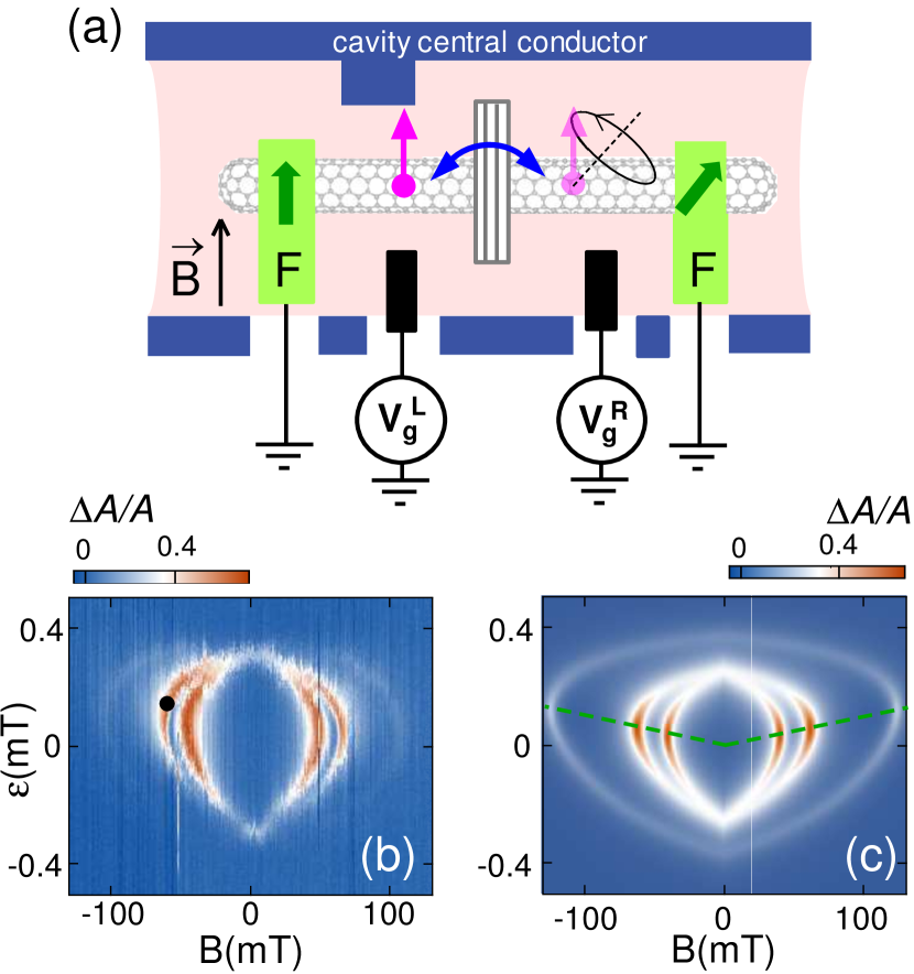
A first version of this device has been realized recently, by using a double quantum dot made in a single wall carbon nanotube on top of which two ferromagnetic PdNi contacts are evaporatedViennot:2015 . When the microwave transmission amplitude of the cavity is measured versus and the external magnetic field applied to the double dot, three resonant lines appear (see Fig.10b). Various features suggest that the spin degree of freedom is an important ingredient in this pattern. First, the resonances split and strongly move with the external magnetic field , with a maximum of contrast/coherence for a finite value of . Second, the black point of Fig.10b corresponds to a coupling and a double dot decoherence rate . This last number is about 200 smaller than the charge decoherence rate determined for a similar carbon nanotube device (see section IV.2.3). One has which means that this device is almost in the strong coupling regime.
To understand better the contribution of the spin degree of freedom to the cavity signals, one can use Eq.(43) which is a generalization of Eq.(58), valid if the different transition frequencies of the nanocircuit are well separated. To calculate and the couplings , one has to use a double dot Hamiltonian which takes into account the existence of the left/right and spin degree of freedoms of the double dot, but also the K/K’ local orbital degree in each dot (or valley degree of freedom), which is due to the fact that electrons can rotate clockwise or anticlockwise around the carbon nanotube. The linewidth of the resonances can be modeled by taking into account the effect or charge noise. This gives Fig.10c, which reproduces well the behavior of Fig.10b. The two strongest resonances mainly correspond to spin transitions with a conserved K/K’ index. These two resonances are slightly split due to a small lifting of the K/K’ degeneracy. The third weaker resonance mainly corresponds to a transition where both the spin and the K/K’ index are reversed. In Fig.10c, this transition is less visible than the two others because the K/K’ degree of freedom is only weakly coupled to cavity photons, probably due to weak microscopic disorder in the carbon nanotube structure. However, this resonance is very interesting in the light of recent works which investigate the coupling between the valley degree of freedom of a silicon dot and a microwave cavity Burkard:2016 ; Mi:2017b .
Remarkably, the coherence (or, visually, the contrast) of the three transitions is maximum along the green dashed line in Fig.10c. This is because the derivative of the transition frequencies with respect to vanishes along this line, which is a charge noise sweet line. This behavior also occurs in the data, which confirms that charge noise is an important source of decoherence in this device. It may be possible to enhance these performances by reducing the spin-charge hybridization to decrease decoherence due to charge noise. It is expected that will decrease more quickly than with , so that the strong coupling regime is accessible with this geometry, in principleCottet:2010 .
IV.3.4 Spin-photon coupling in multiple particle devices with collinear fields
Various theory Refs. have suggested to couple electrically the spin degree of freedom to the cavity electric field by using two or three electron states in a quantum dot circuit. For that purpose, one can use a multi-quantum dot circuit with proper spin-symmetry breaking ingredients, in order to transduce the charge-photon into a spin-photon coupling. For instance, in a double dot with a finite interdot hopping, the transition between the singlet and triplet spin states and is coupled to cavity photons due to the presence of a Zeeman field with constant direction but a different amplitude in the two dotsPeiQing:2012b ; Pei-Qing:2016 ; Burkard:2006 ; Wang:2015 ; Han:2016 . This field can correspond to an Overhauser field due to nuclear spins in a two-dimensional electron gas, or to stray fields from a ferromagnet. In the case of a triple quantum dot, it is possible to use three electron states from the subspace, with the total spin of the dots, to define the resonant exchange qubitRuss:2015 ; Srinivasa:2016 ; Russ:2016 . In this case, the spin-photon coupling can be obtained with a homogeneous Zeeman field if the spatial symmetry of the triple dot is adequately broken. Note that the above setups do not involve any real or effective spin-orbit interaction. On the contrary, they consider devices where the individual spin of electrons would be conserved in the single electron regime. At present, the multiparticle spin-photon coupling of Refs.PeiQing:2012b ; Pei-Qing:2016 ; Burkard:2006 ; Wang:2015 ; Han:2016 ; Russ:2015 ; Srinivasa:2016 ; Russ:2016 is awaiting an experimental realization.
IV.4 Probing Andreev states with cavity photons
When superconducting elements are included in a nanocircuit, the electron and hole excitations become coupled by Andreev reflections, so that Andreev bound states appear inside the nanoconductors (see Fig.2c). This superconducting proximity effect raises a strong attention presently because it is at the heart of phenomena such as Majorana bound states in hybrid structures or Cooper pair splitting. Furthermore, Andreev bound states can appear on interfaces such as an atomic contact, for which the charge orbital confinement is not a relevant concept. One could hope that such states are weakly sensitive to charge noise and could be a good support of quantum information. It is therefore very interesting to investigate the properties of this degree of freedom with a microwave cavity, as suggested by Ref.Skoldberg:2008 . In the presence of superconductivity, the Hamiltonian of the hybrid nanocircuit can be written as
| (64) |
with and a Bogoliubov-De Gennes excitation creation operator which is a superposition of and operators. Hence, the interaction term with the cavity takes the general formCottet:2015
| (65) |
In the absence of magnetic coupling between the device and the cavity, the elements and can be expressed as matrix elements induced by the cavity photonic pseudopotential between the wavefunctions associated to and (see Ref.Cottet:2015 for details). At zero temperature (), Eq.(65) givesDartiailh:2016
| (66) |
Importantly, due to the Pauli exclusion principle, one has since a term in cannot occur in . Hence, from Eq.(66), does not involve transitions between electron and holes states associated to conjugated operators and Dartiailh:2016 ; Vayrynen . This selection rule can be extended to a finite temperature () or a level broadening smaller than the inter-level separationDartiailh:2016 . Nevertheless, having a nanocircuit response at is possible provided there exists a state degeneracy in the nanocircuit so that a coefficient comes into playSkoldberg:2008 , as observed in spin-degenerate superconducting atomic contactsJanvier:2015 . In this experiment, an atomic contact between two superconductors was coupled to a microwave resonator through a superconducting loop. A light matter coupling and a decoherence rate were estimated inside a spin-degenerate Andreev doublet, which corresponds to and . These good performances are probably related to a smaller sensitivity of atomic point contacts to charge noise.
Interestingly, devices have been built, where a microwave cavity is coupled to a superconducting circuit which includes a Josephson junction made out of a semiconducting nanowire quantum dotLarsen:2015 ; Lange:2015 . The superconducting current in the Josephson junction is mediated by Andreev bound states inside the quantum dot. Since the spectrum of Andreev states is tunable with the dc gate of the dot, the critical current of the Josephson junction is electrically controllable. This can represent a technical advantage in comparison with usual magnetically tunable Josephson junctions made out of a SQUID. The nanowire junction is used to form the ”Gatemon” superconducting quantum bit which involves a coupling between a microwave cavity and the superconducting phase difference between two metallic islandsLarsen:2015 ; Lange:2015 . This variable is a macroscopic collective degree of freedom of the superconducting circuit. Therefore, these devices belong more to the family of Circuit QED devices than to the family of Mesoscopic QED devices. This is why we will not discuss them further in this review.
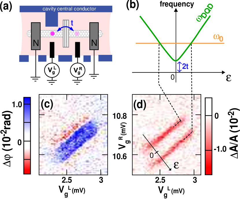
IV.5 Double quantum dot with a central superconducting contact
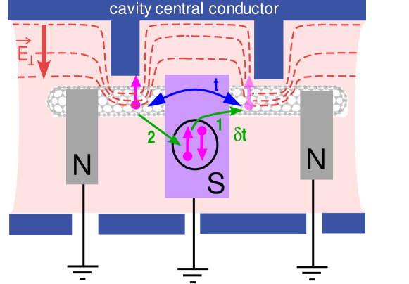
Recently, the coupling scheme between a double quantum dot and a cavity was drastically modified by placing a superconducting contact between the two quantum dots instead of an insulating barrier, and two identical ac top gates on the two quantum dotsbruhat:2017 (see Figure 11), instead of coupling asymmetrically the two dots to the cavity as done usually (see Fig.1). In the symmetric coupling case of Fig. 11, the differential coupling between the two dots and the cavity is expected to be small. However, anticrossings were observed in the cavity response for a low number of photons in the cavity. These anticrossings can be switched on/off with the double dot gate voltages, and they vanish when the photon number is large so that the double dot transitions are saturated. This suggests that the cavity anticrossings are due to a strong coupling between the cavity and the double dot. A fitting of these anticrossings yields a coupling and a decoherence rate which corresponds to and .
| Geometry | double dot material |
|
cavity design | Refs. | Fig. |
|
|
|
|||||||||||
| N/dot/dot/N | graphene | charge | Al stripe | Deng:2015 ; NoteDeng | |||||||||||||||
| N/dot/dot/N | InAs nanowire | charge | Nb stripe | Liu:2014 ; NoteLiu | |||||||||||||||
| N/dot/dot/N | carbon nanotube | charge | Al stripe | Viennot:2014a | 8 | ||||||||||||||
| F/dot/dot/F | carbon nanotube | quasi-spin | Nb stripe | Viennot:2015 | 10 | ||||||||||||||
| N/dot/S/dot/N | carbon nanotube | charge | Nb stripe | bruhat:2017 | 11 | ||||||||||||||
| N/dot/dot/N | GaAs/AlGaAs 2DEG | charge | Al stripe | Stockklauser:2015 | 17 | ||||||||||||||
| N/dot/dot/N | GaAs/AlGaAs 2DEG | charge | Al SQUID array | Stockklauser:2017 | |||||||||||||||
| N/dot/dot/N | Si/SiGe 2DEG | charge | Nb stripe | Mi:2017 ; NoteMi | |||||||||||||||
| S/atom/S | Al atomic contact | Andreev state | Nb stripe | Janvier:2015 | 9 |
This result may seem surprising since a standard coupling to the left/right charge degree of freedom through the variable is unlikely for a small . However, two ingredients can help to understand the behavior of the setup. First, due to the superconducting gap, direct dissipative tunneling between the dot and the superconductors is forbidden, but second order tunnel processes from one dot to the other are allowed. This gives a renormalization of the tunnel coupling between the two dots which depends on the average orbital energy . This last parameter is well coupled to cavity photons even when . A coupling between the left/right degree of freedom of the double dot and the cavity photons can thus be restored. Second, there is a large capacitance between the dots and the ac top gates, so that the dot charging energies are decreased by a factor (determined from conductance measurements) in comparison with the experiment of Fig.8. This strongly reduces the sensitivity of the device to charge noise. This strategy is reminiscent from the strategy developed for the Transmon superconducting quantum bit. In this device, a very large charging energy is used to flatten the dispersion of the energy bands with gate voltages and reduce the sensitivity to charge noiseKoch:2007 .
IV.6 Comparison between the different systems and conclusion
Table I presents a comparison of the performances of the different Mesoscopic devices used to far to implement artificial atoms in a cavity. Impressive progresses are already visible since the publication of the first experiments in Refs.Delbecq:2011 ; Frey:2011 . To summarize, charge and spin states in a double quantum dot, and Andreev bound states in atomic contacts have been strongly coupled to cavity photons. First experimental results are also available regarding the local orbital degree of freedom in a quantum dot, for Si/SiGe heterostructuresMi:2017b , and carbon nanotube devicesViennot:2015 . Other configurations have been proposed theoretically which lack experimental realization, at present. For instance, it has been suggested to use multiparticle spin states in devices with no spin-orbit couplingPeiQing:2012b ; Pei-Qing:2016 ; Burkard:2006 ; Wang:2015 ; Han:2016 ; Russ:2015 ; Srinivasa:2016 ; Russ:2016 . It could also be interesting to use Shiba states which are Andreev states in the presence of a magnetic impurity or strong Coulomb interaction in a quantum dotChirla:2016 . Interestingly, several theoretical works have proposed manipulation protocols which circumvent at least partially the imperfections of Mesoscopic QED devices, and in particular a limited coherenceWang:2015 ; Beaudoin:2016 ; Schuetz:2016 .
V Mesoscopic QED experiments beyond the artificial atom limit
In the previous sections, we have shown that cavity photons are a powerful probe for the internal dynamics of a nanoconductor. The present section will show that a microwave cavity is also a very interesting tool to study the dynamics of tunneling between a nanoconductor and a metallic reservoir. The interplay between electron tunneling to reservoirs and the light matter coupling leads to a very rich phenomenology Xu:2013a ; Schiro:2014 ; Hartle:2015 ; Wong:2016 ; Cirio:2016 ; Dmytruk:2016 ; Agarwalla:2016 ; Kumar:2016 whose experimental investigation with microwave cavities has recently started.
V.1 Keldysh expression of the charge susceptibility of a nanocircuit
In section IV, the nanocircuit charge susceptibility which sets the cavity signals in the linear semiclassical limit, was evaluated without taking into account explicitly tunnel processes towards the fermionic reservoirs of the nanocircuit. Hence, it is useful to introduce a more general calculation method for . For simplicity, we will assume that the coupling of the cavity to the fermionic reservoirs of the nanocircuit is negligible. In case of a quantum dot circuit, the cavity electric field simply modulates the potential of some quantum dots with a coupling constant , like in Eqs.(28) and (30). Alternatively, in case of a one-dimensional conductor, a coarse grain description into sites with an index can be usedDartiailh:2016 . Then, in the semiclassical limit, the cavity signals (37) and (38) are set by the nanocircuit charge susceptibility , defined by Eqs. (34) and (36). Disregarding Coulomb interactions in the dots/sites, this quantity can be expressed by using the Keldysh formalism as
| (67) |
with
| (68) |
Above, and are the retarded and advanced Greens’ functions of the dots or nanocircuit internal sites. These Green’s functions have a matrix structure with elements with
| (69) |
Above, , are quasiparticle creation and annihilation operators inside a site of the nanoconductor and denotes an average calculated with the light-nanocircuit interaction turned off. The matrix is a diagonal matrix which corresponds to in the orbital block . The derivation of Eq.(67) is given in appendix VII. The matrix structure of takes into account the sites and spin degrees of freedom of electrons and also the electron/hole degree of freedom if the nanocircuit includes superconducting elements (a few examples of will be presented in the next sections). The self energy has a matrix structure similar to , and it involves Fermi occupation factors of the fermionic reservoirs. The tunnel rates to the reservoirs affect the values of both and , as we will see in various examples in the next sections. One advantage of the Keldysh approach is that it is very general. It can be used to describe the presence of many different types of reservoirs, such as normal metals, superconductors or ferromagnets, with possibly finite bias voltages leading to non-equilibrium transport effects. It also takes into account properly internal hopping between neighboring dots or sites, which leads to the internal transitions discussed in section IV. For instance, Appendix B shows how to recover an expression of the charge susceptibility of a closed non-interacting double quantum dot similar to Eq.(58), by using Eq. (67). Other examples of use of Eq.(67) are given in sections V.2, V.3 and V.5.3.
V.2 Effective admittance of a single quantum dot with normal metal contacts
The simplest possible example of open quantum dot circuit which can be coupled to a microwave cavity is a single level quantum dot with a normal metal reservoir. This situation has been studied experimentally with carbon-nanotube quantum dotsDelbecq:2011 ; Bruhat:2016a . It is possible to control electrically the energy detuning between the dot level and the Fermi energy of the reservoir (see Fig. 13a). The signals and were measured as a function of for several dot levels with a different tunnel rate between the dot and the normal metal reservoir (see Figure 13, bottom panels, which represents the opposites of and ). For , the signal is very small while is always negative with a minimum at (see Fig.13A). For , seems globally larger but negative in any case, whereas changes sign and becomes positive around (see Fig.13C).
To understand this behavior, one can model the device with Hamiltonian (28) with
| (70) |
and
| (71) |
Above, is the tunnel hopping parameter between the dot and the reservoir, and the coupling of the dot level to cavity photons. The spin index is . The tunnel rate between the dot and the reservoir can be expressed as .
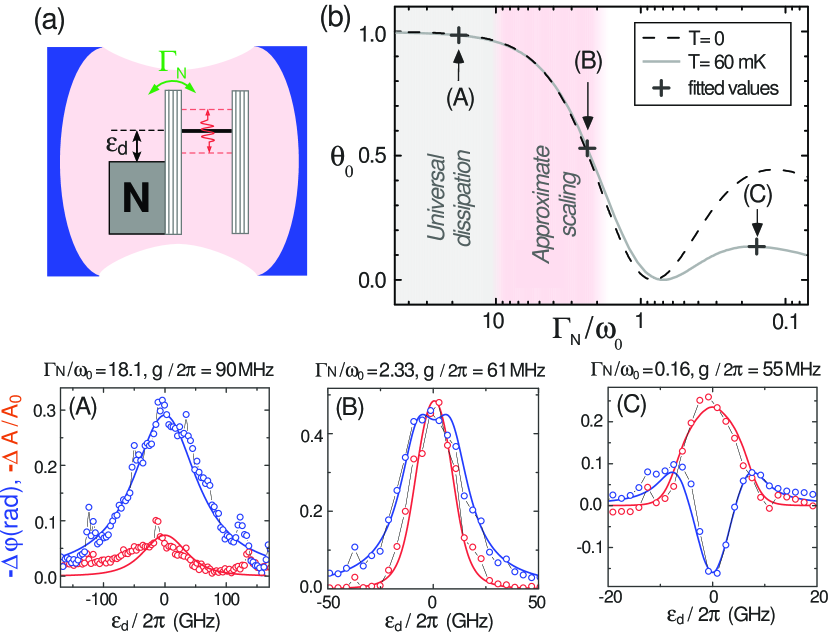
One can use the non-interacting Keldysh formalism of section V.1 to calculate the charge susceptibility which corresponds to Eqs.(70) and (71). Here, we define
| (72) |
Equation (70) then gives
| (73) |
and
| (74) |
with and the identity matrix in spin space. In this diagonal case, it is possible to reduce the number of Green’s function in expression (67) by using the identity
| (75) |
This leads to the result
| (76) |
with
| (77) |
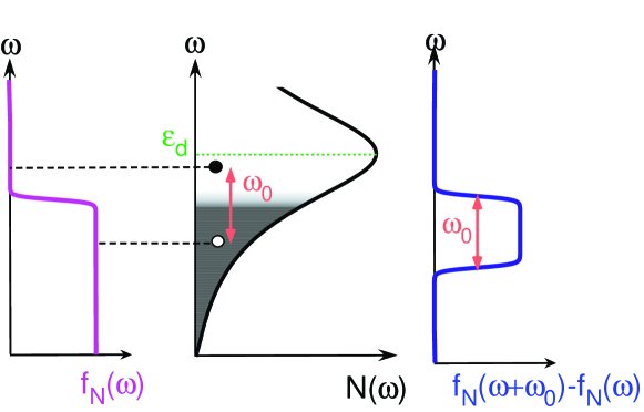
Since the current through the tunnel junction corresponds to the time derivative of the charge on the dot, naturally corresponds to the admittance of the dot. Interestingly, the interpretation of the expression (77) is straightforward: is due to the creation of electron hole pairs at energies and respectively, in the density of states (DOS) of the dot broadened by . This creation is possible if the state at frequency has a low occupation probability whereas the other state at has a high occupation probability. This is taken into account by the difference of fermi factors in Eq.(77) (see Fig.14).
Using Eq.(76), it is possible to reproduce quantitatively, the data of Fig.13A, B, and C. In particular, the sign change in when decreases can be reproduced. Physically, for large tunnel rates , the dot is able to absorb or emit electrons very quickly in response to the modulation of its potential by the cavity field. The dot thus behaves as an effective capacitor. Considering the cavity as a (L,C) resonator in parallel with this effective capacitor, this gives . This behavior can be reproduced with a simple quasi-static model. In the semiclassical and resonant limit with , one has , with is the average equilibrium value of for , because the dot charge has the time to reach its equilibrium value at each time. Therefore, one has
| (78) |
Hence, from Eqs. (37) and (38), one gets a cavity frequency shift which is minimum for , in full agreement with Fig. 13A. In contrast, for small tunnel rates , there is a lagging effect in the charge current because the charge of the dot cannot follow instantaneously the level oscillation caused by the cavity field. Hence, the dot has an inductive behavior which naturally leads to (see 13C). Note that this capacitive to inductive cross-over has also been observed in Ref.Frey:2012a .
The dissipative part of the cavity response in Fig.13 might seem less interesting since it displays no sign change. However, many theoretical studies on the charge relaxation resistance in single quantum dots reveal a surprising universal charge relaxation resistance. This effect was first predicted by Markus Büttiker two decades agoButtiker:1993 ; Pretre:1996 for a non-interacting quantum dot tunnel contacted to a normal metal reservoir and capacitively coupled to an ac voltage source with frequency . In this case, for low frequencies , the quantum dot circuit is expected to behave like a circuit with a constant resistance , independently of the circuit parameters. One can recover this result from Eq.(77). More precisely, in the limit , one finds that can be written in the form which corresponds to the expansion of the admittance of a circuit at low frequency withButtiker:1993 ; Pretre:1996
| (79) |
independently of the circuit parameters and . From Eqs. (37) and (38) and (76), for the device of Fig.13a, the universality of the charge relaxation resistance is equivalent to having a ratio
| (80) |
equal to for any value of Remarkably, this implies that the variations of and with should be similar since and should not depend on .
The value was experimentally confirmed for a two dimensional electron gas structure subject to a high magnetic field measured without a cavity, through a direct ac conductance measurementGabelli . In this case, a similar phenomenology is expected, with divided by a factor 2 and multiplied by a factor due to the lifting of the spin degeneracy. However, the independence of from could not be checked in this experiment. The data of Figs 13 are consistent with this behavior since they can be fitted by the Eqs.(39), (67) and (73)-(77) (see full lines), which give Eq.(79) in the limit . Figure 13b shows the values of calculated from this theory at for the three resonances of the bottom panels. This shows that a broad range of frequency regimes could be addressed with this sample. The universality of is expected in the gray area of Fig.13b where . In the pink area of Fig.13b, one expects . The absolute value of could not be measured in Ref.Bruhat:2016a , but it was found that, in the pink area, the curves and versus show similar variations (see Ref.Bruhat:2016a for details). The scaling of the and curves in the gray area could not be studied accurately due to experimental noise. A further investigation of this regime would be very interesting.
Surprisingly, the data of Fig.13 could be interpreted with a non-interacting theory, although Coulomb blockade was visible in finite bias voltage measurements (not shown). Hence, it would be interesting to understand to which extent the universality of the charge relaxation resistance is robust to interactionsNigg:2006 ; Mora:2010 ; Hamamoto:2010 ; Filippone:2011 ; Alomar:2016 . There is not yet a full consensus on this question and the answer could depend on the regime of parameter considered. Mesoscopic QED experiments provide a new tool to study this question.
V.3 Photon emission by a superconductor/quantum dot interface
So far, we have discussed configurations in which the nanocircuit embedded in the microwave cavity is not voltage biased. However, the combination of the light-matter interaction and the out-of equilibrium dynamics in a voltage-biased nanocircuit can lead to unique features. This is well illustrated by the case of a superconductor/quantum dot/ normal metal bijunction embedded in a microwave cavity. Fig.15a shows the cavity dissipative signal versus the gate voltage of the dot, which shifts the energy level , and versus the finite bias voltage applied to the normal metal contact. An area with appears (see blue area in Fig.15a). This suggests that the bijunction emits photons for some regimes of parameters.
In order to understand this behavior, one can use again expression (67). To take into account the presence of superconducting correlations in the device, one can use the dot Green’s function
| (81) |
where creates an electron with spin on the dot. One finds
| (84) | ||||
| (87) |
Above, is the bare tunnel rate between the dot and the normal(superconducting) reservoir. The presence of superconducting correlations in the superconducting reservoir is described by the functions , and with and is the gap of the superconductor. The parameter accounts for a broadening of the BCS peaks in the DOS of the superconductor, which is observed experimentally. In the absence of superconductivity (), one has and so that the off-diagonal part of the Green’s function which describes the presence of superconducting correlations in the dot vanishes.
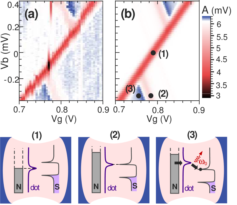
The self-energy corresponding to Eq.(84) is given in Ref.Bruhat:2016a . Using the above theory, Equation (67) gives the results of Fig.15b, which reproduce closely the data of Fig.15a. The line marked with the circle (1) corresponds to a resonance between the dot orbital and the Fermi level in the normal metal, whereas the circle (2) corresponds to a resonance between the dot level and a BCS peak in the superconducting reservoir. The effect is due to inelastic tunneling from the dot level to one BCS peak, which triggers the emission of a cavity photon, as represented in Fig.15.3
It is interesting to evaluate the performance of the device of Fig.15 as a photon emitter. In order to evaluate the emission rate of photons in the cavity by the quantum dot circuit, one needs to calculate the time evolution of the average number of cavity photons . By combining Eqs.(31), (32) and the top left Eq. of Fig.(5), one gets
| (88) |
with
| (89) |
the emission rate of photons inside the cavity by the nanocircuit. This rate can be simplified by eliminating fast oscillating terms which do not contribute significantly to photon emission. Using the linear response expression
| (90) |
with , we get
| (91) |
From Eq.(38) and (42), this can be expressed in terms of the experimental signals as:
| (92) |
The data of Fig.15 were measured with an average photon number in the cavity. The calibration of the experiment also gives and . The area with in Fig.15 corresponds to . From Eq.(92), this gives , which corresponds to an inelastic current of the order of . This current was not detectable in the experiment because of current noise.
V.4 Voltage-biased double quantum dot in a cavity
V.4.1 Probing out-of-equilibrium double dot populations with a microwave cavity
From Eq.(58), current transport in the double dot can modify the cavity signals by modifying the populations and of the bonding and antibonding states. The transport configuration can be tuned electrically through the double dot gate voltages and and source-drain bias voltage . Figure 16 presents results obtained with a carbon nanotube double quantum dot with a finite Coulomb interaction Viennot:2014a . As observed usually, the current through the double dot is finite only inside some triangles in the plane where the bonding or antibonding states are inside the transport window opened by the source-drain voltage (Fig.16a). The cavity signal is maximum along the line where is minimum (Figs.16b), and it takes a different value along the transport triangles, because the populations of or are modified by transport. In Fig.16c, this behavior is well reproduced by using Eq.(58), with and calculated with a master equation approach at lowest order in the light matter coupling () (see details in Ref.Viennot:2014a ). In the regime , this approach is sufficient to take into account Coulomb blockade, which essentially affects the structure of the nanocircuit state space and tunnel rates. The inclusion of Coulomb interactions in the Keldysh formalism is a more complex taskNg:1996 . Note that however, in the non-interacting case, the Keldysh approach also reproduces well the fact that is affected by current transport through a modification of (see Appendix VIII). Remarkably, the dc current through the double dot and the cavity signals are qualitatively different, since the cavity signals directly probe whereas the current is a more complex combination of , and the double dot parameters. Therefore, the simultaneous study of the two signals can again enable a more accurate characterization of the double dot parameters.
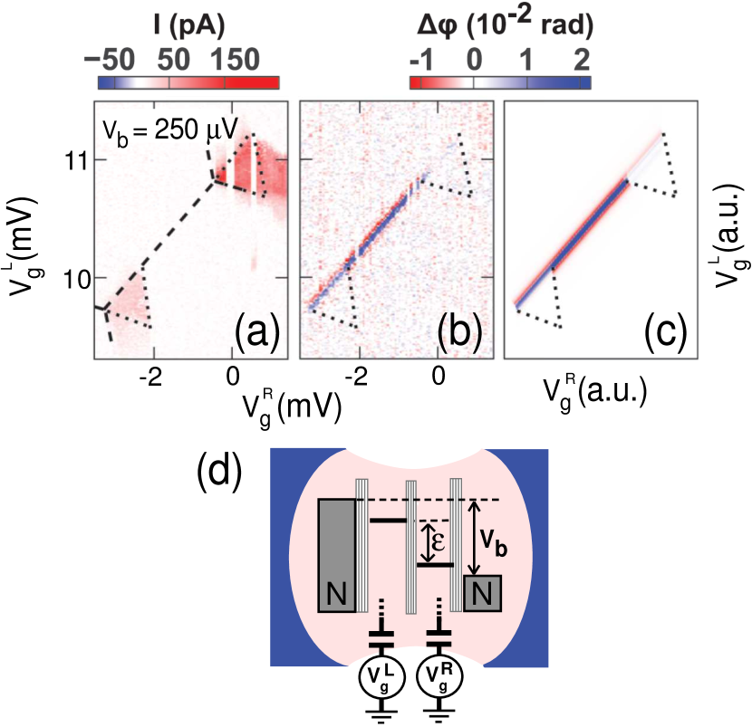
V.4.2 Photon emission below the lasing threshold
The splitting between the bonding and antibonding states of the double dot can become resonant with the cavity if is tuned properly. In this regime, it is possible to obtain photon emission due to the dc voltage bias. This phenomenon has been investigated in two dimensional electron gas structures and semiconducting nanowiresStockklauser:2015 ; Liu:2014 . In Ref.Stockklauser:2015 , the number of photons emitted by the cavity per unit time was measured as a function of the double dot detuning for a constant interdot detuning (see Figure 17a). For , two resonances appear in , for orbital detunings with . The resonance for is less pronounced than the resonance for because it requires that the electrons tunnel from the left reservoir to an antibonding state which has little extension on the left dot (see Figure 17.1). Figure 17b shows the measured value of versus , which can be tuned with gate voltages in two dimensional electron gas structures. As expected, vanishes for , because it is not possible to satisfy the resonant condition in this case. In this limit, the cavity shows a single resonance centered on (not shown). The light/matter coupling in this experiment can be estimated from the parameters , and , which corresponds to and . The data were interpreted with a master equation approach similar to the one of Ref.Viennot:2014a (see section V.4.1). In the out-of-equilibrium regime, the rate of photon emission in the cavity by the double dot is . This number is similar to the performances obtained with the normal metal/dot/superconductor bijunction of section V.3.
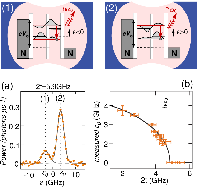
V.4.3 Photon emission above the lasing threshold
In principle, when a double dot with is resonant with a cavity (), it is possible to obtain a lasing effect, which corresponds to an emission of a coherent microwave radiation by the double dot, if PeiQing2011 ; PeiQing2012a ; PeiQing2013 ; Kulkarni:2014 ; Lambert:2015 ; Karlewski:2016 ; Marthaler:2015 ; Gullans:2016 . When , it is possible to reach the lasing regime by coupling several double quantum dots to the cavity. This was recently realized with two double dots made in InAs nanowiresLiu:2015a ; Liu:2015 . Figure 18 shows the in-phase and quadrature phase components I and Q of the output field of the cavity, measured when only one of the dots fulfills (panel (b)) or when the two dots satisfy (panel (c)). In the first case, the cavity photons show a thermal distribution, because the device is below the lasing threshold. In the second case, the ”ring” in the tomography reveals a coherent photonic emission, because the device is above the lasing threshold. An average photon number in the cavity is estimated in this last case. The rate of photon emission by the double dot can be estimated as , which is significantly larger than in Refs.Stockklauser:2015 ; Bruhat:2016a . Charge noise limits the maser linewidth. However, a linewidth narrowing by more than a factor of 10 can be obtained by using a microwave input tone that stabilizes the frequency of laser emission by triggering stimulated emissionLiu:2015 . This technique is known as injection locking in the field of conventional lasersStover . Note that in the lasing regime, the linear theory of section III.2 fails. We refer interested readers to Ref.Andre:2006 for a simple theoretical description of this limit. Interestingly, there is a close analogy between the lasing effect produced in a microwave cavity by an out-of-equilibrium quantum dot, and the one obtained with a Josephson superconducting transistor with a finite voltage biasAstafiev:2007 . In this second case, the lasing transition corresponds to a change in the number of Cooper pairs inside a superconducting island. In Ref.Astafiev:2007 , a photon emission rate inside the cavity has been obtained, which is comparable to the performance of Ref.Liu:2015 .
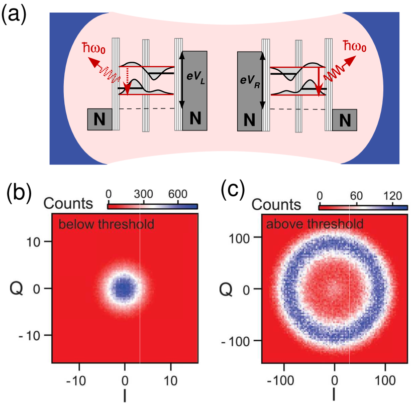
V.5 Characterizing exotic condensed matter systems with a microwave cavity
In the previous sections, we have considered relatively simple situations with nanocircuits made out of only one or two dots and fermionic reservoirs, in the non-interacting regime or in the Coulomb blockade regime. However, this section shows that the use of more complex circuits with possibly many body correlations enables one to study non-trivial quantum transport effects or condensed matter problems in a new way. Cavity photons appear as a new tool which can give qualitatively different information on exotic excitations in a nanocircuit, in comparison with traditional dc transport measurements. With mesoscopic QED devices, it is possible to measure simultaneously dc currents through the nanostructure and the microwave cavity response. The joint study of these two non-equivalent signals is particularly informative as we will see below.
V.5.1 Kondo quantum dots
The Kondo effect was observed experimentally since the 30’s [see for instance Ref.Franck:1961 ]. Although the resistivity of bulk metals is expected to decrease with temperature, for some metals containing a small amount of magnetic impurities an increase was observed below the Kondo temperature . Thirty years later, Kondo suggested that this behavior is due to spin-flip scattering processes between the itinerant electrons of the metal and the magnetic impuritiesKondo:1964 . These processes give birth to a Kondo cloud which screens the spins of the impurities and reduces the conductivity of the metal.
More recently, it was shown that quantum dots can also be used to study the Kondo effect if they are subject to a strong Coulomb interactionCronenwett:1998 ; Goldhaber:1998 ; Nygard:2000 . In this case, the spin-flip scattering processes give rise to an increase of the dot zero-bias conductance. This effect depends on the value of the charging energy to add a second electron in a dot level. If is large and that the dot orbital energy fulfills , there can only be a single electron in the dot orbital, whose electronic spin simulates a local magnetic impurity. Then, if the dot is coupled to normal metal contacts with a high enough tunnel rate , the local spin in the dot can fluctuate due to even order tunnel processes, which change the dot spin but not its charge. These processes involve intermediate virtual dot states with a different charge (dot orbital empty or doubly occupied), which are energetically forbidden but quantum mechanically allowed for a very short amount of time . Therefore, the Kondo effect should remain transparent to a microwave cavity which is only sensitive to charge fluctuations at frequencies . Importantly, this test requires that the cavity is mainly coupled to the dot level so that the cavity signals are set by the dot charge susceptibility. On the contrary, if the cavity modulates asymmetrically the potentials of the source and drain reservoirs, the cavity signals can reveal resonances similar to the Kondo conductance peak, as found experimentally in Refs.Delbecq:2011 ; Deng:2016
The charge susceptibility of a Kondo dot has been studied recently in a carbon nanotube quantum dot which is coupled to the cavity through the dot energy level onlyDesjardins:2017 . Both the Kondo regime and the Coulomb blockade regime have been studied with the same sample. In the Coulomb blockade regime, the conductance peaks through the dot are also visible in the cavity signals because they correspond to real charge fluctuations which are visible by cavity photons. However, in the Kondo regime, the low energy Kondo peaks are visible in the dot conductance but not in the cavity signals. Hence, the Kondo effect corresponds to conduction through essentially frozen charges in the dot (for a detector with a frequency cutoff ). This illustrates the decoupling of the spin and charge dynamics in the Kondo effect.
V.5.2 The Cooper pair splitter
The spatial separation of spin-entangled electrons from a Cooper pair is an interesting goal in the context of quantum computation and communication. In principle, a Cooper pair beam splitter (CPS) connected to a central superconducting contact and two outer normal metal (N) contacts could facilitate this processRecher:2001 . The spatial splitting of Cooper pairs has been demonstrated experimentally from an analysis of the CPS average currents, current noise, and current cross-correlations, in devices made out of a carbon nanotubeHofstetter:2009 ; Herrmann:2010 ; Hofstetter:2011 ; Schindele:2012 ; Herrmann:2012 ; Schindele:2015 or a semiconducting InAs quantum wireDas:2012 . However, new tools appear to be necessary to investigate further the Cooper pair splitting dynamics, and in particular its coherence, which has not been demonstrated experimentally so far in the N/dot/S/dot/N geometry. This coherence has two intimately related aspects: the coherence of Cooper pair injection and the conservation of spin entanglement. The first aspect is due to the fact that Cooper pair injection into the CPS is a coherent crossed Andreev process, which produces a coherent coupling between the initial and final states of the Cooper pair in the superconducting contact and the double dot. In this context, coupling the CPS to a microwave cavity would be very interesting because it would enable one to perform the spectroscopy of the CPS and identify anticrossings in the CPS spectrum, which are due to the coherence of the injection processCottet:2014 . Detecting the conservation of spin entanglement represents an even greater challenge. In principle, microwaves couple to transitions between the states of the CPS with matrix elements which keep signatures of the coherent superposition of spins states displayed by a singlet state. Therefore, a microwave cavity could help to characterize split singlet statesCottet:2012 . Interestingly, a supercurrent was recently observed in Josephson junction made out of two self-assembled quantum dots coupled in parallel to two superconducting contactsDeacon:2015 . The observation of a supercurrent necessarily implies a non-dissipative and thus coherent pair injection process. However, even in this case, the use of a microwave cavity would be very interesting to characterize further the device, i.e. perform its spectroscopy and check whether the coherent Cooper pair injection really goes together with a spin-entangled double dot state.
V.5.3 Majorana nanocircuits
Majorana quasiparticles are among the most intriguing excitations predicted in condensed matter physicsKitaev . By definition, the creation operator of a Majorana quasiparticle is self adjoint, i.e. . This property offers possibilities of non-abelian statisticsIvanov and topologically protected quantum computationNayak in condensed matter systems. It has been found that different types of hybrid electronic circuits could enclose Majorana quasiparticles. In particular, hybrid structures combining a semiconducting nanowire in contact with a superconductor raise a lot of attentionMourik ; Das ; DengDeng:2012 ; Churchill ; Albrecht ; Deng:2016b ; Zhang:2016 . It has been predicted that in some situations, a single pair of overlapping Majorana bound states could appear inside a semiconducting nanowire, with an overlap which can be switched off with an external magnetic field or a gate voltage, in order to obtain two isolated Majorana bound statesLutchyn ; Oreg . Recently, pairs of conductance peaks with a splitting oscillating and decaying with the magnetic field were observed, in striking agreement with these predictionsAlbrecht ; Deng:2016b . However, so far, mainly dc conductance measurements have been used, which reveal essentially the DOS of the nanowire. This gives only a very indirect access to the property . A microwave cavity could represent an interesting tool to test more directly this property since the self-adjoint property affects the structure of the light-matter coupling. Here, we will mainly focus on the proposal of Ref.Dartiailh:2016 , which considers a nanowire contacted to a superconducting contact and two normal metal tunnel probes (Figure 19a). In practice, it is possible to measure simultaneously from the cavity response, and the DOS of the nanowire by using the tunnel probes. The Keldysh theory was used to calculate these two quantities, by using a coarse grained description of the nanowire (see Eq.(67) and Figures 19b and c). To understand how a Majorana pair affects physical signals it is convenient to reexpress the degree of freedom associated to the Majorana pair by defining an ordinary fermion operator which fulfills . At low energies, in the subspace spanned by , one gets the nanocircuit Hamiltonian (23) with and (with the conventions of Eqs.(64) and (65), one has and ). This means that the Majorana pair corresponds to a fermionic state which can be split into two fully independent parts for . In the simplest situation, when the nanowire is driven to its topological phase, tends to zero, by showing or not an oscillatory behavior, depending on the length of the nanowire. The electron-hole conjugated pair appears in the DOS of the nanowire as a pair of resonances at and (see Figure 19b). However, no transition should be visible in the cavity signals at because from Eq.(66), the cavity photons cannot induce transitions between a pair of electron-hole conjugated states (see Figure 19c). Nevertheless, the light-Majorana coupling has physical consequences, since it can induce a step at in the signal. This feature is due to photo-assisted tunneling between the Majorana pair and the residual zero-energy DOS in the imperfect superconducting reservoir. It can be used to check that the low-energy doublet is well coupled to cavity photons, so that the absence of a cavity resonance at is not due to . Then, the simultaneous presence[absence] of the step at would represent a good indication that the low energy doublet in the nanowire results from the combination of a non-degenerate electron-hole pair, which is a natural precursor for a Majorana pair. Importantly, this information cannot be directly obtained from the DC current. Importantly, this protocol requires to measure simultaneously the cavity response and the dc current through the tunnel probes. Although the spectroscopic measurement described above is probably the most straightforward measurement to perform with a cavity, many other effects are expected by combining Majorana fermions and cavities. Hence, the direct electric coupling between Majorana bound states and cavity photons has raised a lot of attention recentlyTrif:2012 ; Schmidt:2013a ; Schmidt:2013b ; Cottet:2013 ; Dmytruk:2015 . The indirect coupling of Majorana fermions to cavities through a superconducting quantum bit also raises interest for quantum computation purposesVayrynen ; Hassler ; Hyart ; Muller ; Xue ; Pekker ; Ginossar ; Ohm ; Yavilberg ; Yavilberg2 .
VI Conclusion and perspectives
In this review, we have shown that a microwave cavity represents a powerful tool to investigate the properties and dynamics of electrons in a hybrid nanocircuit. In the linear-coupling regime, the microwave cavity gives an access to the charge susceptibility of the nanocircuit, which can be used to understand most Mesoscopic QED experiments realized so far. First, many different types of electronic degrees of freedom can be coupled coherently or strongly to cavity photons. In particular, we have reviewed several promising experiments where cavity photons are strongly or coherently coupled to the chargeMi:2017 ; bruhat:2017 ; Stockklauser:2017 or spinViennot:2015 of a double dot or Andreev statesJanvier:2015 in an atomic contact. The investigation of the coherent dynamics of these degrees of freedom now seems accessibleJanvier:2015 . Second microwave cavities give a new access to the tunneling dynamics of electrons between a dot and fermionic reservoirs. In equilibrium conditions, the charge relaxation dynamics caused by a fermionic reservoir can be studied with a high sensitivity. A first experiment seems consistent with a non-interacting theory which suggests the universality of the charge relaxation resistance in the adiabatic regimeBruhat:2016a . However, further study is required in the interacting case where a rich phenomenology is expected. In out-of equilibrium conditions, there exists several means to obtain photon emission, by using inelastic tunneling between a quantum dot and a reservoir with an energy-dependent DOSBruhat:2016a , or by using inelastic tunneling between two different quantum dotsStockklauser:2015 ; Liu:2014 ; Liu:2015a ; Liu:2015 . It was possible to obtain the lasing emission of a coherent photon field by coupling several voltage-biased double dots to a microwave cavityLiu:2015a . Finally, Mesoscopic QED represents a new tool to study exotic condensed matter states, as shown by a recent experiment for a quantum dot in the Kondo regimeDesjardins:2017 . Recent theory proposals also suggest to study split Cooper pairsCottet:2012 ; Cottet:2014 and Majorana bound states with a microwave cavityTrif:2012 ; Schmidt:2013a ; Schmidt:2013b ; Cottet:2013 ; Dmytruk:2015 ; Dartiailh:2016 .
One interesting feature of Mesoscopic QED is that many geometries can be realized thanks to the versatility of nanofabrication techniques. Furthermore, many different experimental protocols are possible thanks to the control on the nanocircuit dc bias and the microwave supply and detection. Therefore many situations can be investigated. There are many possible research directions in continuation of the works mentioned in this review:
Most of the experiments performed so far have been realized with a large number of photons, i.e. , such that a semiclassical description of the cavity response is sufficient to understand the measurements. The regime has been used very recently for the study of the strong nanocircuit/cavity coupling, in the stationnary regime where the cavity response versus the excitation frequency shows a characteristic splittingMi:2017 ; bruhat:2017 ; Stockklauser:2017 . Many other quantum phenomena are expected for , especially in the time domain, by analogy with Circuit QED experiments with superconducting quantum bits, and beyond if quantum transport to the reservoirs is involved. It is one of the main goals of Mesoscopic QED to explore this possibility.
The nonlinear regime, where multi-photon emission or absorption by the nanocircuit is possible, is a particularly interesting regimeGullans:2016 ; Leppakangas:2017 ; Oliver:2005 ; Jooya:2016 . This regime can be obtained by increasing the amplitude of the cavity microwave drive or the intensity of the light/matter interaction.
In this review, we have essentially discussed how to use a microwave cavity to characterize the properties of a nanocircuit. One could also study how to use a nanocircuit to prepare non-classical photonic states other than the coherent field already obtained through the lasing effect Schiro:2014 . For instance, squeezed cavity states can be prepared using a non-linear light/matter interactionCottet:2013 ; Mendes:2015 . In this context, cavity state tomography and photon statistics would represent important quantities to exploreXu:2013b . So far, the cavity state tomography was performed only in the presence of two double quantum dots in the lasing regimeLiu:2015a .
Placing several nanocircuits in a microwave cavity would enable one to study a large variety of effects which involve the interaction between nanocircuits mediated by cavity photons Contreras-Pulido:2013 ; Lambert ; Bergenfeldt:2013 ; Bergenfeldt:2014 ; Han:2015 . First experiments have already been realized with carbon nanotubes and grapheneDelbecq:2011 ; Deng:2015a ; Han:2016 .
One could go further in the hybridization of devices by coupling both a quantum dot circuit and a superconducting quantum bit to a microwave cavityBerg:2014 ; Feng:2012 . The use of the superconducting quantum bit could for instance give further access to the electronic dynamics in the nanocircuit.
Finally, it would be interesting to transpose Mesoscopic QED to other types of cavities. First, one could imagine to couple nanocircuits to teraherz cavities. This would give a photonic access to other energy scales such as the charging energy of a Coulomb blockaded quantum dot. Second, the behavior of quantum dot circuits coupled to optical cavities is discussed theoretically in Refs.Gudmundsson:2012 ; Jonasson:2012 ; Abdullah:2013 ; Abdullah:2014 ; Arnold:2014 ; Gudmundsson:2015b ; Gudmundsson:2016a ; Abdullah:2015 ; Gudmundsson: 2016b . The fabrication of such devices is extremely challenging, but this could reveal effects related to the polarization of light. With the coplanar cavities considered in this review, these effects are irrelevant because the microwave fields profile is set by the shape of the microwave cavity.
To conclude, mesoscopic QED experiments open a new avenue to investigate the light matter interaction under a different perspective. Many research directions are possible for the future development of this field.
Acknowledgements: We would like to thank François Mallet and Zaki Leghtas for fruitful discussions. This work was financed by the ERC Starting grant CirQys and the EU FP7 Project No. SE2ND[271554].
VII Appendix A: Nanocircuit charge susceptibility with the Keldysh formalism
In this appendix, we show how to predict the charge dynamics of a generic nanocircuit which encloses a nanoconductor, assuming that the coupling of the nanocircuit reservoirs to the cavity electric field can be disregarded. The nanoconductor can be decomposed into sites with an index or . For the sake of generality, we do not specify the Hamiltonian of the nanocircuit, which is expressed in terms of electronic creation and annihilation operators and for an electron with spin in site . In the semiclassical limit and in the framework of the resonant approximation of section III.2.1, one can use an Hamiltonian ac excitation term
| (93) |
to account for the semiclassical drive of the nanocircuit by cavity photons. In the Keldysh formalism, the dynamics of the nanocircuit can be described by using retarded, advanced, and lesser Greens functions with ()Jauho:1994 . These Green’s function have a matrix structure which encloses site subblocks whose structure depends on the problem considered. For instance, in the presence of superconductivity and a single spin quantization axis, one can use Green’s functions with the Nambu structure:
| (94) |
with
| (95) |
| (96) |
| (97) |
Above, one must calculate the statistical average using the full time-dependent Hamiltonian . Since , one can obtain the nanocircuit charge response by calculating . Below, we perform this calculation at first order in in order to obtain the linear charge susceptibility of the nanocircuit. The first order perturbation theory in gives
| (98) | ||||
with
| (99) |
Above, is the Green’s function solution of the problem for . Examples of expressions of are given in sections V.2 and V.3. The matrix is a diagonal matrix which corresponds to in the orbital block and is zero otherwise. The combination of Eqs.(98) and (99) gives
| (100) | ||||
From the Langreth theoremJauho:1994 one has
| (101) |
with
| (102) |
The lesser self energy of the discrete levels due to the presence of the reservoirs can be expressed by following standard Keldysh rules (see e.g. section V.2 and Ref.Bruhat:2016a for examples). By combining Eqs.(98) and (101), in the non-interacting case, one gets at first order in :
| (103) | ||||
with
| (104) |
One can identify the charge susceptibility of site in response to an excitation at site by comparing the equation
| (105) |
which is due to the definition of and the equation
| (106) |
which defines , with the average charge in dot . In Eq.(105), the term is due to the fact that the Greens functions are defined in the Nambu space in the particular case of Eq.(94). Using the cyclic invariance of the trace, one finds
| (107) | ||||
This leads to Eq.(67) of the main text with . Note that a similar derivation can be performed without using the Nambu space in the case of a problem without superconductivity, or by using an extended Nambu space if the nanocircuit includes non-homogeneous magnetic fields which induce spin rotations (see Ref.Dartiailh:2016 ). In this case, Eq.(67) still holds provided the matrix is defined consistently with the structure of the Green’s functions.
VIII Appendix B: Non-interacting double dot with the Keldysh non-interacting description
In this appendix, we show in the simple example of a non-interacting double quantum dot with two grounded normal metal reservoirs (see Fig.(7)) that the Keldysh approach of section V.1 leads to a nanocircuit charge susceptibility which can account simultaneously for internal transitions inside a nanoconductor, and tunneling between the nanoconductor and fermionic reservoirs. For simplicity, we disregard the spin degree of freedom. The double dot Hamiltonian is
| (108) | ||||
Above, is the creation operator for an electron in the dot . The operator creates an electron in the state of the normal metal reservoir attached to dot . We note the interdot hopping, and the tunnel hopping constant between dot and its reservoir. The double dot Green’s function can be defined as
| (109) |
Therefore, using the Keldysh description of nanocircuitsJauho:1994 , one gets from Eq. (108)
| (110) |
and
| (111) |
with and . Then, Eq.(67) gives
| (112) |
with
| (113) |
| (114) |
and
| (115) |
Above, is defined by Eq.(53) of the main text and one has
| (116) |
Equation (112) is similar to Eq.(15) of Ref.Cottet:2011 , obtained with a non-interacting diagrammatic approach. An inspection of the double dot Hamiltonian in the bonding/antibonding state basis reveals that corresponds to the transverse coupling between the bonding/antibonding transition and the cavity, whereas and correspond to the lever arms for the modulation of the bonding and antibonding energy levels by the cavity electric field. The complex expression (112) can be simplified in some particular limits to get a better physical insight. First, in the limit , one gets, from Eq.(112)
| (117) |
Hence, the terms in describe a quantum capacitance contribution which is due to the thermal equilibration of the bonding and antibonding states with the reservoirs. The term in describes another quantum capacitance contribution which is due to a transfer of electrons between the bonding and antibonding states of the double dot. This last term is maximally visible when the double dot has an occupation close to one electron, i.e. and . Second, in the limit and , one gets
| (118) |
which is similar to Eq.(58) of the main text, with and . These values of and stem from the fact that in the above lines, for simplicity, we have assumed that the normal metal reservoirs are grounded. Therefore, the population of the double dot states is thermal. It would be possible to generalize straightforwardly the above approach to the non-equilibrium case by using a term which would depend on the bias voltage. Note that in Ref.Dartiailh:2016 discussed in section V.5.3, it is also found that the charge susceptibility for a Majorana nanowire accounts for both tunneling to normal metal reservoirs (see Fig.19c, step highlighted with magenta dots) and transitions internal to the nanowire (see Fig.19c, resonance highlighted with black dots).
References
- (1) van Wees B J, van Houten H, Beenakker C W J, Williamson J G, Kouwenhoven L P, van der Marel D, and Foxon C T 1988 Phys. Rev. Lett. 60 848
- (2) Krans J M, Van Ruitenbeek J M, Fisun V V, Yanson I K and De Jongh L J 1995 Nature 375 767
- (3) Kouwenhoven L P, Marcus C M, McEuen P L, Tarucha S, Westervelt R M and Wingreen N S 1997, in Mesoscopic Electron Transport, edited by Sohn L L, Kouwenhoven L P, and Schön G (Kluwer Academic Publishers, Dordrecht/Boston/London), Series E: Applied Sciences 345 105
- (4) Shulman M D, Dial O E, Harvey S P, Bluhm H, Umansky V, Yacoby A 2012 Science 13, 202
- (5) Klein D L, Roth R, Lim A K L, Alivisatos A P, and McEuen P L, Nature (London) 389, 699 (1997).
- (6) Tans S J, Devoret M H, Dai H, Thess A, Smalley R E, Geeligs B L, and Dekker C, 1997 Nature 397, 474
- (7) De Franceschi S, van Dam J A, Bakkers E P A M, Feiner L F, Gurevich L, and Kouwenhoven L P 2003 Appl. Phys. Lett. 83, 344
- (8) Cottet A, Kontos T, Sahoo S, Man H T, Choi M-S, Belzig W, Bruder C, Morpurgo A F and Schönenberger C 2006 Semicond. Sci. Technol. 21 S78
- (9) Cottet A and Kontos T 2010 Phys. Rev. Lett. 105 160502
- (10) Recher P, Sukhorukov E V, and Loss D 2001 Phys. Rev. B 63 165314
- (11) Leijnse M and Flensberg K 2012 Semicond. Sci. Technol. 27, 124003
- (12) Kouwenhoven L P, Jauhar S, McCormick K, Dixon D, McEuen P L, Nazarov Yu V, van der Vaart N C and Foxon C T. 1994 Phys. Rev. B 50 2019
- (13) Oosterkamp T H, Fujisawa T, van der Wiel W G, Ishibashi K, Hijman R V, Tarucha S and Kouwenhoven L P 1998 Nature (London) 395 873.
- (14) Elzerman J M, De Franceschi S, Goldhaber-Gordon D, G. van der Wiel W and Kouwenhoven L P. 2000 J. Low Temp. Phys. 118 375
- (15) Schoelkopf R J, Wahlgren P, Kozhevnikov A A, Delsing P and Prober D E 1998 Science 280 1238
- (16) Fujisawa T and Hirayama Y 2000 Japanese Journal of Applied Physics 39, 2338
- (17) Cassidy M C, Dzurak A S, Clark R G, Petersson K D, Farrer I, Ritchie D A, and Smith C G 2007 Appl. Phys. Lett. 91, 222104
- (18) Reilly D J, Marcus C M, Hanson M P and Gossard A C 2007 Appl. Phys. Lett. 91, 162101
- (19) Ota T, Hayashi T, Muraki K, and Fujisawa T 2010 Appl. Phys. Lett. 96, 032104
- (20) Petersson K D, Smith C G, Anderson D, Atkinson P, Jones G A C, and Ritchie D A, Charge and spin state readout of a double quantum dot coupled to a resonator, Nano Lett. 10, 2789 (2010)
- (21) Chorley S J, Wabnig J, Penfold-Fitch Z V, Petersson K D, Frake J, Smith C G, and Buitelaar M R 2012, Phys. Rev. Lett. 108, 036802
- (22) Hayashi T, Fujisawa T, Cheong H D, Jeong Y H and Y. Hirayama Y 2003 Phys. Rev. Lett. 91 226804
- (23) Koppens F H L , Buizert C, Tielrooij K J, Vink I T, Nowack K C, Meunier T, Kouwenhoven L P and Vandersypen L M K 2006 Nature 442, 766
- (24) Nowack K C, Koppens F H L, Nazarov Yu V and Vandersypen L M.K 2007 Science 318 1430
- (25) Raimond J M, Brune M and Haroche S 2001 Rev. Mod. Phys. 73, 565
- (26) Wallraff A, Schuster D I, Blais A, Frunzio L, Huang R, Majer J, Kumar S, Girvin S M, Schoelkopf R J, 2004 Nature 431, 162
- (27) Paik H et Al. 2011 Phys. Rev. Lett. 107, 240501
- (28) Imamoglu A, Awschalom D D, Burkard G, DiVincenzo D P, Loss D and Sherwin M Small 1999 Phys. Rev. Lett. 83 4204
- (29) Burkard G and Imamoglu A 2006 Phys. Rev. B 74 041307(R)
- (30) Mi X, Cady J V, Zajac D M, Stehlik J, Edge L F and Petta J R 2017 Science 355 156
- (31) Bruhat L E, Cubaynes T, Viennot J J, Dartiailh M C, Desjardins M M, Cottet A and Kontos T, arXiv:1612.05214
- (32) Stockklauser A, Scarlino P, Koski J, Gasparinetti S, Kraglund Andersen C, Reichl C, Wegscheider W, Ihn T, Ensslin K, Wallraff A 2017 Phys. Rev. X 7, 011030
- (33) X. Mi, J. V. Cady, D. M. Zajac, J. Stehlik, L. F. Edge, J. R. Petta 2017 Appl. Phys. Lett. 110 043502
- (34) Viennot J J, Dartiailh M C, Cottet A and Kontos T 2015 Science 349 408
- (35) Janvier C, Tosi L, Bretheau L, Girit Ç Ö, Stern M, Bertet P, Joyez P, Vion D, Esteve D, Goffman M F, Pothier H and Urbina C 2015 Science 349 1199
- (36) Viennot J J, Delbecq M R, Dartiailh M C, Cottet A and Kontos T 2014 Phys. Rev. B 89 165404
- (37) Bruhat L E, Viennot J J, Dartiailh M C, Desjardins M M, Kontos T and Cottet A 2016 Phys. Rev. X 6 021014
- (38) Stockklauser A, Maisi V F, Basset J, Cujia K, Reichl C, Wegscheider W, Ihn T, Wallraff A and Ensslin K 2015 Phys. Rev. Lett. 115 046802
- (39) Liu Y Y, Petersson K D, Stehlik J, Taylor J M and Petta J R 2014 Phys. Rev. Lett. 113 036801
- (40) Liu Y-Y, Stehlik J, Eichler C, Gullans M J, Taylor J M and Petta J R 2015 Science 347 285
- (41) Liu Y-Y, Stehlik J, Gullans M J, Taylor J M and Petta J R 2015 Phys. Rev. A 92 053802
- (42) Cottet A, Kontos T and Levy Yeyati A 2012 Phys. Rev. Lett. 108 166803
- (43) Cottet A 2014 Phys. Rev. B 90 125139
- (44) Trif M and Tserkovnyak Y 2012 Phys. Rev. Lett. 109 257002
- (45) Schmidt T L, Nunnenkamp A and Bruder C 2013 Phys. Rev. Lett. 110 107006
- (46) Schmidt T L, Nunnenkamp A and Bruder C 2013 New J. Phys. 15 025043
- (47) Cottet A, Kontos T and Douçot B 2013 Phys. Rev. B 88 195415
- (48) Dmytruk O, Trif M and Simon P 2015 Phys. Rev. B 92 245432
- (49) Dartiailh M, Kontos T, Douçot M and Cottet A 2017 Phys. Rev. Lett. 118, 126803
- (50) Childress L, Sørensen A S and Lukin M D 2004 Phys. Rev. A 69 042302.
- (51) Frey T, Leek P J, Beck M, Ensslin K, Wallraff A and Ihn T 2011 Appl. Phys. Lett. 98 262105
- (52) Toida H, Nakajima T and Komiyama S 2012 Phys. Rev. Lett. 110 066802
- (53) Schmidt A R, Henry E, Lo C C, Wang Y T, Li H, Greenman L, Namaan O, Schenkel T, Whaley K B, Bokor J, Yablonovitch E and Siddiqi I 2014 J. Appl. Phys. 116 044503
- (54) Delbecq M R, Schmitt V, Parmentier F D, Roch N, Viennot J J , Fève G, Huard B, Mora C, Cottet A and Kontos T 2011 Phys. Rev. Lett. 107 256804
- (55) Ranjan V, Puebla-Hellmann G, Jung M, Hasler T, Nunnenkamp A, Muoth M, Hierold, Wallraff C and Schönenberger 2015 Nature Communications 6 7165
- (56) Petersson K D, McFaul L W, Schroer M D, Jung M, Taylor J M, Houck A A and Petta J R 2012 Nature 490, 380
- (57) Larsen T W, Petersson K D, Kuemmeth F, Jespersen T S, Krogstrup P, Nygard J and Marcus C M 2015 Phys. Rev. Lett. 115, 127001
- (58) de Lange G, van Heck B, Bruno A, van Woerkom D J, Geresdi A, Plissard S R, Bakkers E P A M, Akhmerov A R and DiCarlo L 2015 Phys. Rev. Lett. 115, 127002
- (59) Wang R, Deacon R S, Car D, Bakkers E P A M and Ishibashi K 2016 Appl. Phys. Lett. 108 203502
- (60) Zhang M-L, Wei D, Deng G-W, Li S-X, Li H-O, Cao G, Tu T, Xiao M, Guo G-C, Jiang H-W and Guo G-P 2014 Appl. Phys. Lett. 105 073510
- (61) Crisan A D, Datta S, Viennot J J, Delbecq M R, Cottet A and Kontos T 2016 Nature Communications 7, Article number: 10451
- (62) Waissman J, Honig M, Pecker S, Benyamini A, Hamo A and Ilani S 2013 Nature Nanotechnology 8, 569
- (63) Viennot J J, Palomo J and Kontos T 2014 Appl. Phys. Lett. 104 113108
- (64) Stehlik J, Liu Y-Y, Quintana C M, Eichler C, Hartke T R and Petta J R 2015 Phys. Rev. Applied 4 014018
- (65) Samkharadze N, Bruno A, Scarlino P, Zheng G, DiVincenzo D P, DiCarlo L and Vandersypen L M K 2016 Phys. Rev. Applied 5 044004
- (66) Köpke M and Weis J 2014 Physica C 506 143
- (67) Götz K J G, Blien S, Stiller P L, Vavra O, Mayer T, Huber T, Meier T N G, Kronseder M, Strunk Ch and Hüttel A K 2016 Nanotechnology 27 135202
- (68) Blien S, Götz K J G, Stiller P L, Mayer T, Huber T, Vavra O and Hüttel A K Phys. Status Solidi B, 253: 2385
- (69) Albert Fert, Rev. Mod. Phys. 80, 1517 (2008)
- (70) Cottet A, Kontos T, Belzig W, Schönenberger C and Bruder C 2006 Europhys. Lett. 74 320
- (71) Bertrand B, Flentje H, Takada S, Yamamoto M, Tarucha S, Ludwig A, Wieck A D, Bäuerle C, and Meunier T 2015 Phys. Rev. Lett. 115, 096801
- (72) M. D. Reed et al. 2016 Phys. Rev. Lett. 116, 110402
- (73) Martins F, Malinowski F K, Nissen P D, Barnes E, Fallahi S, Gardner G C, Manfra M J, Marcus C M, Kuemmeth F 2016 Phys. Rev. Lett. 116, 116801
- (74) D. Loss and D. P. DiVincenzo 1998 Phys. Rev. A 57, 120
- (75) Cohen-Tannoudji C, Dupont-Roc J, and Grynberg G 1997 Photons and Atoms: Introduction to Quantum Electrodynamics (New York: Wiley)
- (76) Blais A, Huang R-S, Wallraff A, Girvin S M and Schoelkopf R J 2004 Phys. Rev.A 69, 062320
- (77) Nigg s E, Paik H, Vlastakis B, Kirchmair G, Shankar S, Frunzio L, Devoret M H, Schoelkopf R J, and Girvin S M 2012 Phys. Rev. Lett. 108, 240502
- (78) Solgun F, Abraham D W, DiVincenzo D P, 2014, Phys. Rev. B 90, 134504
- (79) Vukics A, Grießer T, and Domokos P 2014 Phys. Rev. Lett. 112 073601
- (80) Cottet A, Kontos T and Douçot B 2015 Phys. Rev. B 91, 205417
- (81) Prange R E 1963 Phys. Rev. 131, 1083
- (82) In principle, in the presence of a cavity bosonic bath, one has to include the dissipation term of Eq.(29) in the Hamiltonian (12). Then, in order to obtain the photonic pseudo-potential picture, it is still sufficient to use the transformation (18) if there is a very weak spatial overlap between the nanocircuit and the modes of the bosonic bath. The exact form for Hamiltonian (28) is then slightly more complicated than what is indicated in the main text, because the transformation of the term by (18) leads to an extra coupling term between the electrons of the nanocircuit and the bosonic bath. One could expect an extra widening of the nanocircuit electronic levels by this term, with an order of magnitude . However, in the experiments, one has and is very small in comparison with the intrinsic damping of the dot levels by for instance by the metallic contacts. Therefore, equations (28) and (29) seem to be a good approximation for the description of cavity dissipation in the photonic pseudo-potential picture.
- (83) The drive term in can be obtained by treating explicitly the classical part of the bosonic bath mode excited by a microwave source.
- (84) Reulet B, Ramin M, Bouchiat H, and Mailly D 1995 Phys. Rev. Lett. 75, 124
- (85) Deblock R, Noat Y, Bouchiat H, Reulet B, and Mailly D 2000 Phys. Rev. Lett. 84, 5379
- (86) Walls D F Milburn G J 2008 Quantum Optics, 2nd edn. Springer, Berlin
- (87) Cottet A, Mora C and Kontos T 2011 Phys. Rev. B 83, 121311(R)
- (88) Thompson R J, Rempe G and Kimble H J 1992 Phys. Rev. Lett. 68, 1132
- (89) Brune M, Schmidt-Kaler F, Maali A,Dreyer J, Hagley E, Raimond J M and Haroche S 1996 Phys. Rev. Lett. 76, 1800
- (90) To define mathematically, we consider the resonant limit () with a negligible bare cavity linewidth (). Then, the threashold corresponds to having at , with given by Eq.(39) with .
- (91) Reithmaier J P, Sek G, Löffler A, Hofmann C, Kuhn S, Reitzenstein S,Keldysh L V, Kulakovskii V D, Reinecke T L and Forchel A 2004 Nature 432 197
- (92) Yoshie T, Scherer A,Hendrickson J, Khitrova G, Gibbs H M, Rupper G, Ell C,Shchekin O B and Deppe D G 2004 Nature 432 200
- (93) Frey T, Leek P J, Beck M, Blais A, Ihn T, Ensslin K and Wallraff A 2012 Phys. Rev. Lett. 108 046807
- (94) Schroer M D, Jung M, Petersson K D and Petta J R 2012 Phys. Rev. Lett. 109 166804
- (95) Frey T, Leek P J, Beck M, Faist J, Wallraff A, Ensslin K, Ihn T and Büttiker M 2012 Phys. Rev. B 86 115303
- (96) Delbecq M R, Bruhat L E, Viennot J J, Datta S, Cottet A and Kontos T 2013 Nature Communications 4 Article number: 1400
- (97) Toida H, Nakajima T and Komiyama S 2013 Phys. Rev. Lett. 110 066802
- (98) Basset J, Jarausch D-D, Stockklauser A, Frey T, Reichl C, Wegscheider W, Ihn T M, Ensslin K and Wallraff A 2013 Phys. Rev. B 88 125312
- (99) Basset J, Stockklauser A, Jarausch D-D , Frey T, Reichl C, Wegscheider W, Wallraff A, Ensslin K and Thomas Ihn 2014 Appl. Phys. Lett. 105 063105
- (100) Deng G-W, Wei D, Li S-X, Johansson J R, Kong W-C, Li H-O, Cao G, Xiao M, Guo G-C, Nori F, Jiang H-W and Guo G-P 2015 Nano Lett. 15 6620
- (101) Deng G-W, Wei D, Johansson J R, Zhang M-L, Li S-X, Li H-O, Cao G, Xiao M, Tu T, Guo G-C, J H-W, Nori F and Guo G-P 2015 Phys. Rev. Lett. 115 126804
- (102) Cottet A, Vion V, Joyez P, Aassime A, Esteve D, and Devoret M H 2002 Physica C 367, 197
- (103) Stehlik J, Liu Y-Y, Eichler C, Hartke T R, Mi X, Gullans M J, Taylor J M and Petta J R 2016 Double Quantum Dot Floquet Gain Medium, Phys. Rev. X 6 041027
- (104) K. D. Petersson, J. R. Petta, H. Lu, and A. C. Gossard, Phys. Rev. Lett. 105, 246804 (2010).
- (105) Freeman B M, Schoenfield J S, and Jiang H, Appl. Phys. Lett. 108, 253108 (2016)
- (106) Obata T, Takeda K, Kamioka J, Kodera T, Akhtar W M, Sawano K, Oda S, Shiraki Y, and Tarucha S, JPS Conf. Proc. 1, 012030 (2014)
- (107) Schuster D I et al. 2010 Phys. Rev. Lett. 105, 140501
- (108) Kubo Y et al. 2010 Phys. Rev. Lett. 105 140502
- (109) Zhu X et al. 2011 Nature 478 221
- (110) Tosi G, Mohiyaddin F A, Huebl H, and Morello A,AIP Advances 4, 087122 (2014).
- (111) Haikka P, Kubo Y, Bienfait A, Bertet P, Moelmer K 2017 Phys. Rev. A 95, 022306
- (112) Trif M, Golovach V N and Loss D 2008 Phys. Rev. B 77 045434
- (113) Xuedong H, Yu-xi L and Franco N 2012 Phys. Rev. B 86 035314
- (114) Kloeffel C, Trif M, Stano P and Loss D 2013 Phys. Rev. B 88 241405(R)
- (115) Beaudoin F, Lachance-Quirion D, Coish W A and Pioro-Ladrière M 2016 Nanotechnology 27, 464003
- (116) Khaetskii V and Nazarov 2000 Phys. Rev. B 61, 12639
- (117) Khaetskii V and Nazarov 2001 Phys. Rev. B 64, 125316
- (118) Erlingsson S I and Nazarov Yu V 2002 Phys. Rev. B 66, 155327
- (119) Tokura Y, van der Wiel W G, Obata T, and Tarucha S 2006 Phys. Rev. Lett. 96, 047202
- (120) Takeda K, Kamioka J, Otsuka T, Yoneda J, Nakajima T, Delbecq M R, Amaha S, Allison G, KoderaT, Oda S, Tarucha 2016 S Science Advances 2, e1600694
- (121) Ono K, Austing D G, Tokura Y and Tarucha S 2002 Science 297 1313
- (122) Pei-Qing J, Marthaler M, Shnirman A and Schön G 2012 Phys. Rev. Lett. 108 190506
- (123) Pei-Qing J, Jeske J, Greentree A D and Cole J H arXiv:1507.07198
- (124) Wang L, Tu T, Gong B and Guo G-C 2015 Phys. Rev. A 92 062346
- (125) Tian-Yi H; Guang-Wei D, Wei D and Guo-Ping G 2016 Chinese Physics Letters 33 047301
- (126) Russ M and Burkard G 2015 Phys. Rev. B 92 205412
- (127) Srinivasa V, Taylor J M and Tahan C 2016 Phys. Rev. B 94 205421
- (128) Russ M, Ginzel F and Burkard G 2016 Phys. Rev. B 94 165411
- (129) Sköldberg J, Löfwander T, Shumeiko V S and Fogelström M 2008 Phys. Rev. Lett. 101 087002
- (130) Koch J, Yu T M, Gambetta J, Houck A A, Schuster D I, Majer J, Blais A, Devoret M H, Girvin S M, and Schoelkopf.R J 2007 Phys. Rev. A 76, 04319
- (131) Burkard G and Petta J R 2016 Phys. Rev. B 94, 195305
- (132) Mi X, Peterfalvi C G, Burkard G, and Petta J R, arXiv:1704.06312
- (133) The resonance corresponding to line 1 in Fig S6e of the supplement of Ref.Deng:2015 has been used to extract the numbers shown in Table 1. The corresponding cavity parameters have been taken from Fig.S6a
- (134) The decoherence rate of the double dot was not given directly in Ref.Liu:2014 . Therefore, we have determined from the Figure S5a of its supplement the cooperativity , by using the equality with and the cavity transmission amplitude when the double dot is off-resonant and on-resonant respectivelyViennot:2015 . Using the numbers and given in the supplemental, one gets . Then, using , one gets
- (135) We use a definition of the cooperativity which is different from Ref.Mi:2017 , for consistency with the other Refs.
- (136) Chirla R, Manolescu A and Moca C P 2016 Phys. Rev. B 93 155110
- (137) Schuetz M J A, Giedke G, Vandersypen L M K and Cirac J I 2017, Phys. Rev. A 95, 052335
- (138) Canran X and Vavilov M G 2013 Phys. Rev. B 87 035429
- (139) Schiró M and Le Hur K 2014 Phys. Rev. B 89 195127
- (140) Härtle R and Kulkarni M 2015 Phys. Rev. B 91 245429
- (141) Wong C H, Vavilov M G 2017 Phys. Rev. A 95, 012325
- (142) Cirio M, De Liberato S, Lambert N and Nori F 2016 Phys. Rev. Lett. 116 113601
- (143) Dmytruk O, Trif M, Mora C and Simon P 2016 Phys. Rev. B 93 075425
- (144) Agarwalla B K, Kulkarni M, Mukamel S and Segal D 2016 Phys. Rev. B 94, 035434
- (145) Agarwalla B K , Kulkarni M, Mukamel S and Segal D 2016 Phys. Rev. B 94 121305
- (146) Gabelli J, Fève G, Berroir J M, Plaçais B, Cavanna A, Etienne B, Jin Y, and Glattli D C 2006 Science 313, 499
- (147) Nigg S, Lopez R, and Büttiker M 2006 Phys. Rev. Lett. 97, 206804 (2006).
- (148) Mora C and Le Hur K Nat. Physics 6, 697 (2010).
- (149) Hamamoto Y, Jonckheere T, Kato T, and Martin T 2010 Phys. Rev. B 81, 153305
- (150) Filippone M, Le Hur K and Mora C 2011 Phys. Rev. Lett. 107, 176601
- (151) Alomar M I, Lim J S and Sánchez D, Phys. Rev. B 94, 165425 (2016)
- (152) Büttiker M, Thomas H, and Prêtre A, Phys. Lett. A 180, 364 (1993)
- (153) Prêtre A, Thomas H, and Büttiker M, Phys. Rev. B 54, 8130 (1996).
- (154) Ng T-K 1996 Phys. Rev. Lett. 76, 487
- (155) Pei-Qing J, M Marthaler, J H. Cole, A Shnirman and G Schön 2011 Phys. Rev. B 84 035322
- (156) Pei-Qing J, M Marthaler, J H Cole, A Shnirman and G Schön 2012 Phys. Scr. T151 014032
- (157) J Jin, M Marthaler, Pei-Qing J, D Golubev and G Schön 2013 New Journal of Physics 15 025044
- (158) Kulkarni M, Cotlet O and Türeci H E 2014 Phys. Rev. B 90 125402
- (159) Lambert N, Nori F and Flindt C 2015 Phys. Rev. Lett. 115 216803
- (160) Karlewski C, Heimes A and Schön G 2016 Phys. Rev. B 93 045314
- (161) Marthaler M, Utsumi Y and Golubev D S 2015 Phys. Rev. B 91 184515
- (162) Gullans M, Stehlik J J, Liu Y-Y, Eichler C, Petta J R and Taylor J M 2016 Phys. Rev. Lett. 117, 056801
- (163) Stover H L and Steier W H 1966 Appl. Phys. Lett. 8 91
- (164) André S, Pei-Qing J, Brosco V, Cole J H, Alessandro Romito A, Shnirman A, Schön G, Phys. Rev. A 82, 053802 (2010)
- (165) André S, Brosco V, Marthaler M, Shnirman A, and Schön G 2009 Phys. Scr.T137, 014016
- (166) Astafiev O, Inomata K, Niskanen A O, Yamamoto T, Pashkin Yu A, Nakamura Y and Tsai J S, 2007 Nature 449 588
- (167) Franck J, Manchester F and, Martin D 1961 Proc. Roy. Soc. A263, 494
- (168) Kondo J. 1964 Prog. Theor. Phys. 32 37
- (169) Cronenwett S M, Oosterkamp T H, Kouwenhoven L P 1998 Science 281 540
- (170) Goldhaber-Gordon D, Shtrikman D H , Mahalu D et al. 1998 Nature 391, 156
- (171) Nygard J, Cobden D H and Lindelof P E Kondo 2000 Nature 408, 342
- (172) Deng G-W, Henriet L, Wei D, Li S-X, Li H-O, Cao G, Xiao M, Guo G-C, Schiro M, Le Hur K and Guo G-P arXiv:1509.06141
- (173) Desjardins M M, Viennot J J, Dartiailh M C, Bruhat L E, Delbecq M R, Lee M, Choi M-S, Cottet A and Kontos T 2017 Nature 545, 71
- (174) Hofstetter L, Csonka S, Nygård J and Schönenberger C Nature 461, 960 (2009)
- (175) Herrmann L G, Portier F, Roche P, Levy Yeyati A, Kontos T, and Strunk C, 2010 Phys. Rev. Lett. 104, 026801 (2010)
- (176) Hofstetter L, Csonka S, Baumgartner A, Fülöp G, d’Hollosy S, Nygård J and Schönenberger C, Phys. Rev. Lett. 107, 136801 (2011)
- (177) Schindele J, Baumgartner A and Schönenberger C 2012 Phys. Rev. Lett. 109, 157002
- (178) Herrmann L G, Burset P, Herrera W J, Portier F, Roche P, Strunk C, Levy Yeyati A, and Kontos T, arXiv:1205.1972
- (179) Schindele J, Baumgartner A, Maurand R, Weiss M, and Schönenberger C, Phys. Rev. B, 89, 045422 (2014).
- (180) Das A, Ronen Y, Heiblum M, Mahalu D, Kretinin A V and Shtrikman H, 2012 Nature Comm. 3, Article number: 1165
- (181) Deacon R S, Oiwa A, Sailer J,S. Baba S, Kanai Y, Shibata K, Hirakawa K and Tarucha S 2015 Nature Comm. 6, Article number: 7446
- (182) Kitaev A Y 2001 Phys.Usp. 44, 131
- (183) D. A. Ivanov Phys. Rev. Lett. 86, 268 (2001).
- (184) Nayak C, Simon S H, Stern A, Freedman M and Das Sarma S 2008 Rev. Mod. Phys. 80, 1083
- (185) Mourik V, Zuo K, Frolov S M, Plissard S R, Bakkers E P A M, and Kouwenhoven L P 2012 Science 336, 1003
- (186) Das A, Ronen Y, Most Y, Oreg Y, Heiblum M and Shtrikman 2012 Nat. Phys. 8, 887
- (187) Deng M T, Yu C L, Huang G Y, Larsson M, Caroff P, and Xu H Q 2012 Nano Letters 12, 6414
- (188) Churchill H O H, Fatemi V, Grove-Rasmussen K, Deng M T, Caroff P, Xu H Q and Marcus C M 2013 Phys. Rev. B 87, 241401
- (189) Albrecht S M, Higginbotham A P, Madsen M,Kuemmeth F, Jespersen T S, Nygård J, Krogstrup P and Marcus C M Nature 531, 206 (2016).
- (190) Deng M T, Vaitiekenas S, Hansen E B, Danon J., Leijnse M, Flensberg K, Nygård J, Krogstrup P and Marcus C M Science 354 1557 (2016)
- (191) Zhang H et al., arXiv:1603.04069
- (192) Lutchyn R M, Sau J D and Das Sarma S 2010 Phys. Rev. Lett. 105, 077001
- (193) Oreg Y, Refael G, and von Oppen F 2010 Phys. Rev. Lett. 105, 177002
- (194) Väyrynen J I, Rastelli G, Belzig W and Glazman L I 2015 Phys. Rev. B 92 134508
- (195) Hassler F, Akhmerov A R and Beenakker C W J 2011 New J. Phys. 13 095004
- (196) Hyart T, van Heck B, Fulga I C, Burrello M, Akhmerov A R and Beenakker C W J 2013 Phys. Rev. B 88 035121
- (197) Müller C, Bourassa J and Blais A 2013 Phys. Rev. B 88 235401
- (198) Xue Z-Y, Shao L B, Hu Y, Zhu S-L and Wang Z D 2013 Phys. Rev. A 88 024303
- (199) Pekker D, Hou C-Y, Manucharyan V E and Demler E 2013 Phys. Rev. Lett. 111 107007
- (200) Ginossar E and Grosfeld E 2014 Nat. Commun. 5 4772
- (201) Ohm C and Hassler F 2014 Phys. Rev. B 91 085406
- (202) Yavilberg K, Ginossar E and Grosfeld E 2015 Phys. Rev. B 92 075143
- (203) Yavilberg K, Ginossar E and Grosfeld E 2015 Phys. Rev. B 92 075143
- (204) Mendes U C and Mora C 2015 New J. Phys. 17 113014
- (205) Xu C and Vavilov M G 2013 Phys. Rev. B 88 195307
- (206) Contreras-Pulido L D, Emary C, Brandes T and Aguado R 2013 New J. Phys. 15 095008
- (207) Lambert N, Flindt C and Nori F 2013 Europhysics Letters 103 17005
- (208) Bergenfeldt C, Samuelsson P, Sothmann B, Flindt C and Büttiker M 2014 Phys. Rev. Lett. 112 076803
- (209) Bergenfeldt C and Samuelsson P 2013 Phys. Rev. B 87 195427
- (210) Ye H, Peng Y-W, Yu Z-Y, Zhang W and Liu Y-M 2015 Chinese Physics B 24 114202
- (211) van den Berg T L, Bergenfeldt C and Samuelsson P 2014 Phys. Rev. B 90 085416
- (212) Feng Z-B 2012 Phys. Rev. A 85 014302
- (213) Gudmundsson V, Jonasson O, Tang C-S, Goan H-S and Manolescu A 2012 Phys. Rev. B 85 075306
- (214) Jonasson O, Tang C-S , Goan H-S, Manolescu A and Gudmundsson V 2012 New J. Phys. 14 013036
- (215) Abdullah N R, Tang C-S, Manolescu A and Gudmundsson V 2013 The Journal of Physics: Condensed Matter 25 465302
- (216) Abdullah N R, Tang C-S, Manolescu A and Gudmundsson V 2014 Physica E 64 254
- (217) Arnold T, Tang C-S, Manolescu A and Gudmundsson V 2014 Physica E 60 170
- (218) Gudmundsson V, Sitek A, Lin P-y, Abdullah N R, Tang C-S and Manolescu A 2015 ACS Photonics 2 930
- (219) Gudmundsson V, Sitek A, Abdullah N R, Tang C-S and Manolescu A 2016 Annalen der Physik 528 394
- (220) Abdullah N R, Tang C-S, Manolescu A and Gudmundsson V 2016 ACS Photonics 3 249
- (221) Gudmundsson V, Jonsson T H, Bernodusson M L, Abdullah N R, Sitek A, Goan H-S, Tang C-S and Manolescu A 2017 Annalen der Physik 529, 1600177
- (222) Gudmundsson V, Abdullah N R, Sitek A, Goan H-S, Tang C-S and Manolescu A 2017 Phys. Rev. B 95, 195307
- (223) Jauho A P, Wingreen N S, and Meir Y 1994 Phys. Rev. B 50, 5528
- (224) Oliver W D, Yu Y, Lee J C, Berggren K K, Levitov L S, Orlando T P 2005 Science 310 1653
- (225) Jooya H Z, Reihani K, Chu, S-I 2016 Scientific Reports 6 37544
- (226) Leppäkangas J, Marthaler M, Hazra D, Jebari S, Johansson G, Hofheinz M, arXiv:1612.07098