Charge puddles in the bulk and on the surface of the topological insulator BiSbTeSe2 studied by scanning tunneling microscopy and optical spectroscopy
Abstract
The topological insulator BiSbTeSe2 corresponds to a compensated semiconductor in which strong Coulomb disorder gives rise to the formation of charge puddles, i.e., local accumulations of charge carriers, both in the bulk and on the surface. Bulk puddles are formed if the fluctuations of the Coulomb potential are as large as half of the band gap. The gapless surface, in contrast, is sensitive to small fluctuations but the potential is strongly suppressed due to the additional screening channel provided by metallic surface carriers. To study the quantitative relationship between the properties of bulk puddles and surface puddles, we performed infrared transmittance measurements as well as scanning tunneling microscopy measurements on the same sample of BiSbTeSe2, which is close to perfect compensation. At 5.5 K, we find surface potential fluctuations occurring on a length scale = nm with amplitude = meV which is much smaller than in the bulk, where optical measurements detect the formation of bulk puddles. In this nominally undoped compound, the value of is smaller than expected for pure screening by surface carriers, and we argue that this arises most likely from a cooperative effect of bulk screening and surface screening.
I Introduction
Three-dimensional topological insulators (TIs) are narrow-gap semiconductors with band inversion Ando13 . Many TIs such as Bi2Te3 and Bi2Se3 show metallic bulk conductivity due to defect-induced charge carrier densities of typically 1019 cm-3 Stordeur92 ; Analytis10 ; Ren10 ; LaForge10 ; Butch10 ; Eto10 ; Post13 . For investigations of the topological surface states, bulk-insulating samples are highly desirable. Bulk-insulating behavior was obtained in Bi2-xSbxTe3-ySey Taskin11 ; Ren11 by compensation of donors and acceptors Ando13 . For perfect compensation, donor density and acceptor density are equal, = , and electrons are transferred from donors to acceptors, suppressing the defect-induced charge density in both, conduction and valence bands. However, the randomly distributed ionized donors and acceptors give rise to Coulomb disorder, as discussed by Shklovskii and coworkers Shklovskii72 ; Skinner12 ; Skinner13 ; Chen13 . This yields strong band bending with potential fluctuations as large as , where denotes the band gap. Accordingly, the bands locally touch and cross the chemical potential Skinner12 , giving rise to local accumulations of charge carriers, the so-called puddles. These puddles can be viewed as regions which are either - or -doped, both occurring with equal probability for = . Puddles partially screen the large fluctuations of the Coulomb potential, and they “evaporate” with increasing temperature due to the additional screening contribution of thermally activated carriers Borgwardt16 . For bulk transport, puddles are assumed to explain the small activation energy observed in the resistivity Skinner12 , the coexistence of electron-type and hole-type carriers in compensated samples Rischau16 , and the gigantic negative magnetoresistance observed in TlBi0.15Sb0.85Te2 Breunig17 . However, the smoking gun for bulk puddles is a Drude-like feature in the optical conductivity which is suppressed on a temperature scale = given by the Coulomb interaction between neighboring dopants Borgwardt16 . Infrared transmittance data of BiSbTeSe2 yield = K Borgwardt16 .
It is important to understand in how far these strong fluctuations of the bulk Coulomb potential and the concomitant dramatic band bending affect the properties of the topological surface state. Even minute potential fluctuations cause spatial variations of the Fermi level within the gapless Dirac cone and thus create local accumulations of charge carriers at the surface, i.e., surface puddles. Compared to the bulk, the Dirac-like surface state thus gives rise to strongly enhanced screening Skinner13 . However, for a nominally undoped TI with the Dirac point at the Fermi level yielding a vanishing density of states, a simple linear response theory predicts the absence of screening. Nonlinear screening is, however, effective Skinner13 resulting in a reduced but finite amplitude of fluctuations of the surface potential. The corresponding spatial variations of the Fermi level are important for surface transport phenomena Skinner13 ; Xiong12a . This is well established in graphene with Coulomb disorder in the substrate Hwang07 ; Adam07 ; Martin08 ; Zhang09 ; Samaddar16 . Spatial variations of the surface density of states are measurable by scanning tunneling spectroscopy (STS) in the differential conductance . Indeed, STS data of doped Bi2Te3 and Bi2Se3 show a scatter in the Dirac point energy of meV Beidenkopf11 . Also, spatial fluctuations of have been reported for Bi1.5Sb0.5Te1.7Se1.3 Kim14 ; Ko16 and were argued to be the source of scattering of long-wavelength electrons, leading to pronounced quasi-particle interference Kim14 . However, a quantitative comparison of theoretical predictions and experimental results on the properties of both, surface puddles and bulk puddles measured in the same sample, e.g. by STS and optics, is still lacking.
The properties of bulk puddles and surface puddles – such as the carrier density in bulk puddles, the temperature scale of bulk puddle destruction, the length scale of surface puddle formation, and the fluctuations of the surface potential – are intimately linked to the degree of compensation and the Coulomb interaction between neighboring dopants,
| (1) |
with the elementary charge , the dielectric constant , and the defect density = Skinner13 ; Borgwardt16 . Both and are sample dependent. A systematic investigation of the relationship between bulk puddles and surface puddles as well as a quantitative comparison with theory therefore require to study bulk and surface properties on the same sample. The compound BiSbTeSe2 is ideally suited for this task since it is close to perfect compensation Borgwardt16 . Moreover, angle-resolved photo-electron spectroscopy (ARPES) has shown that the Dirac point is close to the Fermi level in BiSbTeSe2 Arakane12 ; Neupane12 , which enhances the sensitivity of the Fermi level to potential fluctuations. Here, we combine optical spectroscopy of BiSbTeSe2 to study bulk puddles and scanning tunneling microscopy (STM) and STS to investigate charge puddles at the surface of the same sample. At low temperatures, we indeed observe the coexistence of bulk puddles and surface puddles. In contrast to expectations, our results indicate that a quantitative description of the potential fluctuations on the surface, i.e. of surface puddles, requires to take into account the screening contribution of bulk carriers. This can be rationalized by comparing the relevant length scales.
II Experimental methods
The single crystals of BiSbTeSe2 used in the present study were grown from high-purity elements [Bi, Sb, and Te of 6N (99.9999%) and Se of 5N (99.999%) purities] by using a modified Bridgman method in a sealed quartz-glass tube as described in Ref. Ren11 . To facilitate the in-situ cleaving under UHV, the crystals were precut into platelets with a typical dimension of mm2 with the (111) plane as the wide face.
For STM measurements two different BiSbTeSe2 crystals were mounted with their backside to the STM sample holder by using silver-filled epoxy glue. On their topside a metal pin was attached normal to the crystal surface using the same glue. Cleaving was performed in the STM ultrahigh vacuum preparation chamber with mbar by moving the pin against a sharp edge, causing the crystal to cleave. The cleaved sample surface was moved into the STM bath cryostat within a few minutes, where the pressure was mbar. The two crystals displayed indistinguishable results, underlining the reproducibility of our experiments.
STM and STS were performed at 5.5 K and 77 K. Constant-height d/d point spectra as well as constant-current d/d maps were recorded, with being the bias voltage applied to the sample and the tunneling current. We refer to them as STS spectra and STS maps in the following. Both were measured with a lock-in amplifier using a modulation voltage of mV and a frequency of = Hz. Each STS spectrum was averaged at least three times. The STS maps and STM topographs were analyzed with the WSxM software Horcas03 .
Prior to the STM/STS investigations, we performed infrared transmittance measurements in the frequency range of 0.07 eV to about 0.9 eV using a Bruker IFS 66v/S Fourier-transform spectrometer equipped with a continuous-flow He cryostat. The data were recorded using unpolarized light with the electric field parallel to the cleavage plane. At 5 K, the samples are transparent up to about 250 meV, which corresponds to the band gap. The optical conductivity was calculated from the measured transmittance in combination with the reflectivity of a thick sample of BiSbTeSe2, as described in Ref. Borgwardt16 .
III Experimental results
III.1 Optical conductivity
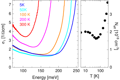
Charge carriers localized in puddles do not contribute directly to the DC conductivity, but for frequencies above a cutoff they cannot be distinguished from free carriers. For BiSbTeSe2, the estimated cutoff is very small, 0.01 meV Borgwardt16 . For frequencies much larger than , bulk puddles give rise to a weak Drude-like contribution to the optical conductivity Borgwardt16 . Such weak absorption features can be determined very well in transmittance measurements. The frequency range in which the sample is transparent then determines the experimentally accessible range of . The left panel of Fig. 1 shows of BiSbTeSe2 as obtained from a sample with a thickness of = m, where was determined from the observed Fabry-Perot interference fringes. For cm, the transmittance of this particular sample is below the noise level. Overall, the data agree very well with our previous results on BiSbTeSe2 Borgwardt16 . At 5 K, the steep increase at about 0.25 eV denotes the onset of excitations across the band gap . The broad feature at lower energy can be described in terms of a Drude peak. By fitting the spectra, we determined the spectral weight of this Drude peak which is a measure of the effective carrier density .
At high temperature, the Drude peak corresponds to thermally activated carriers which also contribute to the DC conductivity. The spectral weight of the activated Drude peak and thus drop steeply with decreasing temperature down to K, see right panel of Fig. 1. The presence of puddles is revealed by the non-monotonic temperature dependence of , i.e., the reincrease of below about 50 K.
By comparison with theory Borgwardt16 , the optical data allow us to estimate the carrier density in the bulk puddles, the defect density , and the degree of compensation . We find = = cm-3 using (see right panel of Fig. 1) and an estimate of the effective band mass of Borgwardt16 , where is the free electron mass. For an estimate of , we first consider perfect compensation, = . In this case, theory predicts = with the Coulomb interaction between neighbouring dopants defined in Eq. (1). With = Borgwardt16 and our experimental result of K, we find cm-3 which is equivalent to K. In the case of small deviations from perfect compensation such as = 0.98, theory predicts = . This yields cm-3 or K. Our experimental data shown in the right panel of Fig. 1 agree with the suppression of bulk puddles on a temperature scale of = K. We thus conclude that this sample of BiSbTeSe2 is close to perfect compensation and shows a defect density of = cm-3.
III.2 STM and STS data
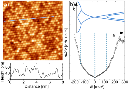
Large-scale STM topographs of the cleaved BiSbTeSe2 sample display flat terraces larger than 500 nm that are separated by steps of 10 Å height, or multiples thereof, consistent with a cleavage along the van der Waals gap between the quintuple layers of BiSbTeSe2 (compare also Kim14 ). The atomic-resolution STM topograph of Fig. 2(a) shows the hexagonal lattice of the surface atoms together with variations in the apparent atom heights. Through the height profile along the blue line in the topograph of Fig. 2(a), these height variations are quantified to be on the order of 50 pm. The variations are interpreted to result from the random arrangement of the chemical species in the mixed topmost Te/Se layer and in the mixed subsurface Bi/Sb layer. The chemical inhomogeneity is the origin of the apparent variation of the local electronic structure on the atomic scale. Similar observations were reported for the sister compound Bi1.5Sb0.5Te1.7Se1.3 Kim14 ; Ko16 . The cleaved surface is free of point defects (e.g. vacancies) and adsorbates.
Figure 2(b) displays a typical STS spectrum which shows the d/d signal versus energy = . The relation of features in the STS spectrum with the band structure as derived from ARPES Arakane12 ; Kim14 is visualized by the sketch in the inset. We find a dip in the d/d data that is attributed to the Dirac energy of the surface state. The Dirac point is located close to the Fermi energy, in agreement with ARPES results on BiSbTeSe2 Arakane12 . The top of the valence band is located at about -140 meV and the bottom of the conduction band at about 125 meV. Both are characterized by a slight change in the slope of the d/d signal. This implies a band gap of about 265 meV, in excellent agreement with the optical data of the same sample discussed above, see left panel of Fig. 1. In the energy range within the bulk band gap, the STS spectrum results exclusively from the surface state. The hallmark of an ideal Dirac cone is the linear dependence of the local density of states on energy, as observed for the unoccupied states at positive energy. Slight deviations from perfect linearity within the gap at negative energies reflect the well-known curvature of the topological surface state observed in ARPES on Bi2-xSbxTe3-ySey Arakane12 .
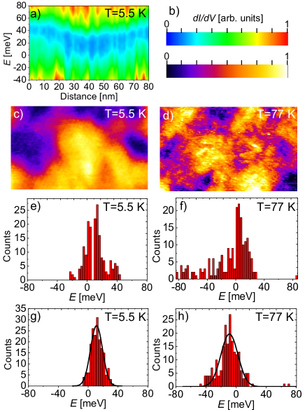
Local potential fluctuations due to ionized donors and acceptors lead to local energy shifts of the surface band structure and thus of the energy location of the Dirac point. Figure 3(a) represents these fluctuations through a sequence of 50 STS spectra taken along a line of 80 nm length. The d/d signal as a function of position and energy is visualized by a color scale ranging from blue to red as indicated in Fig. 3(b). The minimum in the d/d signal again corresponds to the Dirac point which smoothly shifts in energy with the lateral coordinate, whereby the characteristic length scale as given by the distance between minimum and maximum energy is of the order of = nm.
Figure 3(c) displays the corresponding d/d map taken near the Dirac energy at 5.5 K. The change in d/d [color code in Fig. 3(b)] corresponds to the energy shift of the surface band structure in line with the formation of surface puddles as shown in Fig. 3(a). Again a smooth shift of the surface band structure with respect to the Fermi level is visible, showing the same characteristic length scale of about = nm from minimum to maximum.
We also performed STM and STS measurements at 77 K to investigate the temperature dependence of the puddles, which is significant in the bulk, see Fig. 1. Figure 3(d) displays a d/d map taken at 77 K. It is more noisy but otherwise hardly distinguishable from the ones taken at 5.5 K. At first sight, this is remarkable since bulk puddles evaporate on a temperature scale of K, as discussed above.
To quantitatively characterize potential fluctuations, we took point spectra along lines of 80 nm to 100 nm length at 5 (7) different sample locations resulting in a total of 185 (200) spectra at 5.5 K (77 K). The results are shown in Figs. 3(e) and (f) for 5.5 K and 77 K, respectively. The energy of the dip found in each STS spectrum signifying the local Dirac point position = is extracted and collected in bins of 3 meV, where denotes the local electric potential. The potential fluctuations can be characterized quantitatively through the standard deviation = . At 5.5 K the average doping level of the sample is = = meV and the magnitude of the potential fluctuations is = 14 meV. At 77 K we find = meV and = meV. This representation of the data can be considered to be an upper bound for the potential fluctuations, as it assumes the absence of any tip-related effects on the data.
However, due to unavoidable occasional changes in the microscopic tip structure, e.g. by pick up of sample atoms, the tip density of states may change slightly between different locations at which the lines of spectra were taken. This may have an effect on the average measured doping level. To account for such possible parasitic effects related to the density of states of the tip, we subtracted the average Dirac energy of a line of spectra prior to their insertion into the histograms shown in Figs. 3(g) and (h) and centered these histograms at the respective global average. Applying this procedure, the standard deviation of the distribution measures a lower bound of the potential fluctuations. The magnitude of the potential fluctuations then is = meV at 5.5 K and = meV at 77 K. Here the distributions can be reasonably well fitted by Gaussians, which are shown in Figs. 3(g) and (h) as black lines.
Globally, it is fair to state that the samples of BiSbTeSe2 are close to perfect compensation with the average doping level close to zero, in excellent agreement with our optical data. Though our estimates of = meV at 5.5 K do not allow to precisely specify the magnitude of the potential fluctuations, we may safely conclude that is small, about an order of magnitude smaller than the bulk band gap. Despite our limited statistics and possible sources of systematic errors, we further conclude that is of similar magnitude at 5.5 K and 77 K. While the fluctuations of the bulk potential decrease with increasing temperature due to thermally activated carriers, we find no evidence for a decrease of the magnitude of surface potential fluctuations from 5.5 K to 77 K. With some reservation, our data rather suggest a slight increase.
IV Discussion
Using a self-consistent theory based on Thomas-Fermi screening by Dirac-like surface carriers, Skinner and Shklovskii Skinner13 calculated the amplitude of potential fluctuations = at the TI surface as well as the characteristic size of surface puddles caused by Coulomb disorder in the bulk for perfect compensation, = = . For nominally undoped TIs in which the Dirac point lies at the chemical potential, = , they find
| (2) |
with the effective fine structure constant
| (3) |
where = denotes the fine structure constant, the speed of light, and the Fermi velocity. The effective dielectric constant at the surface is given by = , where Borgwardt16 denotes the bulk dielectric constant. In Bi2-xSbxTe3-ySey, the dispersion of the topological surface state is not perfectly linear, giving rise to a variation of in the range of m/s Arakane12 ; Neupane12 ; Kim14 ; Ko16 . Altogether, we find = , significantly smaller than the value of 0.24 estimated by Skinner and Shklovskii for Bi2Se3 Skinner13 . With the optically determined defect density = cm-3, we find nm, in very good agreement with our STS result of nm.
Furthermore, Skinner and Shklovskii Skinner13 find
| (4) |
again for nominally undoped samples, = . With our experimental result of = K derived from the optical data, this yields a theoretical prediction of = meV, much larger than the value of meV observed in STS at 5.5 K. In the following we show that this inconsistency between theory and experiment can also be derived using only the STS data, without reference to our optical results. Theory predicts Skinner13
| (5) |
which depends only on and . The resulting prediction of = eVnm is an order of magnitude larger than the experimental STS result of eVnm at 5.5 K.
Equations (2) and (4) were derived for nominally undoped samples but are expected to apply as long as the chemical potential is smaller or at least not much larger than the potential fluctuations . For doped compounds with [cf. Eq. (4)], Skinner and Shklovskii find Skinner13
| (6) |
This limit of large is not applicable in BiSbTeSe2, as demonstrated by our STS results. In fact, Eq. (6) predicts an even larger value of than Eq. (4) for the experimentally determined parameters.
The calculations of Skinner et al. Skinner12 ; Skinner13 neglect the screening contribution of bulk puddles, i.e., they assume that all donors and acceptors are ionized. In other words, they assume that the formation of surface puddles is not affected by bulk puddles. This is valid for , where denotes the characteristic thickness of the near-surface layer in which bulk puddles are suppressed. For , the Coulomb disorder near the surface is screened by surface carriers with potential fluctuations (much) smaller than , preventing strong band bending and the formation of bulk puddles. Below, we will argue that in our system the assumption is not valid.
The size of bulk puddles – not to be confused with the thickness of the near-surface layer – was estimated by Shklovskii and coworkers by a simple scaling argument Skinner12 . It states that random fluctuations of the density of ionized defects in a volume give rise to an uncompensated charge and thus to a Coulomb potential . Bulk puddles are formed if these potential fluctuations are as large as , which leads to the estimate Skinner12
| (7) |
Using = 0.25 eV, = K, and = cm-3, we find nm. However, recent numerical results combined with a refined scaling argument by Bömerich et al. Boemerich17 predict much smaller values with for and
| (8) |
for . The same behavior but with a smaller prefactor is found for Boemerich17 . Under the assumption that the surface carriers screen like a perfect metal, i.e., large , Bömerich et al. predict in the range relevant to us, i.e., = . This corresponds to a thickness of the near-surface layer = nm which is even smaller than the measured characteristic size of surface puddles = nm. The assumption of perfectly metallic surfaces with a high chemical potential rather overestimates the value of in BiSbTeSe2. This result thus clearly suggests that the assumption is not valid anymore. Therefore, screening by bulk puddles may contribute to the surface properties, effectively reducing the amplitude of potential fluctuations on the surface. Altogether, these results indicate that surface puddles are not fully independent from bulk puddles and that a full quantitative description of the experimental data requires to consider a self-consistent description of both, surface and bulk properties.
Finally, we address the temperature dependence. The optical data show that bulk puddles "evaporate" with increasing temperature, the temperature scale is given by = K in our sample of BiSbTeSe2. In contrast, no strong change of the surface properties is observed in STS between 5.5 K and 77 K. Naively, this seems to suggest that surface puddles are independent of bulk carriers. However, the suppression of bulk puddles is due to the thermal activation of carriers in the bulk. Accordingly, the screening capability of the bulk is smoothly enhanced with increasing temperature. Bulk puddles vanish because the activated carriers reduce the potential fluctuations to a value smaller than . In other words, screening in the bulk at low temperatures is due to bulk puddles, but this role is taken over by activated carriers with increasing temperature. Therefore, it is very well possible that the temperature scale for the suppression of bulk puddles has little relevance to surface puddles.
V Summary and Conclusions
To address the relationship of surface puddles and bulk puddles, we performed infrared transmittance, STM, and STS investigations of the same sample of BiSbTeSe2. Measurements on the same sample are important since essential parameters such as the defect density and the degree of compensation are sample dependent. By in-situ cleaving, large-scale flat terraces of more than 500 nm were obtained. In agreement with previous results, STM and STS data show the hexagonal atomic structure and the chemical inhomogeneity of the Te/Se layers Kim14 ; Ko16 . Both optics and STS find a band gap of about 0.25 eV and show that BiSbTeSe2 is nearly undoped and close to perfect compensation.
Our data demonstrate the coexistence of bulk puddles and surface puddles at low temperatures. Both are caused by the Coulomb disorder originating from randomly distributed, ionized donors and acceptors. Although sharing the same origin, their properties are very different. Bulk puddles contribute to screening by neutralizing donors and acceptors, while the screening by surface puddles is based on the redistribution of highly mobile Dirac-like metallic carriers. Accordingly, the formation of bulk puddles requires that the potential fluctuations are as large as such that the bands touch the chemical potential. In contrast, surface puddles are formed for any finite variation of the surface potential since this will give rise to local shifts of the chemical potential for the gapless surface state. This major difference in energy scales explains their entirely different behavior as a function of temperature as well as the different length scales of surface puddles and bulk puddles. Bulk puddles "evaporate" at a temperature scale of when the screening contribution of activated carriers reduces the amplitude of potential fluctuations below . This temperature scale has little relevance to surface puddles since the total screening properties of the bulk evolve smoothly with temperature.
The quantitative analysis of our data allows us to address a possible interrelation of surface puddles and bulk puddles. Our optical data yield = , = cm-3, and a value of = K for the average Coulomb interaction between neighboring dopants. At 5.5 K, the STS measurements reveal an amplitude = meV of the surface potential fluctuations which occur on a length scale of = nm. The value of is much smaller than , which is the size of potential fluctuations in the bulk. We quantitatively compared the experimental results with the predictions of a self-consistent theory based on Thomas-Fermi screening by Dirac-like carriers Skinner13 which neglects the screening by bulk carriers. This is valid under the assumption , i.e., the length scale of surface puddles is much smaller than the thickness of the near-surface layer in which bulk puddles are suppressed. Our experimental result for is about an order of magnitude smaller than predicted by theory. In other words, screening by Dirac-like carriers is not sufficient to explain the small magnitude of surface potential fluctuations in nearly undoped BiSbTeSe2 with a small value of the chemical potential. However, numerical results in combination with a refined scaling argument reported recently Boemerich17 indicate that the assumption does not hold in BiSbTeSe2. We therefore conclude that surface puddles most probably are not fully independent from bulk puddles in BiSbTeSe2, i.e., the screening contribution of the bulk is relevant for surface properties at least as long as the surface chemical potential is close to the Dirac point. Further theoretical studies are called for to clarify whether quantitative agreement between experiment and theory indeed requires a self-consistent description of both, surface and bulk properties at the same time.
Acknowledgements.
Financial support of the Deutsche Forschungsgemeinschaft (DFG) through the Collaborative Research Center SFB 1238 (projects A04, B02, B06, and C02) is gratefully acknowledged. W.J. acknowledges financial support by the University of Cologne via the Advanced Postdoc Grant ’2D materials beyond graphene’ (PI: C. Busse).References
- (1) Y. Ando, Topological insulator materials, J. Phys. Soc. Jpn. 82, 102001 (2013).
- (2) M. Stordeur, K.K. Ketavong, A. Priemuth, H. Sobotta, and V. Riede, Optical and electrical investigations of n-type Bi2Se3 single crystals, phys. stat. sol. B 169, 505 (1992).
- (3) J.G. Analytis, R.D. McDonald, S.C. Riggs, J.-H. Chu, G.S. Boebinger, and I.R. Fisher, Two dimensional surface state in the quantum limit of a topological insulator, Nat. Phys. 6, 960 (2010).
- (4) Z. Ren, A.A. Taskin, S. Sasaki, K. Segawa, and Y. Ando, Large bulk resistivity and surface quantum oscillations in the topological insulator Bi2Te2Se, Phys. Rev. B 82, 241306(R) (2010).
- (5) A.D. LaForge, A. Frenzel, B.C. Pursley, T. Lin, X. Liu, J. Shi, and D.N. Basov, Optical characterization of Bi2Se3 in a magnetic field: Infrared evidence for magnetoelectric coupling in a topological insulator material, Phys. Rev. B 81, 125120 (2010).
- (6) N.P. Butch, K. Kirshenbaum, P. Syers, A.B. Sushkov, G.S. Jenkins, H.D. Drew, and J. Paglione, Strong surface scattering in ultrahigh-mobility Bi2Se3 topological insulator crystals, Phys. Rev. B 81, 241301(R) (2010).
- (7) K. Eto, Z. Ren, A.A. Taskin, K. Segawa, and Y. Ando, Angular-dependent oscillations of the magnetoresistance in Bi2Se3 due to the three-dimensional bulk Fermi surface, Phys. Rev. B 81, 195309 (2010).
- (8) K. W. Post, B.C. Chapler, L. He, X. Kou, K.L. Wang, and D.N. Basov, Thickness-dependent bulk electronic properties in Bi2Se3 thin films revealed by infrared spectroscopy, Phys. Rev. B 88, 075121 (2013).
- (9) A.A. Taskin, Z. Ren, S. Sasaki, K. Segawa, and Y. Ando, Observation of Dirac Holes and Electrons in a Topological Insulator, Phys. Rev. Lett. 107, 016801 (2011).
- (10) Z. Ren, A.A. Taskin, S. Sasaki, K. Segawa, and Y. Ando, Optimizing Bi2-xSbxTe3-ySey solid solutions to approach the intrinsic topological insulator regime, Phys. Rev. B 84, 165311 (2011).
- (11) B.I. Shklovskii and A.L. Efros, Completely Compensated Crystalline Semiconductor as a Model of an Amorphous Semiconductor, Sov. Phys. JETP 35, 610 (1972).
- (12) B. Skinner, T. Chen, and B.I. Shklovskii, Why Is the Bulk Resistivity of Topological Insulators So Small?, Phys. Rev. Lett. 109, 176801 (2012).
- (13) B. Skinner, T. Chen, and B.I. Shklovskii, Effects of Bulk Charged Impurities on the Bulk and Surface Transport in Three-Dimensional Topological Insulators, J. Exp. Theo. Phys. 117, 579 (2013).
- (14) T. Chen and B.I. Shklovskii, Anomalously small resistivity and thermopower of strongly compensated semiconductors and topological insulators, Phys. Rev. B 87, 165119 (2013).
- (15) N. Borgwardt, J. Lux, I. Vergara, Z. Wang, A.A. Taskin, K. Segawa, P.H.M. van Loosdrecht, Y. Ando, A. Rosch, and M. Grüninger, Self-organized charge puddles in a three-dimensional topological material, Phys. Rev. B 93, 245149 (2016).
- (16) C.W. Rischau, A. Ubaldini, E. Giannini, and C.J. van der Beek, Charge puddles in a completely compensated topological insulator, New J. Phys. 18, 073024 (2016).
- (17) O. Breunig, Z. Wang, A.A. Taskin, J. Lux, A. Rosch, and Y. Ando, Gigantic negative magnetoresistance in the bulk of a disordered topological insulator, Nat. Comm. 8, 15545 (2017).
- (18) J. Xiong, Y. Luo, Y.H. Khoo, S. Jia, R.J. Cava, and N.P. Ong, High-field Shubnikov – de Haas oscillations in the topological insulator Bi2Te2Se, Phys. Rev. B 86, 045314 (2012).
- (19) E. H. Hwang, S. Adam, and S. Das Sarma, Carrier Transport in Two-Dimensional Graphene Layers, Phys. Rev. Lett. 98, 186806 (2007).
- (20) S. Adam, E.H. Hwang, V.M. Galitski, and S. Das Sarma, A self-consistent theory for graphene transport, Proc. Nat. Acad. Sciences 104, 18392 (2007).
- (21) J. Martin, N. Akerman, G. Ulbricht, T. Lohmann, J.H. Smet, K. von Klitzing, and A. Yacoby, Observation of electron-hole puddles in graphene using a scanning single-electron transistor, Nat. Phys. 4, 144 (2008).
- (22) Y. Zhang, V.W. Brar, C. Girit, A. Zettl, and M.F. Crommie, Origin of spatial charge inhomogeneity in graphene, Nat. Phys. 5, 722 (2009).
- (23) S. Samaddar, I. Yudhistira, S. Adam, H. Courtois, and C. B. Winkelmann Charge Puddles in Graphene near the Dirac Point, Phys. Rev. Lett. 116, 126804 (2016).
- (24) H. Beidenkopf, P. Roushan, J. Seo, L. Gorman, I. Drozdov, Y. San Hor, R.J. Cava, and A. Yazdani, Spatial fluctuations of helical Dirac fermions on the surface of topological insulators, Nat. Phys. 7, 939 (2011).
- (25) S. Kim, S. Yoshizawa, Y. Ishida, K. Eto, K. Segawa, Y. Ando, S. Shin, and F. Komori, Robust Protection from Backscattering in the Topological Insulator Bi1.5Sb0.5Te1.7Se1.3, Phys. Rev. Lett. 112, 136802 (2014).
- (26) W. Ko, J. Park, I. Jeon, H.W. Kim, H. Kwon, Y. Oh, J.S. Kim, H. Suh, S.W. Hwang, and C. Chung, Local potential fluctuation of topological surface states in Bi1.5Sb0.5Te1.7Se1.3 observed by Landau level spectroscopy, Appl. Phys. Lett. 108, 083109 (2016).
- (27) T. Arakane, T. Sato, S. Souma, K. Kosaka, K. Nakayama, M. Komatsu, T. Takahashi, Z. Ren, K. Segawa, and Y. Ando, Tunable Dirac cone in the topological insulator Bi2-xSbxTe3-ySey, Nat. Comm. 3, 636 (2012).
- (28) M. Neupane, S.-Y. Xu, L.A. Wray, A. Petersen, R. Shankar, N. Alidoust, C. Liu, A. Fedorov, H. Ji, J.M. Allred, Y.S. Hor, T.-R. Chang, H.-T. Jeng, H. Lin, A. Bansil, R.J. Cava, and M.Z. Hasan, Topological surface states and Dirac point tuning in ternary topological insulators, Phys. Rev. B 85, 235406 (2012).
- (29) I. Horcas, R. Fernández, J.M. Gòmez-Rodríguez, J. Colchero, J. Gómez-Herrero, and A.M. Baro, WSXM: A software for scanning probe microscopy and a tool for nanotechnology, Surf. Sci. Instrum. 78, 013705 (2007).
- (30) T. Bömerich, J. Lux, Q.T. Feng, and A. Rosch, Length scale of puddle formation in compensation-doped semiconductors and topological insulators, Phys. Rev. B 96, 075204 (2017).