A Compact, Wide Field-of-View Gradient-index Lens Antenna for Millimeter-wave MIMO on Mobile Devices
Abstract
Lens-based beam-forming antennas offer a low-power, low-cost alternative to hybrid beamforming antenna arrays. They are ideally suited to millimeter-wave massive MIMO systems due to their native beam-space operation and angular selectivity and minimal dependence of high-speed data converters. We discuss the design of a compact and low-cost lens-based beam-forming antenna for small form-factor platforms such as small-cells and mobile devices in 5G wireless networks. We discuss a gradient-index design method and low-cost fabrication method based on perforated dielectrics. We discuss the need for high-contrast permittivity ranges to achieve wide scan angles which are essential for leveraging the full capability of massive MIMO systems (e.g., full stream capacity). Finally, we show that by using an appropriately designed perforated medium, gradient-index lenses with low minimum permittivity of can achieve a maximum beam-steering angle of degrees. We suggest that such an approach can enable practical low-loss, low-cost, and compact beam-steering lens antennas for millimeter-wave MIMO with wide beam-steering angles.
I Introduction
With the recently proposed FCC allocations for mobile wireless in the millimeter-wave (mmWave) bands, fifth generation (5G) wireless communications now seems inevitable. The move to mmWave brings with it the promise of wideband channels and almost unlimited spatial reuse [1]. However, to take advantage of this underutilized spectrum several significant challenges must be overcome. The dominant characteristic of millimeter-wave propagation is increased path loss. To realize a practical network under such constraints antenna arrays with high gain, beam-steering, and massive MIMO processing have been proposed [1, 2].
Traditional beam-steering approaches include digital base-band beamforming, analog RF/LO beamforming, and hybrid beamforming. While full digital beamforming offers the most flexibility it requires a data-converter and RF transceiver on every antenna element and is therefore prohibitive at 5G channel bandwidths[3]. Analog beamforming requires only a single data-converter and transceiver but only has one stream. Hybrid beamforming [4] has emerged as a compromise between digital and analog beamforming–in an element antenna array, baseband data-converters can be combined with RF phase shifters to provide high performance beam-steering, high-gain, and independent data streams. However, even hybrid beamforming has its limitations, namely cost, power and sensitivity to analog impairments due to finite-resolution, lossy mmWave phase shifters. In addition, signals from multiple angles of arrival (AoA) are incident upon all receive chains and so linearity requirements are increased.
One of the main motivations for moving to a large beam-steering array is to leverage the benefits of massive MIMO including high-gain and spatial multiplexing [5, 6]. Both are native beam-space concepts and so lens antennas, fundamentally beam-space devices, have been proposed as ideal apertures for mmWave MIMO [3]. The key advantage of lenses is inherent angle-, or beam-space selectivity. With a single RF chain a stream incident from any angle can be received with high gain. Reception of a specific beam from an AoA requires minimal processing and is realized in the completely passive lens medium. With RF chains, independent streams from angles of arrival can be received. Due to significant attenuation of multipath components, the typical number of paths (and therefore approximately the number of AoAs) in mmWave bands is [2] therefore a lens antenna with 2-8 transceivers and data-converters can capture all significant paths from any AoA up to the field of view (FOV) of the antenna. In [3] it was noted that an ideal lens antenna can achieve maximum MIMO capacity equal to times the channel capacity where is the number of spatial-multiplexed streams. A practical lens can approach this value only if every spatial stream emitted by the transmitter is intercepted by the receiver. Therefore, it is clear than any lens antenna for mmWave MIMO applications should have a large FOV to capture all streams.
In this paper we present a beam-forming lens antenna with wide FOV for use in small-form-factor platforms such as small-cells and even mobile devices. The lens is designed with transformation optics [7] and realized as a gradient index (GRIN) lens using stacked layers of perforated dielectric as we recently demonstrated in [8]. Because our process is based on photolithography, etching is parallel and therefore arbitrarily complex lenses can be fabricated for no additional cost and with negligible effect on fabrication time. From start to finish, each layer (wafer) of the GRIN lenses requires between 1-2 hours of etch time and since wafers are etched in batches, an entire lens can be etched in the same amount of time.
II Wide Field-of-view Lens Concept
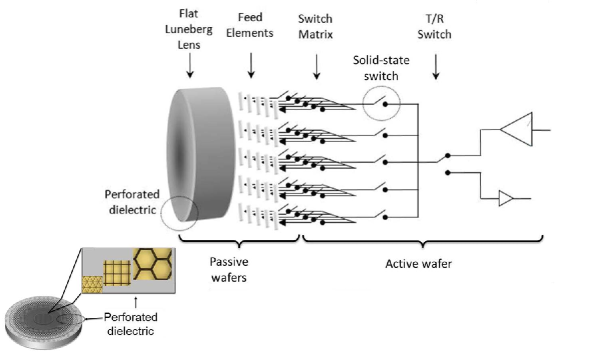
Figure 1 shows the lens antenna concept. The lens design is based on a flat Luneburg lens (FLL) fabricated with a stack of perforated silicon wafers. The FLL provides beam-steering by directing the RF signal to a particular feed element. The feed element () location dictates the beams (). The feed network is driven by an RF stream (single stream shown for clarity) through a matrix of solid-state switches. Importantly, mmWave switches are simpler to realize, lower loss, and require less power than variable phase shifters. Note that the switch matrix is only shown for concept clarity and is not the focus of this paper.
The FLL is designed with transformation optics [7]. Transformation optics (TO) is means of mapping a spatial distortion into a transformation of the material constitutive parameters (permittivity, and permeability, ). While a discussion of TO is beyond the scope of this report we summarize the approach: i) a coordinate transformation from physical space, () to virtual space () is defined, ii) the transformation is used to modify the permittivity and permeability tensors of an original design, and iii) the result is a spatial map of and which realize the functionality of the original structure in the physically transformed device.
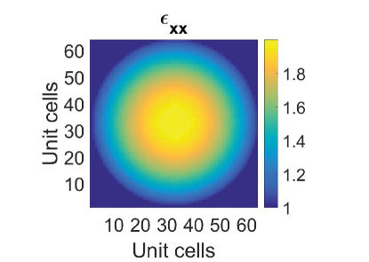
We now apply this process to the Luneburg lens which is a spherical lens whose permittivity varies from at the center of the lens to at the surface as shown in Fig. 2a.
| (1) |
The spherical lens is converted to a cylinder with a compression ratio, , which is introduced to compress the vertical, , axis:
| (2) | ||||
| (3) | ||||
| (4) |
Computing the Jacobian transfer matrix, , for the above coordinate transformation, we can compute the primed material:
| (5) |
which can be presented in terms of the original coordinates as shown in (6) and (7):
| (6) | ||||
| (7) |
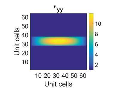
The resulting permittivity map is shown in Fig. 2b, from which we can see the length of the lens remains the same while the width is squeezed to . The permittivity distribution looks similar but is compressed. The electrical thickness must be much greater in the squeezed direction, which results in a maximum permittivity of . In our design shown in Fig. 2b, the maximum permittivity corresponds to at the center with a squeeze ratio of . The minimum permittivity is still at the edges.
The lens design is now fully prescribed in Fig 2b and we turn to the task of fabrication. By realizing the permittivity gradient with a perforated silicon dielectric, an effective permittivity can ideally range from 1 to 11.8. In the original work on perforated dielectrics [9] the medium was mechanically drilled to make circular voids on a square lattice (indicated with “Squ”, see Fig. 3c) and circular voids on a triangular lattice (indicated with “Tri”, see Fig. 3b) in a background dielectric. The effective permittivity of a perforated dielectric can be approximated as
| (8) |
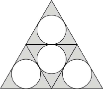
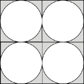
where is the relative permittivity of the background dielectric and is the filling factor equal to the ratio of the void area to the unit-cell area. For circular unit-cells on square and triangle lattices the minimum fill factor is equal to and , respectively. Recall that the permittivity map contains unit-cells with . We will show, later, that achieving a minimum permittivity close to is crucial for wide angle beam-steering of the lens. If the background permittivity is that of silicon, , the corresponding minimum effective permittivity of the “Squ” and “Tri” configurations are 3.3 ( of the background permittivity) and 2.0 ( of the background permittivity) respectively, which significantly limits the fabrication of many TO designs.
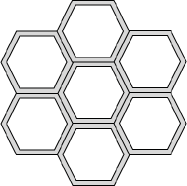
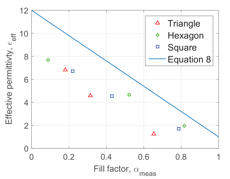
In order to approach we have proposed the use of gon voids on matched lattices and demonstrated their feasibility [8]. Figure 3a shows a hexagonal void on a hexagonal lattice. Theoretically the minimum permittivity can approach as the volume of unetched dielectric becomes asymptotically small. We have fabricated silicon wafers with permittivities as low as , or of the background permittivity. Figure 4 shows square, triangular, and hexagonal unit-cells on matched lattices. These structures were examined for robustness to manufacture and for their ability to exhibit a minimum permittivity. Features are exposed on an undoped silicon wafer with a diameter of mm and a thickness of m. Etching is performed with a Bosch process. The resulting permittivities are shown in Fig. 5 where the minimum permittivity value for the triangle structure is 1.25 which agrees with the the permittivity map constraints discussed above. Current Bosch etches exhibit significant undercut; fixing this problem will improve etch control.
![[Uncaptioned image]](/html/1708.05703/assets/x7.png)
III Wide-angle Beam-steering of Realistic Lenses
In this section we use Ansys HFSS to explore the performance limitations of such a beam-steering lens antenna under the above fabrication limitations. Our objective is to determine the importance of permittivity range and in particular minimum effective permittivity to achieve wide angle beam-steering.
If we constrain our fabrication to the three unit-cell structures shown in Fig. 3 we will be limited to minimum permittivities of , , and of the background permittivity for the “Squ”, “Tri”, and “Hex” configurations respectively. For a silicon background of , the minimum permittivities are , , and . Now truncating the permittivity map from Fig. 2b with these values we can count the percentage of unit-cells that are effected by the fabrication limitations as summarized in Table I. The background corresponds to base lens material of silicon (), and two potentially higher permittivities of and (corresponding to lens compression ratios of , and , respectively). Table I shows that for a silicon lens on a square lattice where the minimum fabricated permittivity is , of the unit cells in the idea design will have required permittivities below that of the fabrication limit. However, the same lens fabricated on a hexagonal lattice can realize a minimum fabricated permittivity of , resulting in only of prescribed cells being below the minimum fabrication limit. Lenses fabricated with a fewer number of prescribed cells below the fabrication limit will more faithfully realize the desired lens response. Table I shows that unit-cell structure while not thickness is the more important consideration for realizing the designed permittivity map.
| Background | Square lattice () | Triangle lattice (0.17) | Hexagon lattice (0.10) |
| (Si) | 12.29 | 5 | 2.02 |
| 12.7 | 5.164 | 1.844 | |
| 12.67 | 5.16 | 1.84 |
Figure 6 shows half of the final lens used for full-wave electromagnetic simulations. It is a rotational extrusion of the truncated permittivity maps. The lens is comprised of a array of unit-cells of size . The lens diameter is equal to where is mm, the free-space wavelength at . The associated thickness is mm. The focal point is mm which is almost identical to that of the typical Luneburg lens.
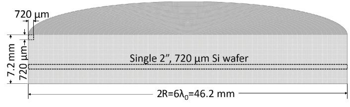
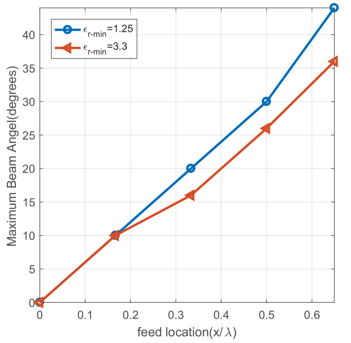
Figure 7 shows the maximum beam steering angle versus feed location for the silicon lens fabricated with “Squ” and “Hex” unit-cell configurations with minimum permittivity of and , respectively. At shallow scan angles the two lenses perform identically because the majority of the energy propagates throughout the center of the lens where permittivity is much higher than . However, as beam scan angle increases the “Hex” unit-cell with outperforms the “Squ” unit-cell. This is because as scan angle increases the edge of the lens plays a more prominent role in beam-steering and the edge of the lens contains the lower permittivity unit-cells.
IV Conclusion
In this paper, we present a way to design lens antennas by transformation optics. We have shown that by using an gon void on a matched lattice we can achieve a minimum permittivity of which yields a maximum beam-steering angle of degrees. This technology is a promising candidate for enabling practical low-loss, low-cost and compact beam-steering lens antennas for mmWave MIMO with wide beam-steering angles.
References
- [1] S. Hur, T. Kim, D. J. Love, J. V. Krogmeier, T. A. Thomas, and A. Ghosh, “Millimeter wave beamforming for wireless backhaul and access in small cell networks,” IEEE Transactions on Communications, vol. 61, no. 10, pp. 4391–4403, October 2013.
- [2] T. S. Rappaport, S. Sun, R. Mayzus, H. Zhao, Y. Azar, K. Wang, G. N. Wong, J. K. Schulz, M. Samimi, and F. Gutierrez, “Millimeter wave mobile communications for 5g cellular: It will work!” IEEE Access, vol. 1, pp. 335–349, 2013.
- [3] Y. Zeng and R. Zhang, “Millimeter wave mimo with lens antenna array: A new path division multiplexing paradigm,” IEEE Transactions on Communications, vol. 64, no. 4, pp. 1557–1571, April 2016.
- [4] A. Alkhateeb, J. Mo, N. Gonzalez-Prelcic, and R. W. Heath, “Mimo precoding and combining solutions for millimeter-wave systems,” IEEE Communications Magazine, vol. 52, no. 12, pp. 122–131, December 2014.
- [5] J. Hogan and A. Sayeed, “Beam selection for performance-complexity optimization in high-dimensional mimo systems,” in 2016 Annual Conference on Information Science and Systems (CISS), March 2016, pp. 337–342.
- [6] E. G. Larsson, O. Edfors, F. Tufvesson, and T. L. Marzetta, “Massive mimo for next generation wireless systems,” IEEE Communications Magazine, vol. 52, no. 2, pp. 186–195, February 2014.
- [7] D. H. Kwon and D. H. Werner, “Transformation electromagnetics: An overview of the theory and applications,” IEEE Antennas and Propagation Magazine, vol. 52, no. 1, pp. 24–46, Feb 2010.
- [8] N. Garcia, W. Bai, T. Twahirwa, D. Connelly, and J. Chisum, “Silicon micromachined high-contrast artificial dielectrics for millimeter-wave transformation optics antennas,” in to be presented at the 2017 IEEE International Symposium on Antennas and Propagation (APSURSI), July 2017.
- [9] A. Petosa and A. Ittipiboon, “Design and performance of a perforated dielectric fresnel lens,” IEE Proceedings - Microwaves, Antennas and Propagation, vol. 141, no. 5, pp. 309–, Oct 1994.