Emergence of Topological Nodal Lines and Type II Weyl Nodes in Strong Spin–Orbit Coupling System InNbX2(X=S,Se)
Abstract
Using first–principles density functional calculations, we systematically investigate electronic structures and topological properties of InNbX2 (X=S, Se). In the absence of spin–orbit coupling (SOC), both compounds show nodal lines protected by mirror symmetry. Including SOC, the Dirac rings in InNbS2 split into two Weyl rings. This unique property is distinguished from other dicovered nodal line materials which normally requires the absence of SOC. On the other hand, SOC breaks the nodal lines in InNbSe2 and the compound becomes a type II Weyl semimetal with 12 Weyl points in the Brillouin Zone. Using a supercell slab calculation we study the dispersion of Fermi arcs surface states in InNbSe2, we also utilize a coherent potential approximation to probe their tolernace to the surface disorder effects. The quasi two–dimensionality and the absence of toxic elements makes these two compounds an ideal experimental platform for investigating novel properties of topological semimetals.
I I. Introduction
In the past few years, topological semimetals, such as Weyl semimetals (WSM) Weyl-1 ; Weyl-2 , Dirac semimetals (DSM) DSM-1 ; nagaosa ; zhang ; Na3Bi ; Cd3As2 ; Cava-BaAgBi ; BaAgBi and Nodal Line semimetals (NLS)NSL-1 ; NSL-2 ; NSL-3 ; NSL-4 , have received tremendous research interest. In a Weyl semimetal, the electrons around Weyl points, which are the crossing points of two non–degenerate linearly dispersing energy bands, behave exactly like Weyl fermionsWeyl-1 ; Weyl-2 . With definite chirality, each Weyl point can be considered as a topologically protected charge, thus extending classification of topological phases of matter beyond insulatorsWeyl-1 ; Weyl-2 . Weyl points are extremely robust against weak perturbations and can only be annihilated when pairs of Weyl points with opposite topological charge meet with each other. Then the system opens a gap evolving into either a normal insulator or an Axion insulatorWeyl-1 ; axion .
One of the most remarkable properties of WSMs is the existence of topological surface states in a form of Fermi arcsWeyl-1 . This serves as an unambiguous evidence to identify this state of matter. A great number of other exotic phenomena has also been proposed for WSMs: a highly anisotropic negative magnetoresistance related to chiral anomaly effectChiral-1 ; Chiral-2 , a topological responseWeyl-response , unusual non–local transport propertiesnon-local , novel quantum oscillations from Fermi arcsQuantum-oscillations , etc.
A further classification here has been given to distinguish WSMs whose bulk Fermi surfaces shrink to Weyl points (called type I), or to exotic hyperboloid surfaces (called type II), where the cones are titled and induce a finite density of states at the nodal pointWTe2 . Due to the tilted nature of the nodes, the low energy excitations break Lorentz invariance, cause absence of the chiral anomaly at certain magnetic–field angles, magnetic breakdown and novel Klein tunneling WTe2 ; Type-II-2 .
There has been a great progress in searching for signatures of WSMs in real materials. Starting from the original proposal on pyrochlore iridates Weyl-1 , several systems, such, e.g., as HgCr2Se4 HgCr2Se4 , TaAsTaAs ; TaAs-hasan , WTe2WTe2 , NbPS2 , TaPS3 , NbAsS4 , MoTe28-exp-MoTe2 , MoP2, WP2S6 , LaAlGeS7 , etc. have been predicted to exhibit WSM behavior. A large amount of recent experimental work has been devoted to study properties of TaAs family S2 ; S3 ; S4 ; TaAs-exp-1 ; TaAs-exp-2 ; TaAs-exp-3 ; TaAs-exp-5 . In many of the proposed materials, however, the Weyl points do not exactly cross but only close to the Fermi level, and, in addition, there also are trivial Fermi states. The contribution from these trivial states significantly complicates the analysis of topological surface states and their novel transport behavior.
In addition to WSMs, a three–dimensional (3D) DSM DSM-1 ; nagaosa ; zhang ; Na3Bi ; Cd3As2 ; Cava-BaAgBi ; BaAgBi has also been proposed. The Dirac points in DSM are four–fold degenerate, and can be viewed as a merge of two Weyl fermions with opposite chirality in the Brillouin zone (BZ). The Dirac points usually require a protection by time reversal, inversion and additional crystal symmetry nagaosa ; zhang ; Na3Bi ; Cd3As2 .
Different from WSMs and DSMs which have finite numbers of band touching points in the BZ, a third topological semimetal, NLS has a whole crossing line in momentum spaceNSL-1 ; NSL-2 ; NSL-3 ; NSL-4 . Same as 3D DSM, NLS also needs crystal symmetry to stabilize its band crossing line zhang ; fuliang . The most exotic property of NLS is its two dimensional (2D) drumhead–like surface stateNSL-1 ; NSL-2 ; NSL-3 ; NSL-4 ; CaP3 ; BaSn2 ; CaTe ; NSL-mat-3 ; NSL-mat-4 ; NSL-mat-5 ; TlTaSe2 ; PbTaSe2 ; Ca3P2 . It has been speculated that this special state may realize high–temperature superconductivity NSL-app-1 ; NSL-app-2 .
Several materials have been predicted to be topological NLSs NSL-1 ; NSL-2 ; NSL-3 ; NSL-4 ; CaP3 ; BaSn2 ; CaTe ; NSL-mat-3 ; NSL-mat-4 ; NSL-mat-5 ; TlTaSe2 ; PbTaSe2 ; Ca3P2 . However, most of these predictions are based on calculations without spin–orbit coupling (SOC) NSL-2 ; NSL-3 ; NSL-4 ; CaP3 ; BaSn2 ; CaTe ; NSL-mat-3 ; NSL-mat-4 ; NSL-mat-5 ; Ca3P2 , inclusion of which leads normally to gapping out the nodal line NSL-2 ; NSL-3 ; NSL-4 ; CaP3 ; BaSn2 ; CaTe ; NSL-mat-3 ; NSL-mat-4 ; NSL-mat-5 ; Ca3P2 . Only in a few systems, this was found to be not the case, where TlTaSe2 and PbTaSe2 are predicted to remain NLS behavior in calculations with SOC TlTaSe2 ; PbTaSe2 .
Formally, topological semimetals exist only for 3D systems. However, quasi–2D layered materials that are easier to cleave and study their surface electronic structures are more favorable from the experimental perspective. Also, toxic elements like As, P, Tl and Hg found in many of the discovered materials create additional complications. Thus, searching for new topological systems and finding ways to remove the effects of trivial states meanwhile preserving contributions from topological Fermi arcs, are important problems of this emergent field of condensed matter physics.
In this work, we use first–principles calculations based on density functional theory (DFT) in its generalized gradient approximation (GGA) GGA to predict that InNbS2 and InNbSe2 show nodal lines and Weyl semimetal behavior, respectively. Without considering SOC, both of them are NLSs, and the band crossing lines are formed by four–fold degenerate Dirac points. The nodal lines, which are located around H point in the plane (i.e. L-H-A plane) in the BZ, are protected by the mirror symmetry. Including SOC, the four–fold degenerate nodal line in InNbS2 splits into two Weyl type nodal lines which are again protected by the mirror symmetry. On the other hand, the SOC changes InNbSe2 to a type II WSM for which we predict the Fermi arc surface states to appear on a easily cleavable (001) Indium terminated surface. Using a combination of DFT with Coherent Potential Approximation (CPA) we also simulate the effects of surface disorder to study the robustness of the Fermi arcs in this system. Our theoretical work shows that the InNbS2 and InNbSe2 are very promising materials for studying NLSs and WSMs, respectively.
II II. Crystal Structure
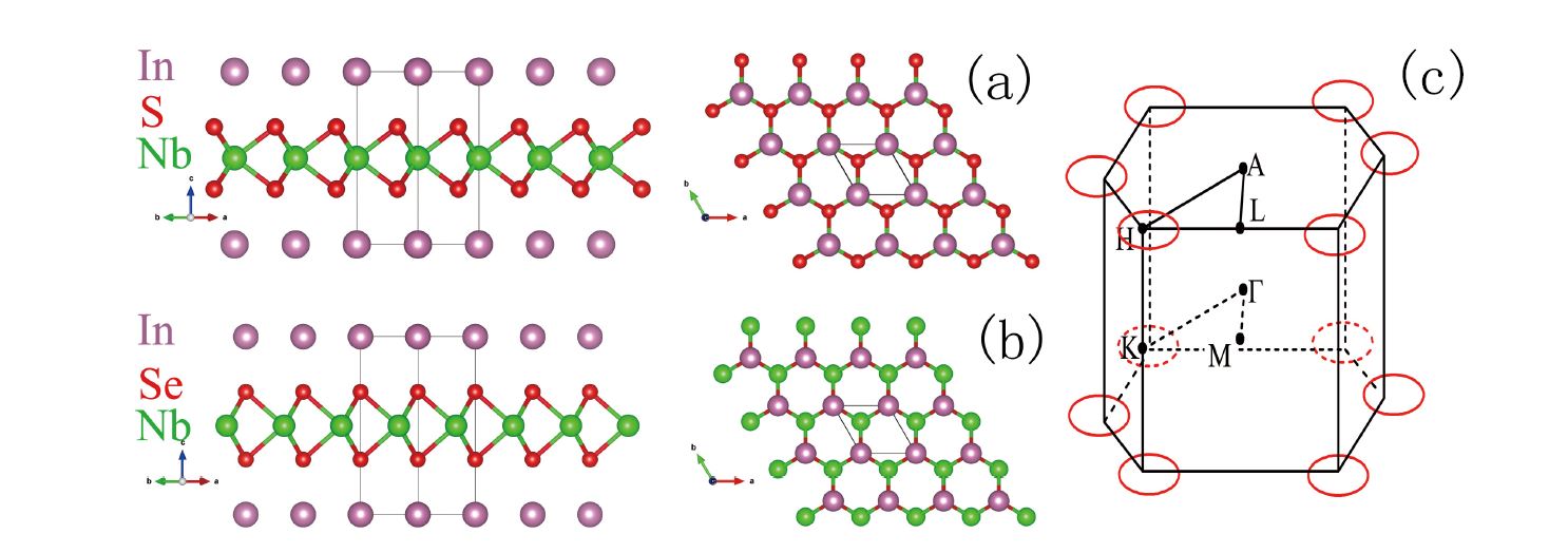
The crystal structures of InNbX2 (X=S, Se) belong to space group (NO. 187) which is non–centrosymmetriccry-1 ; cry-2 ; cry-3 . The In layer is intercalated between two niobium dichalcogenides layers. As shown in Fig. 1(a) and Fig. 1(b), the mirror plane is located at In layer or Nb layer. As discussed later in our work, this mirror plane plays a key role in protecting the nodal line. As shown in Fig.1, the In atoms in InNbS2 are aligned with Nb atoms in the vertical direction, while in InNbSe2, they are aligned with Se atoms. This difference in the lattice structure results in different topological features for these two compounds.
III III. Results for InNbS2
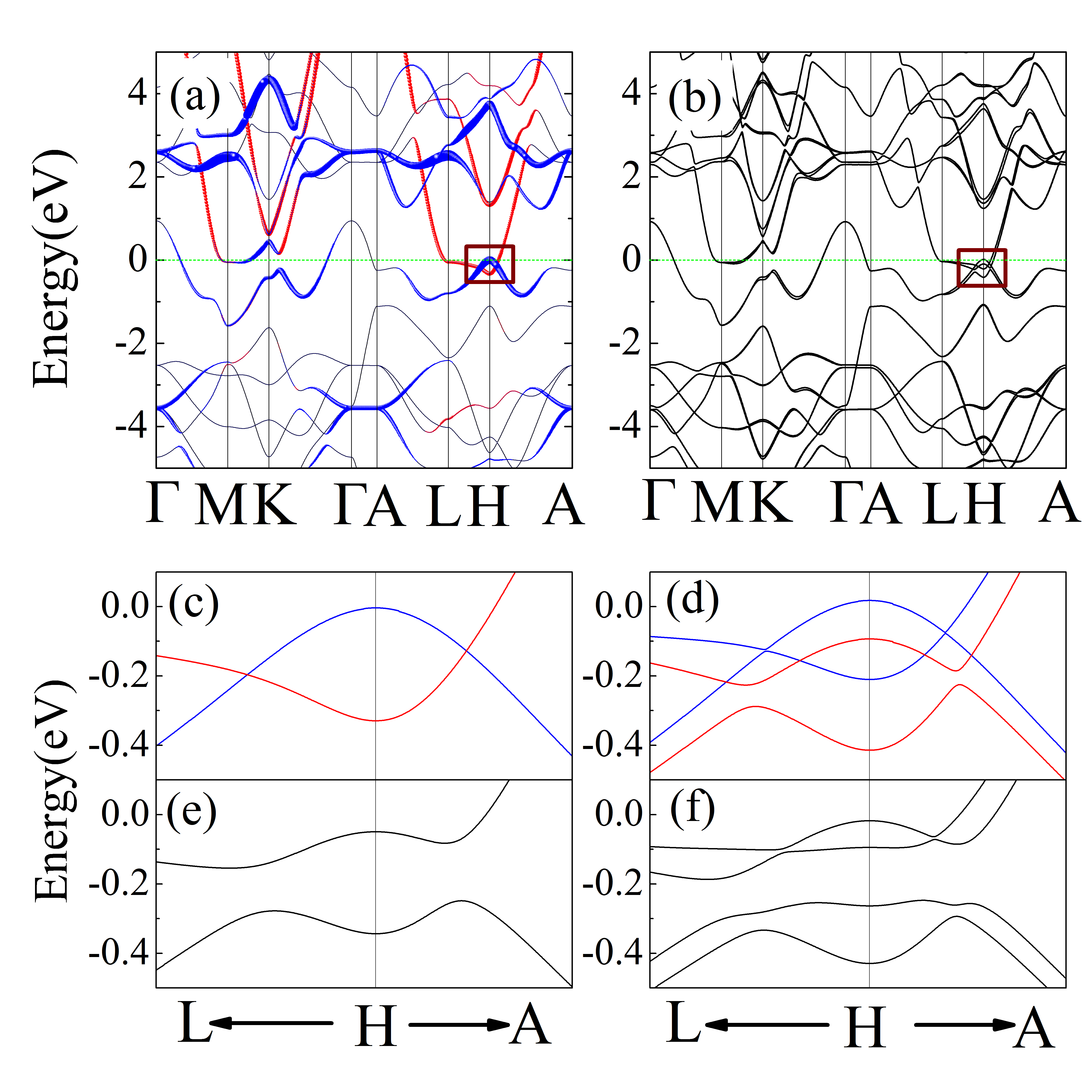
Here we discuss our band structure results for InNbS2. We perform its density functional GGA calculation by using a full potential linear muffin tin orbital (FP–LMTO) method FPLMTO and also cross check the results with linearized augmented plane wave method as implemented in WIEN2K package WIEN2K . Both methods provide identical electronic structures. The orbital character analysis shows that 3 and 3 bands of S atoms are mainly located at -14 to -12 eV and -7 to -1 eV, respectively. This indicates that the S–3 and S–3 orbitals are almost completely filled. Nd–5 states, which are mainly located between -1 and 4 eV, have also a spectral weight between -7 and -1 eV, indicating a considerable hybridization between Nb and S. On the other hand, In–5 bands are distributed mainly above -1 eV. As shown in Fig.2(a), the bands around the Fermi level are mainly contributed by Nb–5/5 and In–6/6 states. The Nb–5/5 bands are higher in energy than the In–6/6 states, however, there is a band inversion around H point as shown in Fig. 2(c). This band inversion has also been confirmed by the modified Becke-Johnson (mBJ) exchange potential calculations mBJ . Since L–H–A plane possess mirror symmetry, the In–6/6 (Nb-5/5) states around H point can be classified in terms of the mirror eigenvalues (), as shown in Fig. 2(c). Combining with the time reversal symmetry, this band inversion guarantees a nodal line in the L–H–A plane TlTaSe2 ; PbTaSe2 . The schematics of the nodal lines in InNbS2 is shown in Fig. 1(c).
To clarify the origin of the band inversion at H point, we calculate the electronic structure of InNbS2 by applying an in–plane tensile strain. We denote the magnitude of the in–plane strain by , where and denote lattice parameters of the strained and unstrained systems, respectively. Our calculation reveals that the energy difference between In–6px/6py state and Nb–5d/5dxy states decreases as the in–plane tensile strain increases, and when the in–plane strain becomes larger than 7%, the band inversion at H point disappears. Therefore, the band inversion originates from the crystal field effect instead of SOC.
To explore the role of the mirror symmetry, we break it by shifting a Nb atom by 0.01 along direction. Without mirror symmetry, the In–6/6 and Nb–5/5 states belong to the same irreducible representation and can hybridize with each other. Thus, the band crossing around the H point becomes gapped as shown in Fig. 2(e). This clearly demonstrates that the nodal line in InNbS2 is indeed protected by the mirror symmetry.
As a relativistic effect, SOC always exists. Thus we also perform the calculation to check the effect of SOC. Without inversion, SOC splits each band into two branches as shown in Fig. 2(b). As a result, there are spinfull bands near the Fermi level as shown in Fig.2(d). Due to the mirror symmetry at L–H–A plane, we can classify these four bands by mirror eigenvalues . Two red bands have mirror eigenvalues , while blue ones have mirror eigenvalues . Since SOC does not eliminate the band inversion, there are two separate Weyl rings around the H point. This unique two separate nodal lines can have unique surface state as discussed in Refs. TlTaSe2 ; PbTaSe2 ; Ca3P2 . When mirror symmetry is broken, four bands around H point are found to belong to the same irreducible representation. Consequently the Weyl rings are gapped out as shown in Fig. 2(f). This again shows that the mirror symmetry play a key role in protecting the nodal lines in InNbS2.
IV IV. Results for InNbSe2
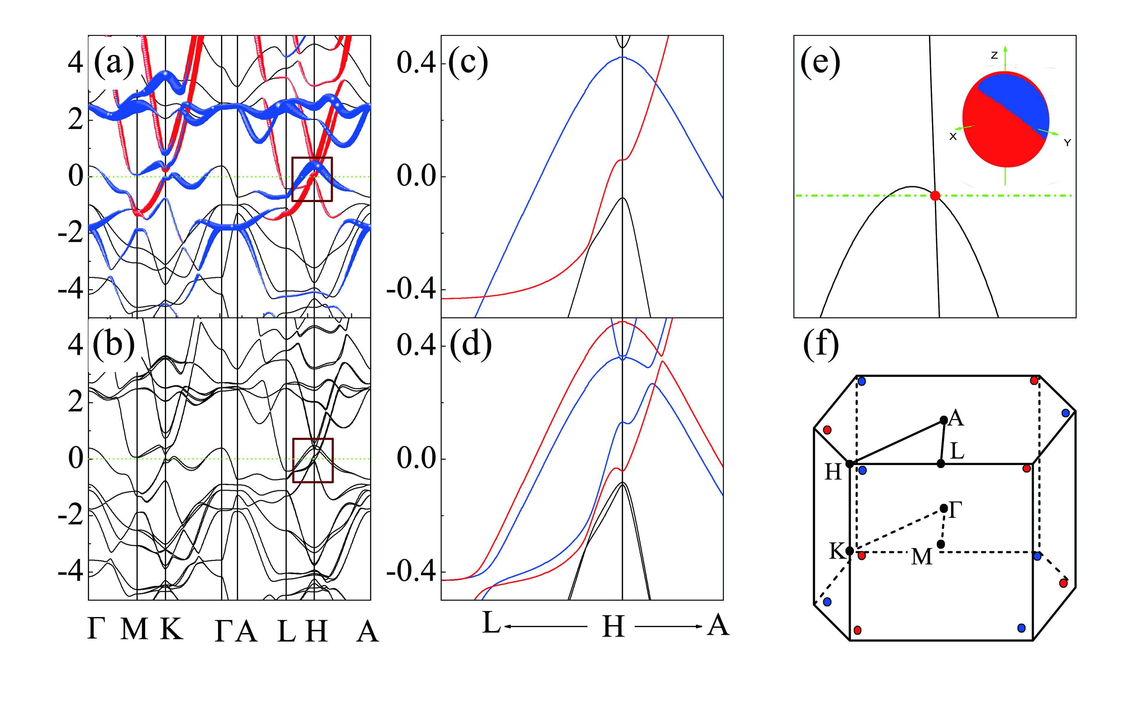
We now discuss our band structure calculation for InNbSe The results without and with SOC are shown in Figs. 3(a) and (b), respectively. Our orbital–character analysis reveals that the states near the Fermi level are mainly contributed by Nb–5d/5dxy (denoted by red color) and In–6px/6py (denoted by blue color). However, both GGA and mBJ calculations predict that the energy of Nb–5d/5dxy is higher than In–6px/6py at the H point. As a result, there is also a band inversion around the H point, like the case of InNbS2. This is shown in Fig. 3(a). Again, based on the mirror symmetry, the bands around the H point can be classified by their mirror eigenvalues. As shown in Fig. 3(c), the band with a mirror eigenvalue -1 (+1) is marked by blue (red). Thus, similar with InNbS2, time reversal symmetry and the band inversion result in a nodal line around the H point at the mirror plane.
When SOC is included in the calculation, two crossing bands around the H point split into four bands as shown in Fig. 3(b). The detailed band structure around the H point marked in Fig. 3(b) is shown in Fig. 3(d). Different from the situation in InNbS2, the mirror eigenvalues of the two bands near the Fermi energy are the same (i.e. ). Thus, these bands are hybridized and open a gap. There are no more nodal lines in this material. Interestingly, our further calculation shows that InNbSe2 becomes a Weyl semimetal with 12 Weyl nodes in the first BZ, as shown in Fig. 3(e) and (f). These 12 Weyl points are related with each other by crystal symmetry, consequently they have the same energy. The Weyl points are searched for by scanning the whole BZ.
To confirm the existence of the Weyl points in InNbSe2, we perform Berry curvature integration based on a computational scheme proposed by Fukui et alChern-1 . We define a small cubic region surrounding each Weyl point. A quantity , which is often called the field strength, is defined asChern-1 ; Chern-2 :
where is a vector at th mesh point, s=1–6 denotes each of six faces of the cube, and are vectors between nearest mesh points for the two directions of the vector on the surface of the cube, is th smallest closed path passing by the points and its nearest mesh point. In this formula, the Chern number is given by the sum over coarse mesh of phases : . The Bloch wave functions are obtained from our first–principles calculations. We employ the 1515 k-mesh on each of the six faces of the cube, which we found to be sufficient for numerical convergence. We calculate the Chern number of the Weyl point located at (0.298, 0.298, 0.444) using this method and obtain the numerical result equal to . The location of this and other Weyl points is schematically shown in Fig. 3(f).
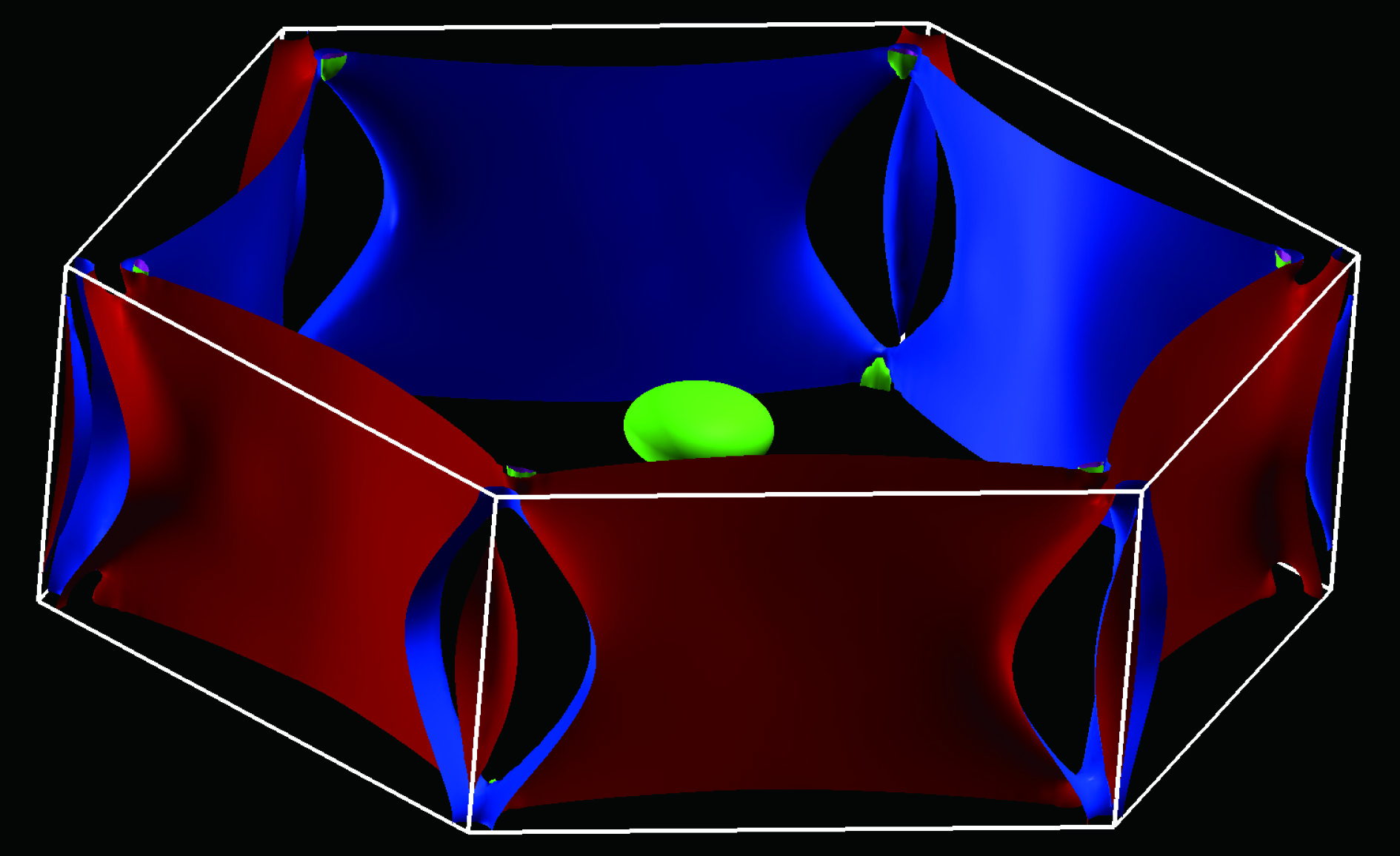
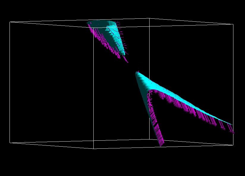
We notice that the Weyl points here exist at the boundaries between electron and hole pockets, therefore the compound can be classified as a type II WSM. Our Fig. 3(e) showing a detailed band dispersion in the vicinity of one Weyl point is very similar to the case of WTe2WTe2 where this new type of Weyl points has been recently introduced. They appear due to the tilting term in the linear Weyl Hamiltonian which has led to a finer classification of topological semimetalsWTe2 . Around the Weyl points, the energy spectrum can been written as: . As a result, we expect that InNbSe2 will display negative magnetoresistence related to chiral anomaly only when the direction of the magnetic field falls within the cone where WTe2 (i.e. the blue area in Fig. 3(e)) . We monitor the contact between electron and hole pockets in InNbSe2 by computing the constant energy surface with a slightly shifted position (by 0.2 eV up) of the Fermi level for stoichiometric compound. The result is shown in Fig. 4(a) where the green–magenta surface is the hole pocket while the red–blue one is the electron pocket. We can see that the hole pocket almost touches the electron pocket near the position of the Weyl point. Fig.4(b) shows the same in the immediate vicinity of the Weyl point together with the spin distribution of electronic states shown by arrows. For an ideal Weyl Hamiltonian, the spins are either parallel or antiparallel to the velocities corresponding to the positive/negative chiralities. In real compounds such as InNbSe2, considered here, this becomes only approximate, and as seen in Fig. 4(b), spins show a rather high degree of anisotropy.
V V. Fermi Arcs and Effect of Surface Disorder
In order to examine the Fermi arc surface states of InNbSe2 we determine the one–electron energy bands of 6 unit–cell (24 atomic layers) slab structure using the full potential linear muffin–tin orbital (FP–LMTO) methodFPLMTO . The slab is extended along (001) direction and terminated by Se atomic layer at the top and by In atomic layer at the bottom. The spacing between the slabs is set to 12Å. The distance between In and Se atoms is largest in the original unit cell which together with the quasi–two–dimensionality of the crystal structure prompts that this should be most easily cleavable surface in an experimental setup.
In order to compute the surface Fermi states, we compute surface projected imaginary Green functions
where we set , and where the surface projector operator is chosen as a sum over 4 top/bottom atomic layers
Here are the solutions of the radial Schroedinger equation inside a muffin–tin sphere of atom taken with the spherically symmetric part of the potentialphidot .
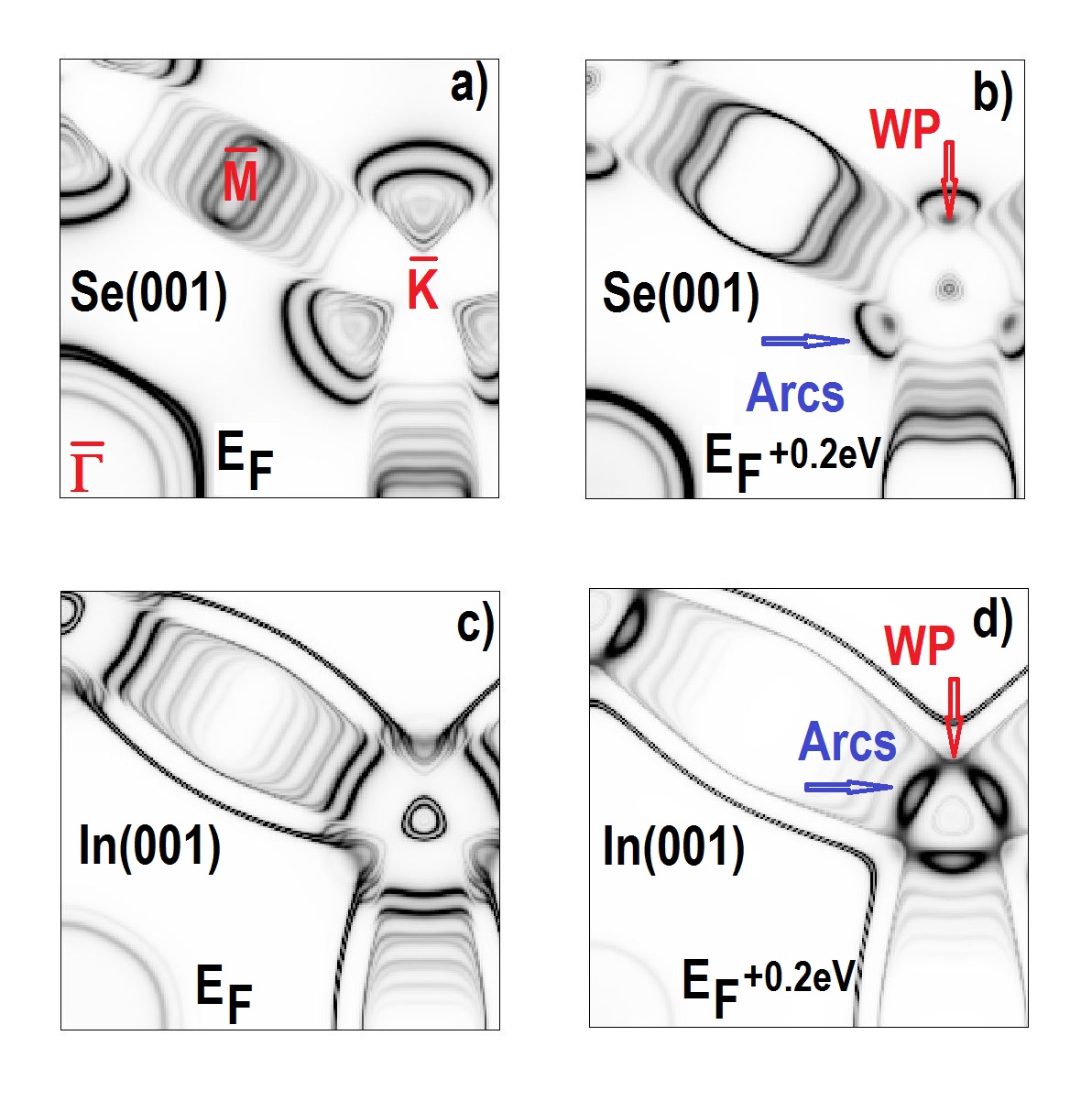
Fig. 5 shows the result of our calculation, where we visualize as a function of by a color (white is 0 and black is /) within a part of the planar Brillouin Zone corresponding to the (001) surface unit cell. We distinguish cases for Se terminated (plots a,b) and In terminated (plots c,d) surfaces. Since the Weyl points are located not exactly at the Fermi level, we plot for the energy (plots a, c) as well as for the energy (plots b, d) which corresponds to the location of the Weyl points. We note that although (001) surface should be easy to cleave, the chosen atomic configuration assumes that the Weyl points of opposite chiralities project onto the same –point in the surface BZ. It means that the Fermi arcs extending between opposite chiral charges can potentially start and end at the same projected Weyl point. We found this to be the case for the Se terminated surface where small arcs are clearly visible especially on Fig.5(b) corresponding to the position of the Fermi level tuned to the Weyl point. The situation is more complicated for the In terminated surface where there are essentially two lines that are resolved as connecting the Weyl points on Fig.5(d). We interpret one line to be potentially the Fermi arc and another one to be either a regular surface state or a bulk Fermi state projected to the surface BZ.
In a recent work Disorder we argued, based on a simulation of a tight–binding model, that the Fermi arcs should be more surface disorder tolerant than the regular surface states especially in the vicinity of the Weyl points where the arcs electronic wave functions are extended well into the bulk and become less sensitive to the surface disorder. We also found that the particular sensitivity to the surface disorder depends on the shape of the Fermi arc with the straight arc geometry showing its most disorder tolerance. Surface disorder is inevitable in a real experimental setting with vacancies being its primary source. It is therefore interesting to examine this effect in our proposed InNbSe2 WSM.
In order to perform simulation of vacancies on the surface of InNbSe2, we use a combination of DFT with a coherent potential approximation (CPA)CPA , a self–consistent method that allows to extract disorder induced self–energies from the FP–LMTO calculation. Our recent implementation within FP LMTO method is described in Ref. Disorder . Figure 6(a,b) shows evolution of the one–electron Fermi states of the InNbSe2 slab structure that are projected onto the Se terminated surface for two concentrations, =0.05 and =0.1, respectively, of substitutional vacancies that we impose at its topmost Se layer. For both concentrations, the Fermi arcs are still visible and increasing the disorder results in broadening the arcs especially in the regions always from the Weyl points. Since the arcs electrons are continuously connected to the bulk Weyl points, the area in the vicinity of the Weyl points is less affected by disorder. We can contrast this behavior with the regular surface states which we expect to be more susceptible to surface disorder. We do not impose any bulk disorder in this calculation, therefore the bulk states projected onto the surface BZ are unaffected by the surface vacancies.
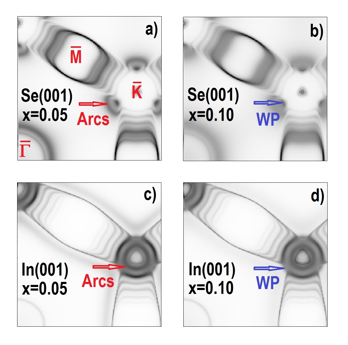
The situation is more complicated for the Fermi arcs appeared at the In terminated (001) surface. Figure 6(c,d) shows their behavior for =0.05 and =0.1, respectively. We notice that the arcs that connect the Weyl points in Fig 5(d) slightly change their shape with disorder which possibly connected to the effect induced by the real part of the disorder self–energy One state is seen in this simulation to get closer to the point of the surface BZ while another state has its shape resembling a regular bulk Fermi state projected onto the surface BZ. Both states acquire much less broadening if we compare them with other surface states that broaden a lot and almost disappear when x=0.1. As these arcs show a lot less curvature than the arcs resolved at Se terminated surface, we therefore speculate that this is likely the effect of the disorder tolerance for the straight Fermi arcs that we proposed in our recent work Disorder .
VI VI. Summary
In summary, by using first–principles calculations, we investigated topological properties of InNbS2 and InNbSe2. Our theoretical analysis showed that InNbS2 is a nodal line semimetal even with the included spin orbit coupling as long as the mirror symmetry preserved. This significant feature is different from previously proposed materials which normally neglects SOC. InNbSe2 is proposed to be a Type II WSM with 12 Weyl nodes at the same energy level. We also studied the Fermi arcs surface states and their tolerance to the surface disorder effects. These two compounds are quasi–2D and easy to cleave, therefore can potentially serve as an interesting platform for further experimental studies of their topological electronic states.
VII Acknowledgement
The work was supported by National Key R&D Program of China (No. 2017YFA0303203), the NSFC (No. 11525417, 11374147, 51572085), National Key Project for Basic Research of China (Grant No. 2014CB921104), the Natural Science Foundation of Jiangsu Province (Grants No. BK20170821), the Priority Academic Program Development of Jiangsu Higher Education Institutions. S.S. was supported by NSF DMR (Grant No. 1411336).
References
- (1) X. Wan, A. M. Turner, A. Vishwanath, and S. Y. Savrasov, Phys. Rev. B 83, 205101 (2011).
- (2) L. Balents, Physics 4, 36 (2011).
- (3) S. M. Young, S. Zaheer, J. C. Y. Teo, C. L. Kane, E. J. Mele, and A. M. Rappe, Phys. Rev. Lett. 108, 140405 (2012).
- (4) B.-J. Yang and N. Nagaosa, Nature Commun. 5, 4898 (2014)
- (5) Z. Gao, M. Hua, H. Zhang, and X. Zhang, Phys. Rev. B 93, 205109 (2016)
- (6) Z. Wang, Y. Sun, X.-Q. Chen, C. Franchini, G. Xu, H. M. Weng, X. Dai, and Z. Fang, Phys. Rev. B 85, 195320 (2012).
- (7) Z. Wang, H. M. Weng, Q. Wu, X. Dai, and Z. Fang, Phys. Rev. B 88, 125427 (2013).
- (8) Q. D. Gibson, L. M. Schoop, L. Muechler, L. S. Xie, M. Hirschberger, N. P. Ong, R. Car, and R. J. Cava, Phys. Rev. B 91, 205128 (2015).
- (9) Y. Du, B. Wan, D. Wang, L. Sheng, C. Duan and X. Wan, Sci. Rep. 5, 14423 (2015).
- (10) A. A. Burkov, M.D. Hook, and L. Balents, Phys. Rev. B 84, 235126 (2011)
- (11) H. Weng, Y. Liang, Q. Xu, R. Yu, Z. Fang, X. Dai, and Y. Kawazoe, Phys. Rev. B 92, 045108 (2015)
- (12) R. Yu, H. Weng, Z. Fang, X. Dai and X. Hu, Phys. Rev. Lett. 115, 036807 (2015)
- (13) Y. Kim, B. J. Wieder, C. L. Kane, and A. M. Rappe, Phys. Rev. Lett. 115, 036806 (2015)
- (14) X. Wan, A. Vishwanath, and S. Y. Savrasov, Phys. Rev. Lett. 108, 146601 (2012).
- (15) V. Aji, Phys. Rev. B 85, 241101 (2012).
- (16) D. T. Son and B. Z. Spivak, Phys. Rev. B 88, 104412 (2013).
- (17) K.-Y. Yang, Y.-M. Lu, and Y. Ran, Phys. Rev. B 84, 075129 (2011).
- (18) S. A. Parameswaran, T. Grover, D. A. Abanin, D. A. Pesin, and A. Vishwanath, Phys. Rev. X 4, 031035 (2014).
- (19) A. C. Potter, I. Kimchi and A. Vishwanath, Nature Communications 5, 6161 (2014).
- (20) A. A. Soluyanov, D. Gresch, Z. Wang, Q. Wu, M. Troyer, X. Dai and B. A. Bernevig, Nature 527, 495 (2015).
- (21) T. E. O’Brien, M. Diez, and C. W. J. Beenakker, Phys. Rev. Lett. 116, 236401 (2016).
- (22) G. Xu, H. M. Weng, Z. Wang, X. Dai, and Z. Fang, Phys. Rev. Lett. 107, 186806 (2011).
- (23) H. Weng, C. Fang, Z. Fang, B. A. Bernevig, and X. Dai, Phys. Rev. X 5, 011029 (2015).
- (24) S. M. Huang, et al., Nat. commun. 6, 7373 (2015).
- (25) C. Shekhar, et al. Nat. Phy. 11, 645 (2015).
- (26) N. Xu, et al. Nat. Commun. 7, 11006 (2016).
- (27) S.-Y. Xu, et al. Nat. Phys. 11, 748 (2015).
- (28) L. Huang, et al. Nat. Materials 15, 1155-1160 (2016).
- (29) G. Autès, D. Gresch, M. Troyer, A.A. Soluyanov, and O.V. Yazyev, Robust. Phys. Rev. Lett. 117, 066402 (2016).
- (30) Su-Yang Xu, et al. arXiv:1603.07318 (2016).
- (31) B. Q. Lv, et al., Phys. Rev. X 5, 031013 (2015).
- (32) B. Q. Lv, et al., Nat. Phys. 11, 724–727 (2015).
- (33) S.-Y. Xu, et al., Science 349, 613 (2015).
- (34) D. F. Xu et al., Chin. Phys. Lett. 32, 107101 (2015).
- (35) C. Fang, Y. Chen, H.-Y. Kee and L. Fu, Phys. Rev. B 92, 081201(2015).
- (36) Q. Xu, R. Yu, Z. Fang, X. Dai, and H. Weng, arXiv: 1608.03172 (2016).
- (37) H. Huang, J. Liu, D. Vanderbilt, and W. Duan, Phys. Rev. B 93, 201114 (2016).
- (38) Y. Du, F. Tang, D. Wang, L. Sheng, E.-j. Kan, C.-G. Duan, S. Y. Savrasov, and X. Wan, npj Quantum Materials 2, 3 (2017).
- (39) K. Mullen, B. Uchoa, and D. T. Glatzhofer, Phys. Rev. Lett. 115, 026403 (2015).
- (40) L. S. Xie, L. M. Schoop, E. M. Seibel, Q. D. Gibson, W. Xie, and R. J. Cava, APL Materials 3, 083602 (2015).
- (41) M. Zeng, C. Fang, G. Chang, Y. A. Chen, T. Hsieh, A. Bansil, H. Lin, L. Fu, arXiv:1504.03492 (2015)
- (42) Y.-H. Chan, C.-K. Chiu, M. Y. Chou, and A. P. Schnyder, Phys. Rev. B 93, 205132 (2016)
- (43) G. Bian, et al., Phy. Rev. B 93, 121113(R) (2016)
- (44) G. Bian et al., Nature Communs. 7, 10556 (2015)
- (45) T. T. Heikkila and G. E. Volovik, arXiv: 1504.05824 (2015)
- (46) N. B. Kopnin, T. T. Heikkila, and G. E. Volovik, Phys. Rev. B 83, 220503 (2011).
- (47) J. P. Perdew, K. Burke, and M. Ernzerhof, Phys. Rev. Lett. 77, 3865 (1996).
- (48) N. Karnezos, L. B. Welsh and M. W. Shafer, Phy. Rev. B 11, 1808-1917 (1975).
- (49) C. S. Sunandana, K. Chandrasekaran, G. Aravamudan and G. V. Subbarao, J. Less-Common Metals, 84, 115 (1982).
- (50) E. A. Marseglia, International Reviews in Physical Chemistry 3, 177 (1983).
- (51) S. Y. Savrasov, Linear-response theory and lattice dynamics: a muffin-tin-orbital approach, Phys. Rev. B 54, 16470 (1996).
- (52) P. Blaha, K. Schwarz, G. K. H. Madsen, D. Kvasnicka, and J. Luitz, WIEN2K, An Augmented Plane Wave+ Local Orbitals Program for Calculating Crystal Properties (Karlheinz Schwarz, Technische Universitat Wien, Austria, 2001).
- (53) F. Tran and P. Blaha, Phys. Rev. Lett. 102, 226401 (2009).
- (54) Takahiro Fukui, Yasuhiro Hatsugai and Hiroshi Suzuki, J. Phys. Soc. Jpn., 74, 6 (2005).
- (55) M. Taillefumier, V. K. Dugaev, B. Canals, C. Lacroix, and P. Bruno, Phys. Rev. B 78, 155330 (2008).
- (56) In fact, both the LMTO and LAPW methods assume improved projectors that include both the radial wave functions and their energy derivatives in order to better describe orbital partial characters of the one–electron states. See, O. K. Andersen, Phys. Rev. B 12, 3050 (1975).
- (57) G. Resta, S.-T. Pi, X. Wan, S. Y. Savrasov, arXiv:1708.02415 (2017).
- (58) For a review, see, e.g., Yonezawa, F. & Morigaki, K. Coherent potential approximation: basic concepts and applications. Prog. Theo. Phys. Supp. 53, 1–76 (1973).