Observation of Dirac surface states in the hexagonal PtBi2, a possible origin of the linear magnetoresistance
Abstract
The nonmagnetic compounds showing extremely large magnetoresistance are attracting a great deal of research interests due to their potential applications in the field of spintronics. PtBi2 is one of such interesting compounds showing large linear magnetoresistance (MR) in its both the hexagonal and pyrite crystal structure. We use angle-resolved photoelectron spectroscopy (ARPES) and density functional theory (DFT) calculations to understand the mechanism of liner MR observed in the hexagonal PtBi2. Our results uncover for the first time linear dispersive surface Dirac states at the -point, crossing Fermi level with node at a binding energy of 900 meV, in addition to the previously reported Dirac states at the -point in the same compound. We further notice from our dichroic measurements that these surface states show an asymmetric spectral intensity when measured with left and right circularly polarized light, hinting at a substantial spin polarization of the bands. Following these observations, we suggest that the linear dispersive Dirac states at the and -points are likely to play a crucial role for the linear field dependent magnetoresistance recorded in this compound.
The property of magnetoresistance in the nonmagnetic solids has majorly two types of behaviour under the external magnetic fields. While the linear field dependent magnetoresistance as observed in graphene Singh et al. (2012), topological insulators Bi2Te3 and Bi2Se3 Qu et al. (2010); Wang et al. (2012), Ag2+δTe/Se Xu et al. (1997); Lee et al. (2002), Dirac semimetals Cd3As2 Liang et al. (2014); Feng et al. (2015) and Na3Bi Kushwaha et al. (2015), and type-I Weyl semimetals NbAs(P) Ghimire et al. (2015); Shekhar et al. (2015); Wang et al. (2016) and TaAs Huang et al. (2015); Zhang et al. (2015) is explained based on the linear dispersive Dirac states present near the Fermi level Abrikosov (1998, 2003), the quadratic field dependent MR as observed in the type-II Weyl semimetals WTe2 and MoTe2 Ali et al. (2014); Zhou et al. (2016), LaSb Zeng et al. (2016), ZrSiS Lv et al. (2016), and Bi Yang (1999) is explained based on the charge compensation Ali et al. (2014). However, the role of charge compensation for the XMR of these compounds is still not clear as some reports recently demonstrated quadratic field dependent MR without charge balance Zandt et al. (2007); Thirupathaiah et al. (2017). Moreover, the theory based on the impurity scattering or crystal disorder is inevitably brought into the above two cases and as well to the subquadratic field dependent MR Fatemi et al. (2017); Parish and Littlewood (2003); Ping et al. (2014). The other existing mechanisms include metal-insulator transition Khveshchenko (2001); Kopelevich et al. (2006); Wang et al. (2014); Zhao et al. (2015); Xiang et al. (2015) and strong spin-orbit interactions Jiang et al. (2015); Das et al. (2016). Thus, there is no clear consensus yet on the mechanism of magnetoresistance in the nonmagnetic solids.
PtBi2 is a very interesting compound as it shows MR in both the hexagonal Yang et al. (2016) and pyrite structures Gao et al. (2016). Astonishingly, the pyrite PtBi2 has been found to show the highest MR observed among the known nonmagnetic metals so far Xu et al. (1997); Lee et al. (2002); Liang et al. (2014); Ali et al. (2014); Feng et al. (2015); Shekhar et al. (2015); Zhou et al. (2016), which also has been predicted as a 3-dimensional Dirac semimetal Gibson et al. (2015). Therefore, understating the mechanism of extremely large MR in this compound is essential due to its potential applications. While in the pyrite structure the extremely large MR is attributed to its semimetalic nature Gao et al. (2016), the large linear MR observed in the hexagonal phase is explained based on the crystal disorder theory Yang et al. (2016); Yao et al. (2016). Here, we report on the electronic structure of hexagonal PtBi2 using the ARPES technique and first-principles calculations. Our studies suggest that PtBi2 has two different surface terminations as the experimental band structure looks different from different cleavages. Our ARPES measurements demonstrate linear dispersive surface Dirac states near the Fermi level with a node at 150 meV below the Fermi level () at the -point with a 6-fold rotational symmetry in the plane. Thus, there exists 6 Dirac cones of this type in a Brillouin zone. This observation is consistent with a previous ARPES report Yao et al. (2016) on this compound. Interestingly, in addition to this, we have uncovered for the first time an another surface Dirac cone at the zone center with a node at 900 meV below . Much like in BiPd Thirupathaiah et al. (2016), the Dirac states at the zone center in PtBi2 show a gap opening as a function of photon energy, possibly due to a surface-bulk hybridization. Based on these studies, we suggest that the linear MR observed in the hexagonal PtBi2 could have originated from the linear dispersive surface states in the quantum limit, like in the case of topological insulators Qu et al. (2010); Wang et al. (2012) where the large linear MR is observed only from the surface band structure.
High quality single crystals of hexagonal PtBi2 were grown using floating zone technique Cry . The crystals have a platelet-like shape with shiny surface. The crystals were structurally characterized using powder X-ray diffraction to confirm the bulk purity and the hexagonal crystal structure with space group. ARPES measurements were carried out in BESSY II (Helmholtz Zentrum Berlin) synchrotron radiation facility at the UE112-PGM2b beam-line using the ”13-ARPES” Borisenko (2012); Borisenko et al. (2012) end station equipped with SIENTA R4000 spectrometer. The total energy resolution was set between 5 and 15 meV, depending on the incident photon energy. The measurements were performed at T = 1 K. Another set of ARPES measurements were performed in the Diamond light source at I05 beamline equipped with SIENTA R4000 spectrometer. The sample temperature at Diamond was always below 10 K and the energy resolution was set between 10 and 20 meV depending on the incident photon energy.
Self-consistent band structure calculations were performed on the hexagonal crystal structure of PtBi2 having the lattice constants = = 6.572 Å and = 6.166 Å using the linear muffin-tin orbital (LMTO) method Andersen (1975) in the atomic sphere approximation (ASA) as implemented in PY LMTO computer code Antonov (2004). The Perdew-Wang parameterization Perdew and Wang (1992) was used to construct the exchange correlation potential in the local density approximation (LDA). Spin-orbit coupling was taken into account at the variational step.
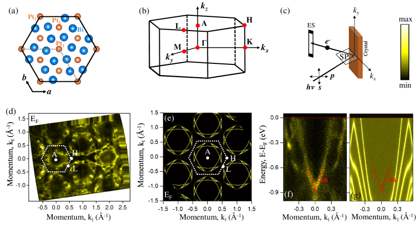
The electronic structure of PtBi2 is shown in Fig. 1 obtained by means of ARPES and DFT calculations. The ARPES data are measured using -polarized light with a photon energy of 100 eV. The data are taken at a sample temperature of 1 K. We estimate that 100 eV photons detect the bands nearly from the =5.5 plane using an inner potential of Pt of 25 eV Ichikawa et al. (2003), i.e., from the plane. Fig. 1(a) shows the hexagonal crystal structure of PtBi2 projected onto the -plane. Fig. 1(b) shows 3D view of the Brillouin zone in which various high symmetry points are located. In Fig. 1(c) we schematically show the measuring geometry where the - and -plane polarized lights are defined with respect to the analyzer entrance slit (ES) and the scattering plane (SP). Fig. 1(d) shows the experimental Fermi surface (FS) map in the plane extracted by integrating over an energy window of 20 meV centered at . Fig. 1(f) shows the FS map derived from DFT calculations. Fermi surface obtained in our studies [see Fig. 1 (d) and (e)] is inline with the hexagonal crystal structure of PtBi2[see Fig. 1(a)]. Fermi surface obtained in our studies is inline with the hexagonal crystal structure of PtBi2 [see Fig. 1(a)]. Energy distribution map (EDMs) along the - high symmetry lines is shown in Fig. 1 (h). In Fig. 1 (h), the red-dashed lines represent linearly dispersive Dirac surface states with a node at 900 meV. Calculated band dispersions along the - high symmetry lines are shown in Fig. 1 (i). Note here that the Fermi level of the calculated band structure is shifted about 200 meV towards the lower-binding energy to match with the experiment. A similar observation was also made in the previous ARPES report of this compound Yao et al. (2016).
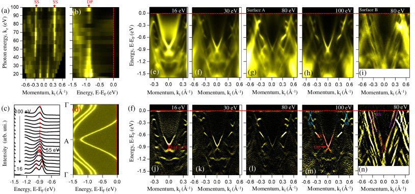
Next, we show photon energy dependent ARPES measurements performed to understand the dependent band structure of this compound. Fig. 2(a) shows the Fermi surface map measured using -polarized light in the plane. Fig. 2(b) shows the EDM taken along the - high symmetry line at =0. Energy distribution curves (EDCs) as a function of incident photon energy are shown in Fig. 2(c). Band dispersions in the - symmetry line derived from the DFT calculations are shown in Fig. 2(d). Figs. 2(e)-(h) depict EDMs measured using various photon energies. Figs. 2(j)-(m) depict second derivatives of Figs. 2(e)-(h). In Fig. 2(i), we show EDM taken from a different cleavage (say Surface B) surface using -polarized light with a photon energy of 80 eV, while the rest of the data are measured from another cleavage (say Surface A). Fig. 2(n) depicts the second derivative of Fig. 2(i). In the figures, the red- and blue-dashed lines represent the surface states (SS), while the pink-dashed lines represent the bulk states (BS).
In the map shown in Fig. 2(a), we can clearly notice that the two Fermi sheets shown by the red down-arrows have negligible warping. In principle, surface states show independent band structure. On the other hand, our bulk band structure calculations suggest a strong warping of the Fermi sheets in the plane (not shown) . Therefore, from these observations we suggest that these Fermi sheets are from the surface contribution. This is further confirmed from the EDM taken along the - direction [see Fig. 2(b)] where one can notice a flat dispersion for the Dirac point (DP) at 900 meV of the binding energy and no such band is found from a similar EDM derived from the calculations [see Fig. 2(d)]. Interestingly, from the energy distribution curves (EDCs) extracted as a function of photon energy we noticed that the Dirac states at the zone center are gapped when measured with the photon energy 55 eV. This is further demonstrated from the photon energy dependent EDMs shown in Figs. 2(e)-(h) and from the corresponding second derivatives shown in Figs. 2(j)-(m). The estimated maximum energy gap is of 145 meV when measured with 16 eV of photon energy [see Fig. 2(j)]. A similar observation was made earlier in the case of noncentrosymmetric BiPd Thirupathaiah et al. (2016). There, it was suggested that the gap opening is due to the hybridization between the surface and the bulk states located in the same binding energy range. In the present case as well it could be the similar scenario as the bulk bands disperse in the direction over a window of 1 eV of binding energy. As can be seen in Fig. 2(d), the binding energy of the band at is of 0.65 eV whereas at the binding energy of the same band is of 1.5 eV. Therefore, as the surface states show a finite penetration depth into the solid Autès et al. (2015); Li et al. , it is highly likely to have a surface-bulk hybridization which may lead to the gap opening at the Dirac point. On Fig. 2(m), we have shown schematically another set of Dirac surface states by the blue-dashed lines located at the -point having a Dirac point at 150 meV with a 6-fold rotational symmetry. Thus, there are in total 6 Dirac cones of this type in a BZ. This observation is in good agreement with previous ARPES report on this compound Yao et al. (2016). The electronic structure of PtBi2 seems to be cleavage dependent. As can be seen in Figs. 2(i) and (n), the EDM taken from the cleavage surface B shows no signatures of the Dirac-like surface states when compared to the data taken on the cleavage surface A. Moreover, the band structure highlighted by pink-dashed lines shown in Figs. 2(i) and (n) look much alike the bulk band structure derived from the DFT calculations [see Fig. 1(i)].
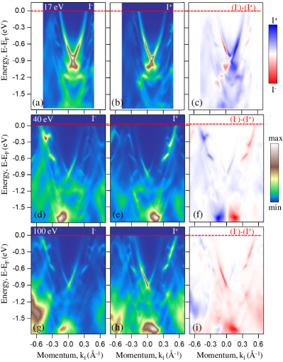
Next we show the circular dichroic ARPES measurements. Energy distribution map (I-) shown in Fig. 3(a) is measured using a left-circular polarized light with a photon energy of 17 eV. Similarly, EDM (I+) shown in Fig. 3(b) is measured using a right-circular polarized light. Fig. 3(c) is the resultant spectra after the subtraction (I--I+). Figs. 3(d)-(i) are analogous data to Figs. 3(a)-(c) but measured with photon energies of 40 and 100 eV. Generally, in spin-orbit coupled systems the helicity of light can couple to the electron spin degree of freedom through the total angular momentum. Therefore, the helicity dependent spectral intensity can provide indirectly information on the spin polarization of the detected sates Wang et al. (2011); Park et al. (2011); Wang and Gedik (2013). However, it is also argued that such measurements suffer greatly from the final state effects and thus, reversing the dichroic signal among the photon energies Scholz et al. (2013). Nevertheless, as can be seen from the intensity difference spectra [Figs. 3(c), (f) and (i)] taken from a wide range of photon energies (17, 40 and 100 eV), the dichroic signal is consistent at the zone center switching the spectral intensity of the Dirac cone as . Interestingly, dichroic signal is noticed also for the Dirac states at the -point, but with opposite sign.
Previous transport Yang et al. (2016) and ARPES studies Yao et al. (2016) on this compound suggested crystal disorder for the observed linear magnetoresistance. On the other hand, our present studies clearly show two sets of linear dispersive Dirac states crossing the Fermi level with nodes located at around 150 meV and 900 meV below . Therefore, based on these observations we suggest that the linear MR observed in this compound could be originated from the linear dispersive surface states. This is argument is inline with the theory based on the Landau levels of the linear dispersive states in the presence of external magnetic field Abrikosov (1998, 2003), where it was suggested that the linear dispersive states without a gap near the Fermi level play a crucial role. In addition, following our circular dichroic measurements we further suggest that the surface states are substantially spin polarized. Therefore, spin polarization of the bands also may play a vital role for the magnetoresistance Jiang et al. (2015) of this compound.
In conclusion, we studied the low-energy band structure of the hexagonal PtBi2 by means of ARPES technique and DFT calculations. Our studies uncover for the first time linearly dispersive Dirac states near -point, crossing the Fermi level with a node at 900 meV below . In addition, another surface Dirac cone is found at the -point-point with a node at 150 meV below . We further notice from the circular dichroic measurements that these surface states show a significant dichroic signal switching as . Following these studies, we suggest that the linear dispersive spin polarized Dirac states found at both the -point and -point points could be a possible origin for the large linear MR observed in this compound rather than the crystal disorder that was suggested earlier for the same.
This work was supported under the DFG grant BO 1912/7-1. S.T. acknowledges support by the Department of Science and Technology, India through the INSPIRE-Faculty program (Grant number: IFA14 PH-86). We acknowledge Diamond Light Source for time on Beamline/Lab I05 under Proposal SI15936-1.
References
- Singh et al. (2012) R. S. Singh, X. Wang, W. Chen, Ariando, and A. T. S. Wee, Applied Physics Letters 101, 183105 (2012).
- Qu et al. (2010) D.-X. Qu, Y. S. Hor, J. Xiong, R. J. Cava, and N. P. Ong, Science 329, 821 (2010).
- Wang et al. (2012) X. Wang, Y. Du, S. Dou, and C. Zhang, Phys. Rev. Lett. 108, 266806 (2012).
- Xu et al. (1997) R. Xu, A. Husmann, T. Rosenbaum, M. Saboungi, J. Enderby, and P. Littlewood, Nature 390, 57 (1997).
- Lee et al. (2002) M. Lee, T. F. Rosenbaum, M.-L. Saboungi, and H. S. Schnyders, Phys. Rev. Lett. 88, 066602 (2002).
- Liang et al. (2014) T. Liang, Q. Gibson, M. N. Ali, M. Liu, R. J. Cava, and N. P. Ong, Nature Materials 14, 280 (2014).
- Feng et al. (2015) J. Feng, Y. Pang, D. Wu, Z. Wang, H. Weng, J. Li, X. Dai, Z. Fang, Y. Shi, and L. Lu, Phys. Rev. B 92, 081306 (2015).
- Kushwaha et al. (2015) S. K. Kushwaha, J. W. Krizan, B. E. Feldman, A. Gyenis, M. T. Randeria, J. Xiong, S.-Y. Xu, N. Alidoust, I. Belopolski, T. Liang, M. Z. Hasan, N. P. Ong, A. Yazdani, and R. J. Cava, APL Materials 3, 041504 (2015).
- Ghimire et al. (2015) N. J. Ghimire, Y. Luo, M. Neupane, D. J. Williams, E. D. Bauer, and F. Ronning, Journal of Physics: Condensed Matter 27, 152201 (2015).
- Shekhar et al. (2015) C. Shekhar, A. K. Nayak, Y. Sun, M. Schmidt, M. Nicklas, I. Leermakers, U. Zeitler, Y. Skourski, J. Wosnitza, Z. Liu, Y. Chen, W. Schnelle, H. Borrmann, Y. Grin, C. Felser, and B. Yan, Nature Physics 11, 645 (2015).
- Wang et al. (2016) Z. Wang, Y. Zheng, Z. Shen, Y. Lu, H. Fang, F. Sheng, Y. Zhou, X. Yang, Y. Li, C. Feng, and Z.-A. Xu, Phys. Rev. B 93, 121112 (2016).
- Huang et al. (2015) X. Huang, L. Zhao, Y. Long, P. Wang, D. Chen, Z. Yang, H. Liang, M. Xue, H. Weng, Z. Fang, X. Dai, and G. Chen, Phys. Rev. X 5, 031023 (2015).
- Zhang et al. (2015) C. Zhang, Z. Yuan, S. Xu, Z. Lin, B. Tong, M. Zahid Hasan, J. Wang, C. Zhang, and S. Jia, ArXiv e-prints (2015), arXiv:1502.00251 [cond-mat.mtrl-sci] .
- Abrikosov (1998) A. A. Abrikosov, Phys. Rev. B 58, 2788 (1998).
- Abrikosov (2003) A. A. Abrikosov, J. Phys. A: Math. Gen. 36, 9119 (2003).
- Ali et al. (2014) M. N. Ali, J. Xiong, S. Flynn, J. Tao, Q. D. Gibson, L. M. Schoop, T. Liang, N. Haldolaarachchige, M. Hirschberger, N. P. Ong, and R. J. Cava, Nature 514, 205 (2014).
- Zhou et al. (2016) Q. Zhou, D. Rhodes, Q. R. Zhang, S. Tang, R. Schönemann, and L. Balicas, Phys. Rev. B 94, 121101 (2016).
- Zeng et al. (2016) L.-K. Zeng, R. Lou, D.-S. Wu, Q. N. Xu, P.-J. Guo, L.-Y. Kong, Y.-G. Zhong, J.-Z. Ma, B.-B. Fu, P. Richard, P. Wang, G. T. Liu, L. Lu, Y.-B. Huang, C. Fang, S.-S. Sun, Q. Wang, L. Wang, Y.-G. Shi, H. M. Weng, H.-C. Lei, K. Liu, S.-C. Wang, T. Qian, J.-L. Luo, and H. Ding, Phys. Rev. Lett. 117, 127204 (2016).
- Lv et al. (2016) Y.-Y. Lv, B.-B. Zhang, X. Li, S.-H. Yao, Y. B. Chen, J. Zhou, S.-T. Zhang, M.-H. Lu, and Y.-F. Chen, Applied Physics Letters 108, 244101 (2016).
- Yang (1999) F. Y. Yang, Science 284, 1335 (1999).
- Zandt et al. (2007) T. Zandt, H. Dwelk, C. Janowitz, and R. Manzke, J. Alloys Compd. 442, 216 (2007).
- Thirupathaiah et al. (2017) S. Thirupathaiah, R. Jha, B. Pal, J. S. Matias, P. K. Das, P. K. Sivakumar, I. Vobornik, N. C. Plumb, M. Shi, R. A. Ribeiro, and D. D. Sarma, Phys. Rev. B (R) 95, 241105 (2017).
- Fatemi et al. (2017) V. Fatemi, Q. D. Gibson, K. Watanabe, T. Taniguchi, R. J. Cava, and P. Jarillo-Herrero, Phys. Rev. B 95, 041410 (2017).
- Parish and Littlewood (2003) M. M. Parish and P. B. Littlewood, Nature 426, 162 (2003).
- Ping et al. (2014) J. Ping, I. Yudhistira, N. Ramakrishnan, S. Cho, S. Adam, and M. S. Fuhrer, Phys. Rev. Lett. 113, 047206 (2014).
- Khveshchenko (2001) D. V. Khveshchenko, Phys. Rev. Lett. 87, 206401 (2001).
- Kopelevich et al. (2006) Y. Kopelevich, J. C. M. Pantoja, R. R. da Silva, and S. Moehlecke, Phys. Rev. B 73, 165128 (2006).
- Wang et al. (2014) K. Wang, D. Graf, L. Li, L. Wang, and C. Petrovic, Sci. Rep. 4 (2014), 10.1038/srep07328.
- Zhao et al. (2015) Y. Zhao, H. Liu, J. Yan, W. An, J. Liu, X. Zhang, H. Wang, Y. Liu, H. Jiang, Q. Li, Y. Wang, X.-Z. Li, D. Mandrus, X. C. Xie, M. Pan, and J. Wang, Phys. Rev. B 92, 041104 (2015).
- Xiang et al. (2015) F.-X. Xiang, M. Veldhorst, S.-X. Dou, and X.-L. Wang, EPL (Europhysics Letters) 112, 37009 (2015).
- Jiang et al. (2015) J. Jiang, F. Tang, X. C. Pan, H. M. Liu, X. H. Niu, Y. X. Wang, D. F. Xu, H. F. Yang, B. P. Xie, F. Q. Song, P. Dudin, T. K. Kim, M. Hoesch, P. K. Das, I. Vobornik, X. G. Wan, and D. L. Feng, Phys. Rev. Lett. 115, 166601 (2015).
- Das et al. (2016) P. K. Das, D. D. Sante, I. Vobornik, J. Fujii, T. Okuda, E. Bruyer, A. Gyenis, B. E. Feldman, J. Tao, R. Ciancio, G. Rossi, M. N. Ali, S. Picozzi, A. Yadzani, G. Panaccione, and R. J. Cava, Nature Communications 7, 10847 (2016).
- Yang et al. (2016) X. Yang, H. Bai, Z. Wang, Y. Li, Q. Chen, J. Chen, Y. Li, C. Feng, Y. Zheng, and Z. an Xu, Appl. Phys. Lett. 108, 252401 (2016).
- Gao et al. (2016) W. Gao, N. Hao, F.-W. Zheng, W. Ning, M. Wu, X. Zhu, G. Zheng, H. Zhang, J. Zhang, C. Xi, J. Yang, H. Du, P. Zhang, Y. Zhang, and M. Tian, ArXiv e-prints (2016), arXiv:1609.02626 [cond-mat.mtrl-sci] .
- Gibson et al. (2015) Q. D. Gibson, L. M. Schoop, L. Muechler, L. S. Xie, M. Hirschberger, N. P. Ong, R. Car, and R. J. Cava, Phys. Rev. B 91, 205128 (2015).
- Yao et al. (2016) Q. Yao, Y. P. Du, X. J. Yang, Y. Zheng, D. F. Xu, X. H. Niu, X. P. Shen, H. F. Yang, P. Dudin, T. K. Kim, M. Hoesch, I. Vobornik, Z.-A. Xu, X. G. Wan, D. L. Feng, and D. W. Shen, Phys. Rev. B 94, 235140 (2016).
- Thirupathaiah et al. (2016) S. Thirupathaiah, S. Ghosh, R. Jha, E. D. L. Rienks, K. Dolui, V. V. Ravi Kishore, B. Büchner, T. Das, V. P. S. Awana, D. D. Sarma, and J. Fink, Phys. Rev. Lett. 117, 177001 (2016).
- (38) “Stoichiometric amounts of Pt and Bi were alloyed using an arc-melter, then crushed and filled in a quartz crucible with 4mm inner diameter. The filled crucible was moved fast through the zone to create a dense filling. Afterwards the filled crucible was zone refined without sample rotation with a speed of 5mm/h. The resulting ingot was characterized with powder XRD of selected pieces. The Rietveld method was used to derive lattice parameters using the fullprof program. By EDX-analysis the estimated composition is PtBi2 and is stoichiometric with in the error bars of EDX.” .
- Borisenko (2012) S. V. Borisenko, Synchrotron Radiation News 25, 6 (2012).
- Borisenko et al. (2012) S. V. Borisenko, V. B. Zabolotnyy, D. V. Evtushinsky, T. K. Kim, I. V. Morozov, A. N. Yaresko, A. A. Kordyuk, G. Behr, A. Vasiliev, R. Follath, and B. Büchner, J. Vis. Exp. 68, e50129 (2012).
- Andersen (1975) O. K. Andersen, Phys. Rev. B 12, 3060 (1975).
- Antonov (2004) H. B. . Y. A. Antonov, V., Electronic structure and magneto-optical properties of solids (Kluwer Academic Publishers, Dordrecht, Boston, London, 2004).
- Perdew and Wang (1992) J. P. Perdew and Y. Wang, Phys. Rev. B 45, 13244 (1992).
- Ichikawa et al. (2003) S. Ichikawa, T. Akita, K. Okazaki, M. Okumura, K. Tanaka, and M. Kohyama, MRS Proceedings 788 (2003), 10.1557/PROC-788-L8.21.
- Autès et al. (2015) G. Autès, A. Isaeva, L. Moreschini, J. C. Johannsen, A. Pisoni, R. Mori, W. Zhang, T. G. Filatova, A. N. Kuznetsov, L. Forró, W. V. den Broek, Y. Kim, K. S. Kim, A. Lanzara, J. D. Denlinger, E. Rotenberg, A. Bostwick, M. Grioni, and O. V. Yazyev, Nat. Mater. 15, 154 (2015).
- (46) Y.-Y. Li, G. Wang, X.-G. Zhu, M.-H. Liu, C. Ye, X. Chen, Y.-Y. Wang, K. He, L.-L. Wang, X.-C. Ma, H.-J. Zhang, X. Dai, Z. Fang, X.-C. Xie, Y. Liu, X.-L. Qi, J.-F. Jia, S.-C. Zhang, and Q.-K. Xue, arXiv:0912.5054 arXiv:0912.5054:0912.5054 .
- Wang et al. (2011) Y. H. Wang, D. Hsieh, D. Pilon, L. Fu, D. R. Gardner, Y. S. Lee, and N. Gedik, Phys. Rev. Lett. 107, 207602 (2011).
- Park et al. (2011) S. R. Park, C. H. Kim, J. Yu, J. H. Han, and C. Kim, Phys. Rev. Lett. 107, 156803 (2011).
- Wang and Gedik (2013) Y. Wang and N. Gedik, Phys. Status Solidi RRL 7, 64 (2013).
- Scholz et al. (2013) M. R. Scholz, J. Sánchez-Barriga, J. Braun, D. Marchenko, A. Varykhalov, M. Lindroos, Y. J. Wang, H. Lin, A. Bansil, J. Minár, H. Ebert, A. Volykhov, L. V. Yashina, and O. Rader, Phys. Rev. Lett. 110, 216801 (2013).