Improvement of the 3 thermal conductivity measurement technique at nanoscale
Abstract
The reduction of the thermal conductivity in nanostructures opens up the possibility of exploiting for thermoelectric purposes also materials such as silicon, which are cheap, available and sustainable but with a high thermal conductivity in their bulk form. The development of thermoelectric devices based on these innovative materials requires reliable techniques for the measurement of thermal conductivity on a nanometric scale. The approximations introduced by conventional techniques for thermal conductivity measurements can lead to unreliable results when applied to nanostructures, because heaters and temperature sensors needed for the measurement cannot have a negligible size, and therefore perturb the result. In this paper we focus on the 3 technique, applied to the thermal conductivity measurement of suspended silicon nanomembranes. To overcome the approximations introduced by conventional analytical models used for the interpretation of the 3 data, we propose to use a numerical solution, performed by means of finite element modeling, of the thermal and electrical transport equations. An excellent fit of the experimental data will be presented, discussed, and compared with an analytical model.
I Introduction
Thermoelectric applications require the development of materials with a large value of the figure of merit , where is the Seebeck coefficient, is the electrical conductivity, is the thermal conductivity and is the absolute temperature. Recently, it has been demonstrated that is strongly reduced in nanostructures, such as nanowiresMelosh et al. (2003); Boukay et al. (2008); Park et al. (2011); Pennelli et al. (2014), where the phonon propagation is limited by scattering on the nanowire walls. Interesting results in rough nanowiresLim et al. (2012); Feser et al. (2012), where the effect of phonon scattering on the surfaces is increased, open interesting perspectives for the fabrication of efficient thermoelectric generators to be used for energy recovery and/or green-energy harvesting. Nanostructuring should allow the fabrication of thermoelectric generators based on materials, such as silicon, which are cheap, sustainable, very stable over a large range of temperatures, but which have a high thermal conductivity in their bulk state ( W/mK for bulk silicon). The development of nanostructured materials and thermoelectric devices requires the improvement of existing techniques for the measurement of the thermal conductivity, because the size of both the heaters and the temperature sensors needed for determining cannot in practice be much smaller than the nanostructures to be measured. Conventional techniques and data analysis assume that the size of both heaters and temperature sensors are negligible, and can thus lead to unreliable results for nanostructures. We propose to analyze the thermal and electrical transport both in the heaters/sensors and in the structures to be measured, by means of finite element modeling (FEM), overcoming the approximations which are normally valid in conventional (macroscopic) structures. We focus our analysis on the application of the 3 methodCahill (1990), because the fabrication of the test structures is simpler with respect to what is required by other techniques for the measurement of the thermal conductivity. However, our numerical method could be easily extended also to such techniques. The 3 technique requires only the fabrication of a metal strip, which is then biased with an alternate current. The third harmonic of the measured voltage depends on the time-dependent variation of the resistance with temperature under the effect of the electrical current, which generates heat as a result of the Joule effect. The temperature variation depends on the heat dissipation in the device, which is strictly related with the thermal properties (thermal conductivity and specific heat) of the material.
The key requirement in the 3 technique is to define a precise model which relates the measured amplitude and phase of the third harmonic with the thermal properties of the material. A well assessed analytical model has been developed for the measurement of the thermal conductivity of thin films, in the perpendicular direction with respect to the film planeCahill (1990). Analytical models for wiresChoi et al. (2006); Lu et al. (2001) and for suspended membranes have also been derivedJain (2008). These models are based on the analytical solution of the heat transport equation, made possible at the price of some approximation. Three main approximations are in general included: 1) the electrical power to be dissipated is evaluated considering the value of the heater resistance at room temperature, or an average value of resistance over the temperature variation range; 2) the heater is considered as a one-dimensional heat source, so that it sets the boundary conditions for the solution of the heat transport equation; moreover, the effects due to the leads needed for supplying the electrical signal to the heater are neglected; 3) these models also neglect neglect the electrical conductivity of the material under test, therefore they can be applied only to the thermal characterization of insulating, or semi-insulating, materials; moreover, they involve an assumption about the thermal conductivity of the heater. All these approximations can strongly affect the results, in particular if very small structures are considered. We propose a different approach, based on the numerical solution of the thermal and electrical equations which describe the heat and charge transport in the structure. We then apply the method to the measurement of the thermal conductivity of silicon nanoribbons. However, the method is very general, and, with simple modifications, it can be adapted to a large variety of structures. In section II (Device fabrication and measurement setup) the fabrication of the device used for the proposed characterization and the measurement set-up will be illustrated. In section III the numerical method for 3 data reduction will be described. In section IV a comparison with an analytical method will be presented.
II Device fabrication and measurement setup
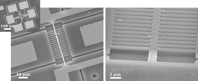
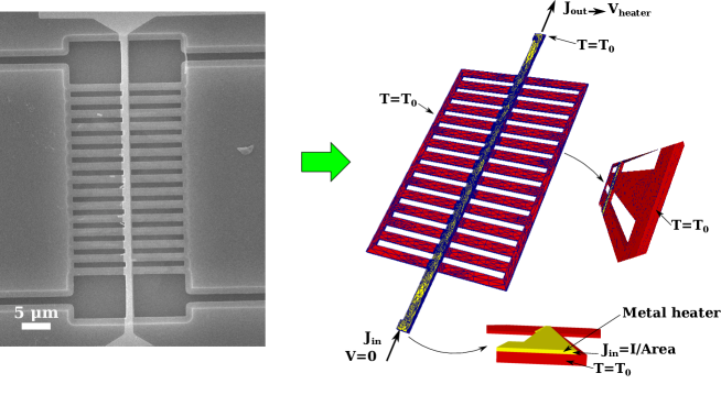
Figure 1 shows SEM images of the typical devices which were used for the 3 measurement of thermal conductivity. The devices are based on monocrystalline silicon ribbons (thin nanomembranes), width a width between 1 and 1.2 m, and a length between 5 and 10 m; the thickness is 240 nm. Our aim is to measure the thermal conductivity in the film plane, parallel to the silicon surface. For this reason, the nanoribbons, arranged in a double-comb configuration, are suspended between the ends of the comb, as seen in the SEM image shown in the right panel. A metal (Gold) track is fabricated, exactly aligned with the center of the comb. This suspended metal resistor acts as the heater for the 3 measurements. Two suspended silicon leads (one at the top and the other at the bottom of the comb) support the metal track, which is connected to the four contacts fabricated on the unsuspended part of the device (see the inset in the left panel of Fig. 1). We summarize the fabrication process, which is a modification of the one that we have already used for the fabrication of silicon nanowire devicesPennelli and Pellegrini (2007); Pennelli et al. (2013). We start from a Silicon On Insulator (SOI) wafer, with a top silicon layer 260 nm thick and a buried oxide layer 2 m thick. A SiO2 layer 40 nm thick is grown at the top, and trenches are defined by means of electron beam lithography, through PMMA resist exposure, development and Buffered Oxide Etch (BHF). The SiO2 layer is then used as a mask for etching the top silicon layer by means of Potassium Hydroxide (KOH etch, 35% in water at 43o C). The trenches are designed for the definition of the comb in the top silicon layer, and for providing electrical and thermal insulation between the different regions of the device. The thickness of the top silicon layer is measured by means of Atomic Force Microscopy (AFM) imaging. To this end, at first the thickness of the SiO2 top layer has been measured by acquiring AFM images of the trenches after the BHF etch and the resist removal by means of acetone. Then, AFM imaging has been repeated after the KOH etch of the Si top layer, assuming that this etch stops at the buried oxide, since it is ineffective on SiO2. In this way, the total thickness of the SiO2 and of the Si top layers has been measured, and the correct thickness of the Si device layer has been obtained by difference. Before the suspension of the nanomembranes, metal tracks and contacts have been fabricated. To this end, an e-beam lithographic step, precisely aligned on the silicon structures, is performed by using a PMMA resist layer. Then, a gold film 70 nm thick is deposited by means of thermal evaporation, and lift-off is performed in hot acetone. Also the exact thickness of the metal film is determined by means of AFM imaging. At this point, the suspension of the silicon nanoribbons, and of the leads for the metal tracks, is obtained by etching the buried oxide which is under the structures (oxide underetching). The nanoribbons have a width between 1 and 1.2 m, therefore more than 10 minutes of BHF etch time is required (etch rate of about 50 nm/min) for the suspension of the comb. As BHF is practically ineffective on Gold, metal tracks and contacts are preserved. The SEM image on the left panel of Fig. 1 shows the silicon nanoribbons organized in a comb configuration. Contacts for the electrical characterization of the central heater, designed in a four probe configuration, are visible in the low magnification SEM image shown in the inset. Two more contacts are provided for the investigation of electrical transport through the silicon nanoribbons. The SEM image shown in the right panel of Fig. 1 includes a cross-section of the device (taken before the fabrication of the heater).
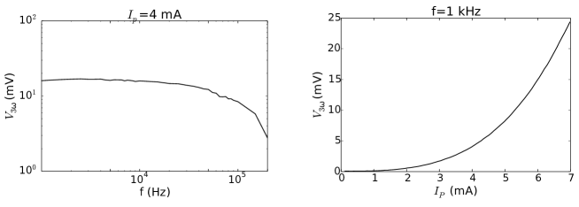
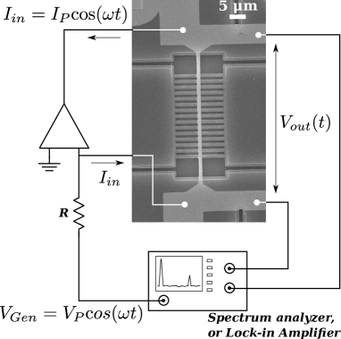
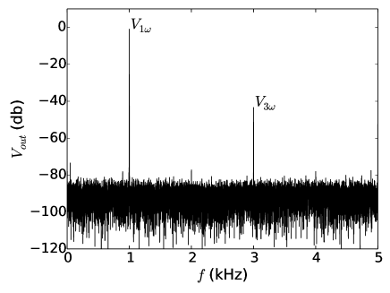
The left panel of Fig. 2 shows the experimental set-up used for the 3 measurements. A sinusoidal current is fed between two (current probes) of the four contacts of the gold track fabricated in the middle of the comb. The voltage is collected through the other two contacts (voltage probes) and measured by means of a lock-in amplifier (Eg&g 5302) which has a differential input amplifier, or by means of a digital signal analyzer. The sinusoidal current signal is obtained from the internal voltage source of the lock-in amplifier (or of the digital signal analyzer), applied to a voltage to current converter (transconductance amplifier), whose schematics is shown in Fig. 2. The internal source provides a voltage signal ); the peak amplitude of the current is . A calibrated resistor of 470 has been used for all the measurements. The measured output impedance of the amplifier is of the order of the G. This value is far larger than the resistance of the heaters for all the measured devices (always in the range between 30 and 300 ). The harmonic distortion of the amplifier has been tested measuring it for several frequencies, up to 1 MHz, by loading the output with a commercial 33 resistor. The lock-in amplifier is locked on the output voltage of its internal source, and the amplitude and phase both of the first and of the third harmonic have been measured. The third harmonic amplitude was always below 10 V, for first harmonic amplitudes as large as 5 V ( V, mA). In the right panel of Fig. 2, we report the spectrum of the output voltage when a sinusoidal current signal, with a frequency of 1 KHz and mA, is applied to the metal heater of a typical device. The presence of a voltage signal (harmonic distortion) whose frequency is three times that of the biasing current is apparent. The measurement of the amplitude of this third harmonic distortion is the basis of the technique. As the injected current is sinusoidal with a frequency , the resulting Joule heating (proportional to the square of the current) has a zero frequency component plus a superimposed 2 component (as a first approximation). The heat generated by the metal track (resistor) for the Joule effect depends on the biasing current and on the resistance value : . This heat must be dissipated through the suspended nanoribbons/nanomembranes. Therefore, the temperature of the resistor, driven by the instantaneous power , depends on the thermal conductivity and on the thermal capacity of the nanomembranes. A measurement of allows to determine the thermal properties ( and ) of the nanomembranes. The temperature of the heater is measured indirectly through the resistance of the metal track. For a reasonably small range of temperature variation, the relationship between and the absolute temperature can be considered linear: , where is a reference temperature, is the resistance at and is a coefficient which depends on the material: K-1 for Gold. Since the temperature of the metal heater oscillates with a frequency 2, as the generated thermal power, the resistance value oscillates with the same frequency. Therefore, the voltage drop between the ends of the heater has a component with an angular frequency 3, since the current varies with a frequency . The amplitude and phase of the 3 component are closely related with the thermal characteristics of the silicon nanoribbons, because the heat generated by the metal resistor/heater must be dissipated through the nanomembranes. We performed two types of measurements as a function of frequency, one with a constant peak amplitude of the bias current, and the other as a function of at a constant frequency. For frequencies smaller than a “transition frequency” , the amplitude of the third harmonic does not depend on the frequency. The transition frequency is proportional to the reciprocal of the propagation time of the heat wave, which depends on the thermal diffusivity coefficient and on the length of the nanomembranes: . In other words, is the penetration depth of a heat wave with frequency . For frequencies , we can assume that the heat wave is in phase with the local temperature, therefore the 3 component of the output voltage is in phase with the biasing current. In this case, the local temperature, and hence the 3 amplitude, depend only on the thermal conductivity . We performed several measurements of the 3 amplitude as a function of the bias current peak amplitude at “sufficiently low” frequencies. Figure 3 reports a measurement on a silicon membrane 240 nm thick.
III Numerical analysis of 3 data
For a precise evaluation of the thermal conductivity from the 3 experimental measurements, a sufficiently refined model of thermal transport in the considered structures must be applied. This is the key point and the most difficult task involved in the application of the 3 technique, because the model must take into account the thermal conductivity, the heat capacity of the material, the electrical conductivity, as well as the geometrical parameters of the device. Standard approaches for the 3 data reduction make some assumptions which can lead to unreliable results, in particular if nanometric structures are considered.
A first approximation is made in the calculation of the generated instantaneous power , for which the value is considered in standard models. If the resistor is biased with a sinusoidal current , can be written as:
The resistor temperature has a sinusoidal variation with a frequency around the average value : , where is the phase of with respect to , and . The metal track resistance becomes:
| (1) |
As a consequence, the measured voltage has a fundamental harmonic with a frequency , whose amplitude and phase depend on the temperature heat and on geometrical factors, and a third harmonic component . With some simple algebra, we obtain:
| (2) |
where is the phase of the third harmonic with respect to the biasing current . The use of the value (at ) for the calculation of the generated instantaneous power is an approximation which holds if the variation of the metal track resistance is very small. Therefore, the models for 3 data reduction developed on the basis of this approximation can be used only when the bias current signal is small. However, in such a case the amplitude of the third harmonic of the measured voltage is in turn very small with respect to that of the first harmonic. The overall voltage signal, including the first and the third harmonic, is applied to the input amplifier of the lock-in, or of the spectrum analyzer. Thus, there is an upper limit for the amplifier gain, which must be chosen in such way as to be compatible with an as linear as possible amplification of the first harmonic. This implies that the measurement of the much smaller third harmonic will be affected by reduced accuracy. A trade-off must therefore be reached between the distortion of the first harmonic and the signal-to-noise ratio achievable for the third harmonic component. A reasonable result was obtained with a first harmonic drive around 0.5 V, corresponding to a third harmonic amplitude in the millivolt range. In this case, the assumption that can be used for the evaluation of can yield unreliable results.
The second approximation considered by standard models, consists in assuming that the heater is very small (of negligible extension) with respect to the size of the structures under test. In this way, an analytical solution of the heat transport equation:
| (3) |
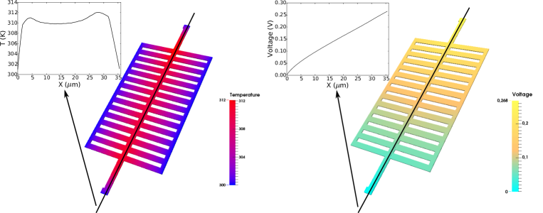
can be found because Joule heating generates a condition on one of the boundaries of the integration domain (where the heater is applied). The heater sets the heat flux : . This second approximation is weak in the case of nanometric devices, because the width of the heater cannot be made very small with respect to that of the structures under test. A third approximation consists in taking into account only the Joule heating of the metal track. This approximation is valid if materials with high electrical resistivity are considered. For this reason, conventional 3 models can be applied only to the measurement of the thermal conductivity of insulating, or semi-insulating, materials. In our case, the metal heater is in contact with the silicon whose thermal conductivity must be measured. The electrical conductivity of silicon is small with respect to that of metal: even if heavily doped silicon is considered (in our case cm-3), its electrical conductivity is several order of magnitude smaller than that of Gold. However, the width and the thickness of the silicon device are larger than those of the metal track: for example, the thickness of the measured nanomembranes is in the range between 120 and 240 nm, while the thickness of the metal heater is always smaller than 70 nm. For this reason, the silicon conductivity must be taken into account for a correct interpretation of the experimental results. In general, the electrical characteristics of the material can be determined with standard techniques, and then the effect of the electrical conductivity can be taken into account considering the full thermoelectric transport equations. In particular, the electrical characteristics of silicon are known in great detail, and both its electrical conductivity and Seebeck coefficient can be determined by means of well-assessed semi-empirical models. However, finding an analytical solution which includes these semi-empirical models could be a very difficult task. We therefore followed a different approach, which is based on the numerical solution of the thermoelectric equations. The technique is more demanding from the computational point of view but it removes all the approximations that need to be taken into account in a practically manageable analytical solution. At first, we obtained the exact shape of the nanoribbons and of the metal track (heater) from a SEM image of the device. The exact thickness of the metal track and of the nanomembranes was measured from AFM images, as explained in the previous section. From this information, a 3D model of the whole device (nanostructures and heater) was generated, as shown in Fig. 4. The figure was drawn over the SEM image shown in the left panel of Fig. 4 by means a vector graphics software, and was saved in a suitable format. Then, a python code was developed to convert the planar figure into a three-dimensional model, taking into account the thicknesses of the structures. At the end, a grid generator software (GMSH) was used for the generation of the mesh. On the basis of this 3D model, it was possible to solve the heat transport equation (Eq. 3) by means of the finite element (FEM) method. However, a very significant computational effort would be required for fitting generic measurements, because transient phenomena should be taken into account and, hence, a very extended data set should be considered. A simpler approach consists in the elaboration of measurements taken in the low frequency regime, in which the local temperature is in phase with the heating power. In this case, the stationary thermal and electrical transport equations can be solved, computing voltages and temperatures as a function of time. The finite element method was used to solve the thermoelectric equations:
combined with the continuity equation for the electrical current and the heat equation:
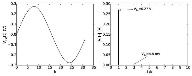
where is the electrical conductivity, is the Seebeck coefficient, is the electric field, is the heat flux, is the thermal conductivity, is the electrical potential, is the absolute temperature. The heat generated by the Joule effect is . The scalar fields and are the unknowns. The 3-D domain includes both the metal (Gold) track and the silicon nanoribbons, which are characterized by different thermoelectric parameters (, and ). For the metal track, Gold parameters were considered. In particular, W/mK; the dependence on temperature of the electrical conductivity was evaluated according to the linear relationship , where K, nm, K-1; the Seebeck coefficient has been assumed to be 5.1 V/K, and it gives a negligible contribution to the thermoelectric transport. For the silicon domain (the nanoribbons), the electrical conductivity was taken into account with the semi-empirical model of AroraArora et al. (1982), which considers both the effect of doping and the temperature dependence; the Slater formula was used to determine the Seebeck coefficient ; the thermal conductivity was used as the fitting parameter (see below). As boundary conditions, the room temperature (Dirichlet boundary condition) has been enforced on the sides of the comb and on the top and bottom faces of the silicon leads (see Fig. 4). Neumann boundary conditions were assumed for the temperature on all the other surfaces. A well-defined current value was assumed in the metal heater through Neumann boundary conditions. For a given value of the current , the boundary condition on each of the two faces at the ends of the metal strip has been , where is the surface of the considered face. The potential was set to 0 on one of the two faces. The potential evaluated in a position close to the other face is the voltage drop between the ends of the metal strip; is the important result of the simulation. The numerical solution of the thermoelectric equations was performed with the FenicsLogg et al. (2012) Python package. Figure 5 shows the temperature and the voltage evaluated for a current mA. In the insets, the profiles of the temperature and of the voltage in the middle of the metal heater (see figure) are shown. The amplitude of the third harmonic component of the output voltage was determined as follows. The sinusoidal current was sampled with a number of points sufficient to reasonably reproduce the waveform (in our case per period): hence, , , where is an integer . For each value of the current the output voltage was determined. The amplitude of the third harmonic was extracted by performing a Discrete Fourier Transform (DFT) of . Figure 6 shows the output voltage for mA (left panel) and its DFT (right panel), where the amplitude both of the first and of the third harmonic is reported. The DFT was performed by means of the FFT module of the numpy Python package. For this plot, a thermal conductivity W/mK was considered.
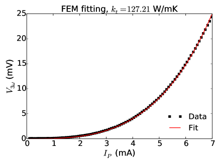
This procedure was used for fitting the experimental curve of the amplitude as a function of the peak current , shown in Figure 7. The thermal conductivity of the nanomembranes was used as a fitting parameter: the amplitude of the third harmonic was computed for all the values of , and was determined by minimizing the sum of the residuals obtained with respect to the experimental points. For the minimization of residuals, a golden section search algorithmPress et al. (1992) was applied. The experimental measurements and the result of the fitting are shown in Fig. 7: a thermal conductivity W/mK was obtained. This value, which is smaller than that of bulk silicon ( W/mK at room temperature), confirms that the thermal conductivity is reduced in nanostructures, as already established by several experimental and theoretical studiesxxx. Our structures can be considered as nanomembranesMarconnet et al. (2013), with a nanometric thickness of nm, and two macroscopic dimensions (1 m wide, 5-10 m long).
IV Comparison with analytical methods
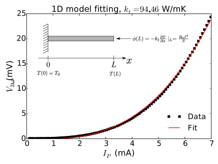
In order to validate our technique, and to evaluate the influence of the approximations needed for the development of an analytic solution on the final result, we used a simple one-dimensional model. We compare the results obtained by fitting the experimental measurements with this model to those obtained with the 3-D FEM model. Each silicon nanoribbon is 1 m wide, 240 nm thick and 7 m long. Therefore, from the geometrical point of view, it can be approximated with a one-dimensional structure whose length is larger than the transverse dimensions. Our typical structure, shown in the SEM image of Fig. 1, is made up of 30 nanoribbons, plus two at the bottom and at the top of the comb needed for routing the electrical signals to the heater. The nanoribbons can be considered in parallel from the thermal point of view, so that the whole structure can be seen as a single rod heated from one side with a power (see the sketch in the inset of Fig. 8).
The heat transport equation 3 can be solved in 1-D, using a Dirichlet boundary condition in (), and a Neumann boundary condition in determined by Joule heating:
| (4) |
where is the total cross section, which is obtained summing all the cross sections of the nanoribbons. The standard approximations of 1) for the evaluation of Joule heating; 2) the width of the heater is negligible; and 3) silicon has a negligible electrical conductivity, while the thermal conductivity of the heater is infinite, were used. The analytical solution can be derived with some simple calculations and reads:
| (5) |
where:
where the imaginary unit has been used. In the low frequency regime, for which:
| (6) |
the expression for becomes:
| (7) |
Therefore, as usual in 3 techniques, the amplitude of the third harmonic turns out to be proportional to the third power of the current peak amplitude, , and to the square of the resistance . The phase is constant and equal to . It is easy to fit this analytical formula to the measurements, using the thermal conductivity as the fitting parameter. Figure 8 shows the fit, using the analytical formula7, of the experimental data, whose fitting with the 3-D FEM model has been reported in Fig. 7. The fit is not as good as that achieved with the 3-D model, and the value of the thermal conductivity W/mK is more than 20% smaller.
V Conclusions
We have presented an approach to the measurement of thermal conductivity of silicon nanostructures based on the technique with the support of a numerical simulation relying on an accurate thermoelectric model. We have pointed out the sources of inaccuracy that result when applying to nanostructures the standard analytical approximations usually associated with the method. Our proposed approach is instead based on a numerical model that includes the solution, by means of a finite element method, of the thermoelectric equations together with the current continuity equation and the heat equation. An automated procedure has been devised to extract a geometrical model of the device from SEM and AFM images. The numerical model has been used to compute the time evolution of the voltage measured in the experiment, with a single fitting parameter, represented by the thermal conductivity, and in particular, to evaluate the amplitude of the third harmonic as a function of the amplitude of the injected current. By comparison with the experimental results, it has then been possible to obtain a good estimate of the thermal conductivity. The very good quality of the fitting of the experimental data (much better that what can be achieved with the existing approximate analytical approaches) is evidence of the validity of the proposed numerical approach, which can be extended to the evaluation of the thermal conductivity of a wide class of nanostructures.
References
- Melosh et al. (2003) N. Melosh, A. Boukay, F. Diana, B. Gerardot, A. Badolato, P. Petroff, and J. Heath, Science 300, 112 (2003).
- Boukay et al. (2008) A. Boukay, Y. Bunimovich, J. Tahir-Kheli, J.-K. Yu, W. A. Goddard III, and J. R. Heat, Nature Letters 451, 168 (2008).
- Park et al. (2011) Y.-H. Park, J. Kim, H. Kim, I. Kim, K. Y. Lee, D. Seo, H. J. Choi, and W. Kim, Applied Physics A 104, 7 (2011).
- Pennelli et al. (2014) G. Pennelli, A. Nannini, and M. Macucci, J. Appl. Phys. 115, 084507 (2014).
- Lim et al. (2012) J. Lim, K. Hippalgaonkar, S. Andrews, C., A. Majumdar, and P. Yang, Nano Letters 12, 2475 (2012).
- Feser et al. (2012) J. Feser, J. Sadhu, B. Azeredo, H. Hsu, J. Ma, J. Kim, M. Seong, N. Fang, X. Li, P. Ferreira, S. Sinha, and D. Cahill, J. Appl. Phys. 112, 114306 (2012).
- Cahill (1990) D. Cahill, Rew. of Scient. Instrum. 61, 802 (1990).
- Choi et al. (2006) T.-Y. Choi, D. Poulikakos, J. Tharian, and U. Sennhauser, Nano Lett. 6, 1589 (2006).
- Lu et al. (2001) L. Lu, W. Yi, and D. Zhang, Rew. of Scient. Instrum. 72, 2996 (2001).
- Jain (2008) K. Jain, A.and Goodson, Journal of Heat Transfer 130, 102404 (2008).
- Pennelli and Pellegrini (2007) G. Pennelli and B. Pellegrini, J. Appl. Phys. 101, 104502 (2007).
- Pennelli et al. (2013) G. Pennelli, M. Totaro, M. Piotto, and P. Bruschi, Nano Lett. 13, 2592 (2013).
- Arora et al. (1982) N. D. Arora, J. R. Hauser, and D. J. Roulston, IEEE transaction on electron devices ED-29, 292 (1982).
- Logg et al. (2012) A. Logg, K. Mardal, and G. Wells, Automated Solution of Differential Equations by the Finite Element Method (Springer Link, 2012).
- Press et al. (1992) W. Press, S. Teukolsky, W. Vettering, and B. Flannery, Numerical Recipes in C (2nd ed,): the art of scientific computing (Cambridge University Press, 1992).
- Mingo (2003) N. Mingo, Physical Review B 68, 1113308 (2003).
- Kazan et al. (2010) M. Kazan, G. Guisbiers, S. Pereira, M. Correia, P. Masri, B. A., S. Volz, and P. Royer, J. of Appl. Phys. 107, 083503 (2010).
- Marconnet et al. (2013) A. Marconnet, M. Asheghi, and K. Goodson, Journal of Heat Transfer 134, 061601 (2013).