Rigid-layer Raman-active modes in -layer Transition Metal Dichalcogenides: interlayer force constants and hyperspectral Raman imaging
Abstract
We report a comparative study of rigid layer Raman-active modes in -layer transition metal dichalcogenides. Trigonal prismatic (2Hc, such as MoSe2, MoTe2, WS2, WSe2) and distorted octahedral (1T’, such as ReS2 and ReSe2) phases are considered. The Raman-active in-plane interlayer shear modes and out-of-plane interlayer breathing modes appear as well-defined features with wavenumbers in the range . These rigid layer modes are well-described by an elementary linear chain model from which the interlayer force constants are readily extracted. Remarkably, these force constants are all found to be of the same order of magnitude. Finally, we show that the prominent interlayer shear and breathing mode features allow high-precision hyperspectral Raman imaging of layer domains within a given transition metal dichalcogenide flake.
Keywords: Transition metal dichalcogenides, two-dimensional materials, rigid-layer phonon modes, interlayer force constants, hyperspectral imaging
![[Uncaptioned image]](/html/1708.01668/assets/TOC.png)
Since the popularization of the mechanical exfoliation technique using adhesive tape 1, the vast family of layered materials (including, graphite, boron nitride, transition metal dichalcogenides (TMDs),…) has attracted tremendous attention. Indeed, mechanical exfoliation and subsequent developments in direct materials growth and transfer methods allow to prepare atomically thin crystals and more recently socalled van der Waals heterostructures 2. Such (quasi) two-dimensional crystals show very different properties from their three-dimensional bulk counterparts, making them ideal candidates for fundamental studies (e.g., dimensionality effects), and for various applications in nanoelectronics, optoelectronics and nanomechanics 3, 4, 5, 6, 7, 8, 9.
In particular, TMDs are well-documented in the bulk state 10, 11 and currently employed for some specific applications, such as dry lubricants in the space industry 12. In particular, semiconducting TMDs hold great promise for the development of innovative optoelectronic devices 4, 7, 8, 13. Single layers of TMDs display exceptional, broadband optoelectronic properties that are distinct from their bulk counterparts 14, 15, together with a valley pseudospin that can be exploited to process information 16, 17. More generally, -layer semiconducting TMDs offer potential advantages (including semi-transparency, low weight, large area, flexibility, strong light-matter interactions, low power consumption and scalability) over most materials currently employed in today’s technologies such as silicon 5, 6, 7, 8. Research in this emerging field rely on swift, local and non-destructive characterization methods, capable of identifying the evolution of the photophysical properties with the number of layers , assessing sample quality and probing interlayer interactions, including in van der Waals heterostructures. In this context, Raman spectroscopy has emerged as a technique of choice to characterize -layer TMDs and to study in details the rich and complex exciton-phonon coupling phenomena 18, 19, 20, 21, 22. In particular, as TMDs are layered compounds, they display low wavenumber ( or equivalently ) interlayer breathing (LBM) and shear modes (LSM). Some of these “rigid layer modes” have already been identified in the bulk crystals decades ago 23. Rigid layer modes are in first approximation insensitive to the intralayer crystal structure, which makes them easier to model theoretically 24. In recent years, the development of ultra-narrow notch filters has greatly facilitated low wavenumber micro-Raman measurements, in particular in two-dimensional materials 25, 26, 27. In TMDs, major outcomes include the experimental determination of the interlayer van der Waals force constants 28, 29, 30, 31, investigation of polytypism and in-plane anisotropy in Rhenium-based TMDs (ReS2, ReSe2) 32, 33, 34, 35, 36, resonant effects 37, 38, 39, 40, as well as investigation of interlayer coupling in van der Waals heterostructures made of two distinct TMD monolayers 41.
In this article, to shed light on the universal behavior of rigid layer Raman modes in TMDs, and more generally in two-dimensional materials, we compare low wavenumber Raman data obtained for six different semiconducting TMDs with diverse optical bandgaps (in the range 1-2 eV) and, importantly, two distinct crystal structures: trigonal prismatic 2Hc molybdenum ditelluride (MoTe2), molybdenum diselenide (MoSe2), tungsten disulfide (WS2) and tungsten diselenide (WSe2), then distorted octohedral 1T’ rhenium disulfide (ReS2) and rhenium diselenide (ReSe2). First, the LSM and LBM are identified as a function of the number of layer for all materials. Then, we describe the evolution of the wavenumbers of the interlayer phonon modes using a simple finite linear chain model allowing us to derive the interlayer force constants. These force constants are found to be of the same order of magnitude for all the materials. Finally, we take advantage of the sub-micrometer resolution offered by micro-Raman spectroscopy and of the existence of well-separated and intense layer rigid modes to report highly accurate hyperspectral imaging of the number of layers in TMD flakes composed of several -layer-thick domains.
1 Methods
-layer TMDs crystals were prepared by mechanical exfoliation of commercially available bulk crystals (2D semiconductors and HQ graphene) onto Si wafers covered with a 90-nm or 285-nm-thick SiO2 epilayer. The number of layers was first estimated from optical contrast and atomic force microscopy measurements, and further characterized using a home-built scanning confocal micro-Raman setup. Micro-Raman scattering studies were carried out in ambient conditions, in a backscattering geometry using high numerical aperture objectives (NA=0.9 for point measurements (see Figs. 1-3) and NA= 0.6 for hyperspectral mapping (Figs. 5-7) and diffraction-limited laser spots). A monochromator equipped with a 2400 grooves/mm holographic grating and coupled to a two-dimensional liquid nitrogen cooled charge-coupled device (CCD) array was used. Linearly polarized laser beams (at photon energies or ) were employed. Spectral resolutions of and were obtained at , , respectively. A laser intensity below was used in order to avoid photoinduced damage of our samples. In order to attain the low wavenumber range, a combination of one narrow bandpass filter and two ultra-narrow notch filters (Optigrate) was used. After optimization, Raman features at wavenumbers as low as 4.5 cm-1 could be measured. Polarized Raman studies are performed using an analyzer placed before the entrance slit of our spectrometer. An achromatic half-wave plate was placed after the analyzer and adequately rotated such that the Raman backscattered beam enters the spectrometer with a fixed polarization. In the following, the sample lies in the plane and light impinges at normal incidence along the direction. Finally, the measured Raman features are fit to Voigt profiles, taking into account the spectral resolution of our apparatus.
2 Structural properties and phonons
TMDs are layered crystals with chemical formula MX2, where M is a transition metal atom (e.g., Mo, W, Ta, Nb, Zr,…) and X is a chalcogen atom (S, Se, Te) 11. These crystals consist in one layer of transition metal atoms sandwiched between two layers of chalcogen atoms, thus forming a X-M-X structure (see Fig. 1). Within each layer, the atoms are held together by strong covalent bonds while adjacent layers are connected by weaker van der Waals interactions. The two most common TMD polytypes are the trigonal prismatic (H) and octahedral (T) structures 11, 42, 43. These terms refer to the metal atom coordinations in the monolayer (see Fig. 1(a) and (b)). For bulk TMDs, these two polytypes are denoted 2H (since two layers are required to form the primitive unit cell) and 1T (as only one layer is required to form the bulk primitive unit cell), respectively.
Here, we focus on 2Hc MoTe2, MoSe2, WS2 and WSe2 (i.e., hexagonal (2H) phase with /BaB AbA/ stacking 43, where upper cases represent chalcogen atoms and lower cases metal atoms) and on 1T ReS2 and ReSe2. More precisely, ReS2 and ReSe2 adopt a distorted octahedral structure (denoted 1T’) with lower symmetry and significant in-plane anisotropy due to covalent bonding between Re atoms leading to quasi one-dimensional Re chains 44, 45, 46, 47. Note that phase transitions between different polytypes can occur, for instance MoS2 crystals can be brought in the metastable 1T/1T’ phase by lithium intercalation and then brought back to the thermodynamic stable 2H phase by deintercalation due to heat 48, 49.
The symmetry analysis of the phonon modes in TMDs has been thoroughly discussed in the literature, see e.g., Refs. 43, 21, 50, 51. In brief, the point group of bulk, odd and even -layer 2Hc TMDs is , and , respectively, while it is for bulk, odd and even -layer 1T’ TMDs. From this analysis, Table 1 summarizes the number of LSM and LBM, their symmetry and their activity for monolayer, bilayer, -layer and bulk 2Hc and 1T’ TMDs.
| Number of layers | 2Hc TMDs | 1T’ TMDs | ||
|---|---|---|---|---|
| LSM | LBM | LSM | LBM | |
| 1 | ||||
| 2 | 2 | |||
| odd | ||||
| even | ||||
| bulk | ||||
3 Identification of the LBM and LSM
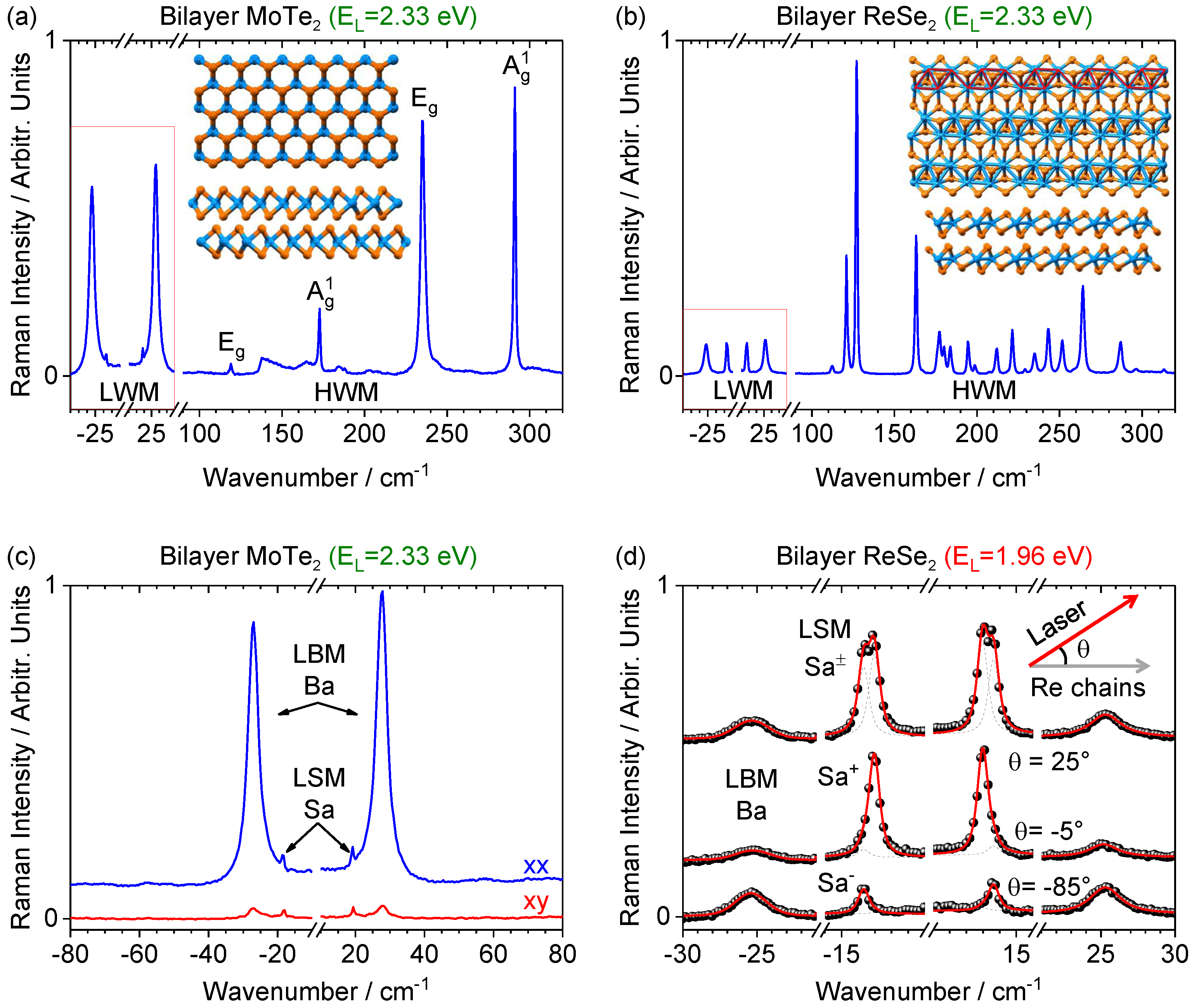
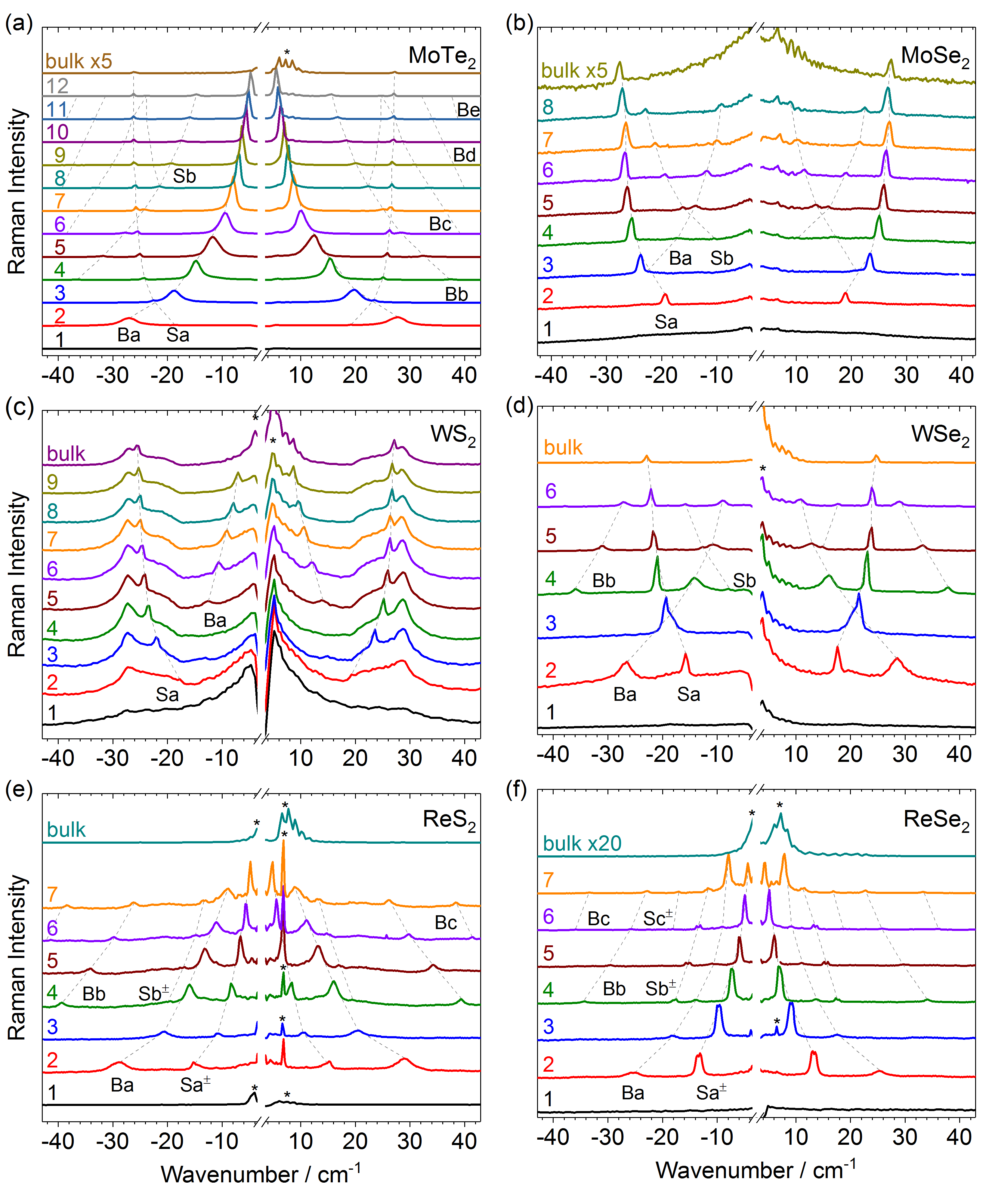
Figure 1 shows typical Raman spectra for bilayer MoTe2 (as a 2Hc compound, see Fig. 1a) and for bilayer ReSe2 (as a 1T’ compound, see Fig. 1b). In the following, we will exclusively discuss the low wavenumber region of the spectrum. In the case of 2Hc TMD bilayers, the LBM and LSM are readily identified by comparing the Raman spectra recorded in the parallel and perpendicular configurations. The LBM (with symmetry) is drastically attenuated in the configuration, whereas the doubly degenerate LSM (with symmetry) has equal intensity in the and configurations (see Fig. 1c). In the case of 1T’ TMD bilayers, both the LSM and LBM have symmetry and display non-trivial dependence on the polarization conditions. By carefully rotating the sample relative to the fixed laser polarization and recording the Raman spectra in the configuration, it is possible to spectrally resolve the splitting between the two LSM that arises due to in-plane anisotropy (see Fig. 1d and Ref. 34).
Figure 2 display low wavenumber Raman spectra as a function of for six different TMDs. All spectra in this figure were recorded at . As in previous reports 28, 29, 30, 31, for , one can clearly identify the previously reported branches of LBM and LSM modes, whose wavenumber vary significantly with . The LSM and LBM branches are identified using polarized measurements as described above and are denoted Ba, Bb,…and Sa, Sb,…(Sa±, Sb± for ReS2 and ReSe2, where the subscript denotes the two split LSM features), respectively (see Fig. 3). As further discussed below, the absolute and relative intensities of the LSM and LBM vary largely depending on the material and on (not shown), suggesting pronounced resonance Raman effects. Remarkably, in the case of WS2, a prominent mode appears near , irrespective of . This feature, also previously seen in MoS2 layers 53 has tentatively been assigned to a higher order resonant Raman process involving finite momentum transverse acoustic (TA) phonons and electron-defect scattering, such that energy and momentum are conserved 40.
4 Finite linear chain model
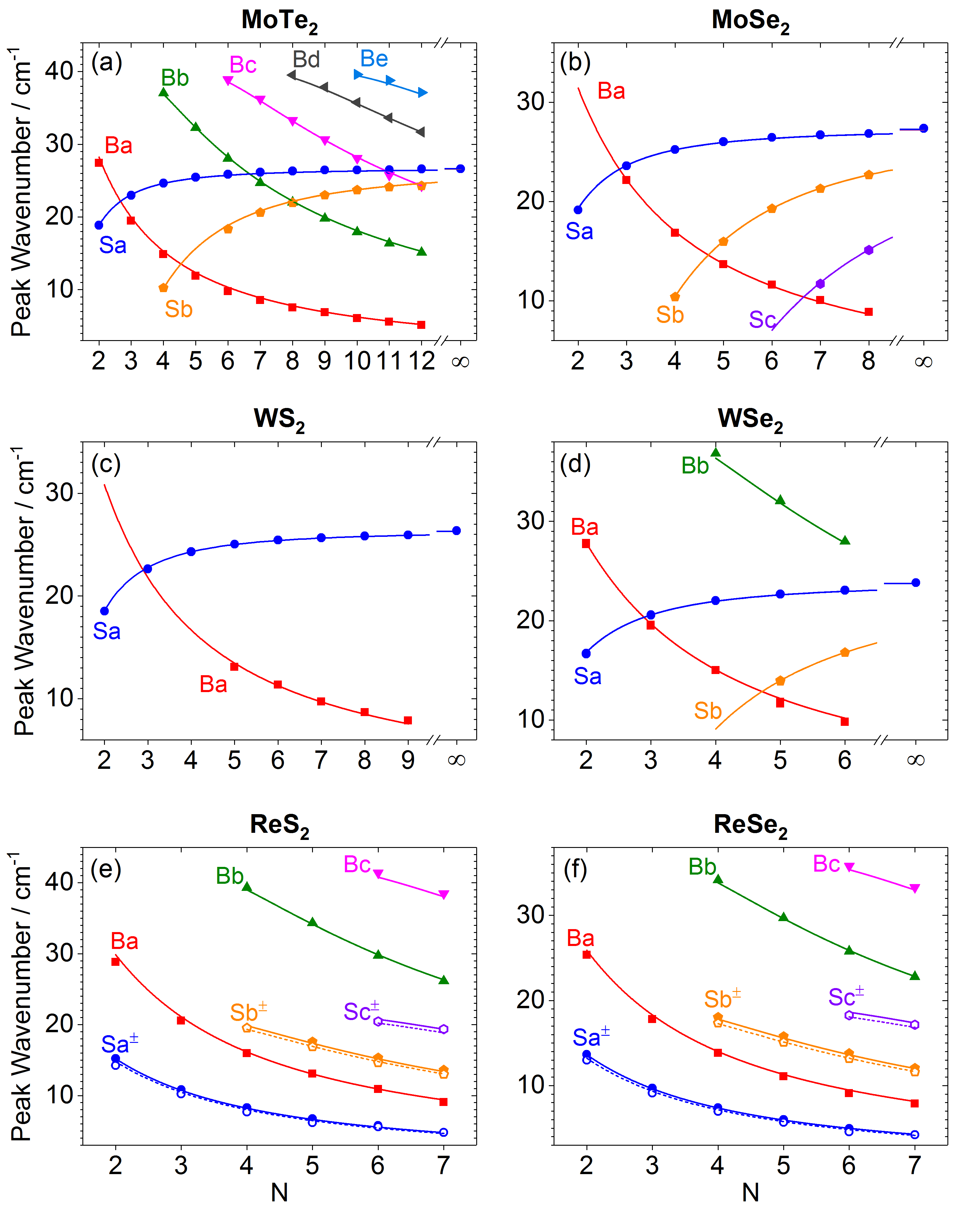
The wavenumbers of the LSM and LBM are displayed in Fig. 3. The evolution of these wavenumbers with can be derived using density functional theory (DFT) 29, 30 or analytically, by diagonalizing the dynamical matrix 24, 28. In the case of interlayer modes, we can use a finite linear chain model 54, in which each layer is treated as a rigid mass unit with a mass , where is the mass per unit area of the chalcogen atom and of the metal atom, to derive the dynamical matrix. Applying this model to a -layer sample and diagonalizing the dynamical matrix leads to the normal modes of this system, where the displacement of the i layer plane () is with the eigenwavenumbers and eigenvectors :
| (1) | |||||
| (4) |
where is the interlayer force constant and denotes the speed of light. Note that corresponds to the acoustic mode with a zero wavenumber and a center of mass not at rest. For , the non-zero wavenumber is and for the bulk wavenumber . These two expressions can be deduced from simple considerations. For , the problem is equivalent to a spring-mass system with a reduced mass and a spring . Such an oscillator has an eigenwavenumber . For the bulk, the two masses are connected by two springs of stiffness because of the periodic boundary conditions. This system is equivalent to one oscillator with a reduced mass and a spring constant which wavenumber is .
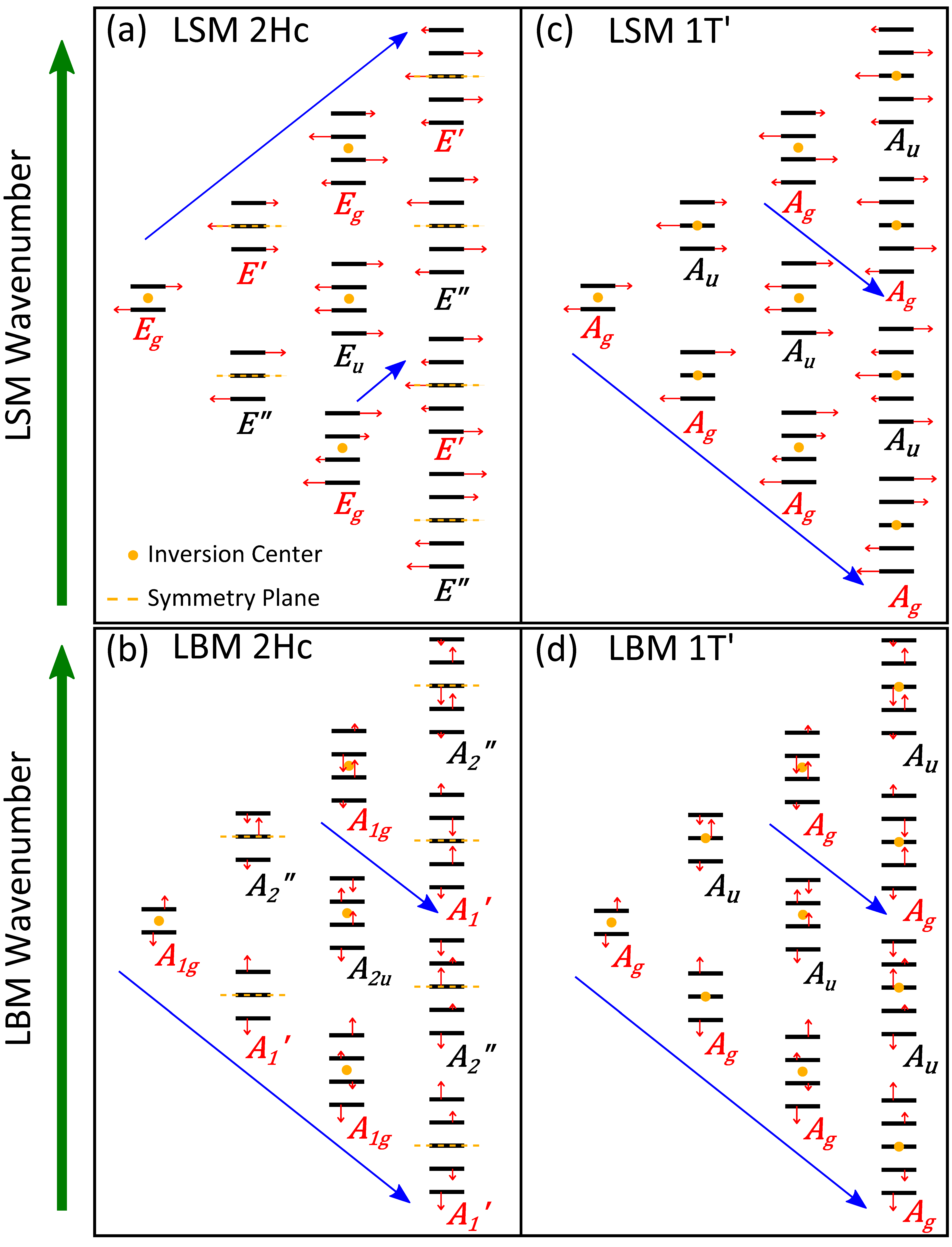
Using Eq. (1), we globally fit the LSM and LBM branches with the shear () and breathing () force constants as the only fitting parameters. The LSM and LBM normal displacements are represented in Fig. 4 up to . Remarkably, for 2Hc TMDs, the experimentally observed Raman-active LSM Sa, Sb, Sc, …(resp. LBM Ba, Bb, Bc, …) correspond to branches (resp. ) in Eq. (1), with increasing (resp. decreasing) wavenumber as augments. In contrast, for 1T’ TMDs, both LSM Sa±, Sb±, Sc±, … and LBM Ba, Bb, Bc, …wavenumbers decrease as increases and correspond to branches in Eq. (1). These contrasting behaviors have previously been rationalized using a symmetry analysis (see Fig. 4 and Ref. 34). More generally, there is no straightforward connection between the Raman activity (determined by the crystal symmetries) and the measured Raman intensity of a given Raman-active mode. For example, it has been shown that the most intense experimentally observed LBM in bernal-stacked and twisted -layer graphene correspond to (Ref. 55) and (Ref. 56) in Eq. (1), respectively.
Eq. (1) provides an excellent fit to our data for all materials (see Fig. 3). This result demonstrates that higher-order nearest neighbor interactions 20, 31 can be neglected when describing rigid layer modes. The extracted force constants are reported in Table 2 and compared to measurements on other layered materials found in the literature. Despite different compounds and crystal structure, we notice that the interlayer force constant are all very close. This conclusion is not surprising for 2Hc compounds. However, since the evolution of the optical properties of ReS2 and ReSe2 with varying are not as pronounced as in the case of MoX2 and WX2, it has been suggested that the layers that compose a ReX2 stack might be weakly coupled 57. Low wavenumber Raman measurements rather demonstrate that ReX2 should be considered as van der Waals materials with similar interlayer coupling as 2Hc TMDs 32, 33, 34, 35, 36. Let us also note that polytypism (as observed in MoS2 58 and ReS2 35, 36) imply that stacking order with different symmetries may lead to slightly different force constants and fan diagrams for the rigid layer modes.
| Material | ||
|---|---|---|
| MoTe2 (Ref. 31 and this work) | 34.2 | 76.9 |
| MoTe2 (Ref. 59, 60) | 36.0, 42.5 | 75.0, 91.2 |
| MoSe2 (this work) | 29.6 | 78.4 |
| MoSe2 (Ref. 39) | 29.2 | 87.3 |
| WS2 (this work) | 29.4 | 80.6 |
| WSe2 (this work) | 30.5 | 83.7 |
| WSe2 29 | 30.7 | 86.3 |
| ReS2 (Ref. 34 and this work) | 17.1/18.9 | 69.3 |
| ReSe2 (Ref. 34 and this work) | 17.8/19.4 | 69.2 |
| MoS2 (Ref. 30, 28, 29) | 28.1, 28.2, 27.2 | 88.1, 89.0, 86.2 |
| Graphite (Ref. 25, 55) | 12.8 | 88.0 |
To close this section, we provide an alternative description of rigid-layer phonon modes in -layer crystals using the bulk phonon dispersion relation 61, 24. This description can be viewed as a “top-down” approach, as opposed to a “bottom-up” description outlined above. The dispersion relation of an infinite monoatomic linear chain of lattice parameter is given by 62
| (5) |
where is the phonon wavevector taken in the Brillouin zone of the monoatomic linear chain. However, Eq. (5) is not the dispersion relation of the bulk crystal since the unit cell contains two layers. Nevertheless, it can be deduced from Eq. (5) knowing that the size of the Brillouin zone changes from to . Hence the dispersion relation of the bulk crystal is
| (6) |
with . The phonon branch with the () corresponds to the optical (acoustic) branch. Note that gives the two wavenumbers of the bulk zone center phonon modes. For non-zero wavevector and 111For , and thus the only mode is the acoustic one., comparing Eqs. (1) and (6) yield
| (7) |
with and . Thus, we find that the LSM and LBM of the -layer system are obtained through vertical cuts in the bulk dispersion at quantized values given by Eq. (7), in the range 222Similar results could be obtain in the range since the dispersion relation is an even function of .. Interestingly, Eq. (7) suggests that the modes are confined to an effective thickness of . Extrapolating to the single layer gives an effective thickness of (i.e., an interplanar distance) for one layer, as it is assumed in the literature 63, 64, e.g. for multiple reflection calculations involving layered crystals. Let us finally note that the linear chain model outlined above can be generalized to provide a complete description of all the phonon modes in a -Layer system 20, 31.
5 Hyperspectral Raman imaging
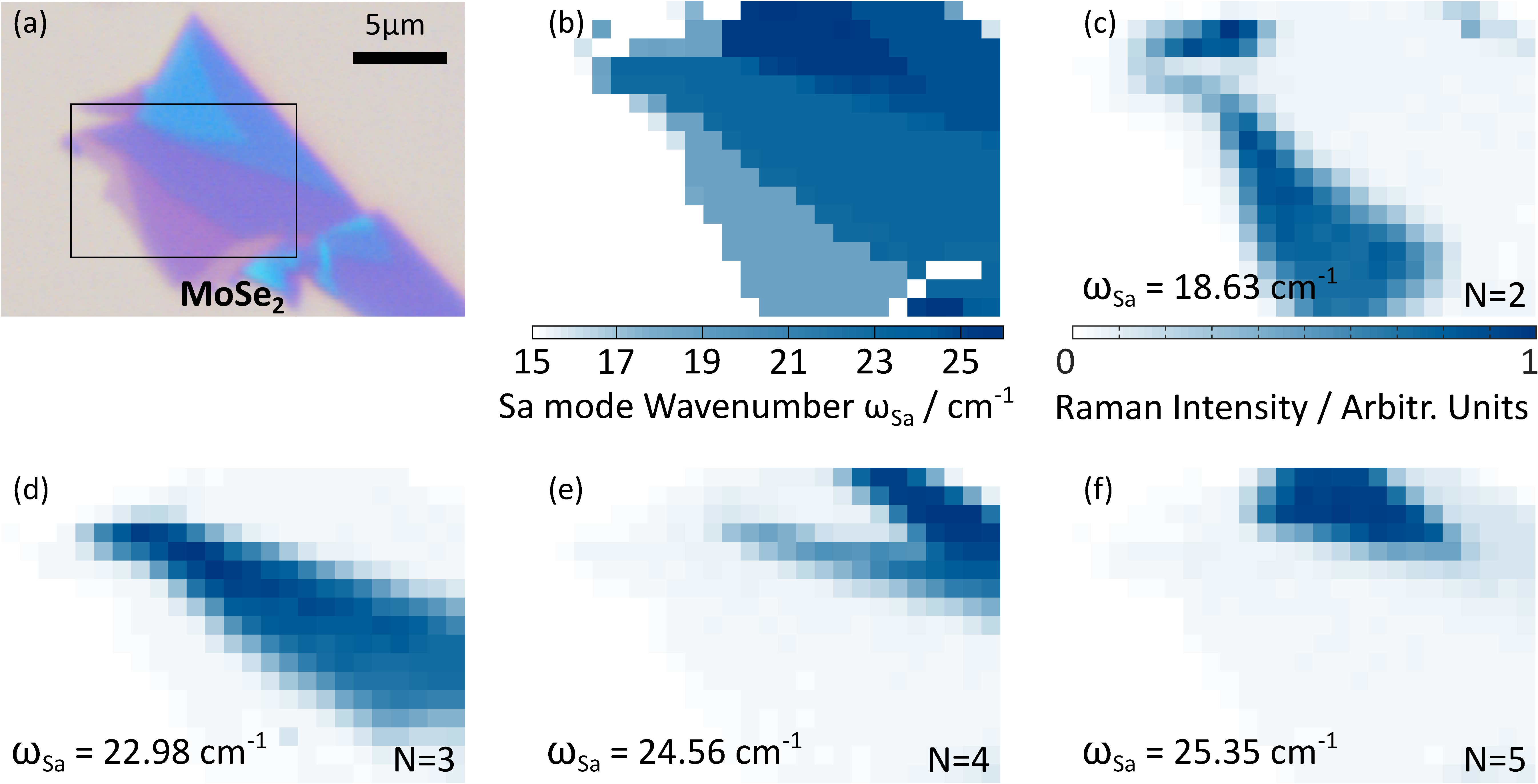
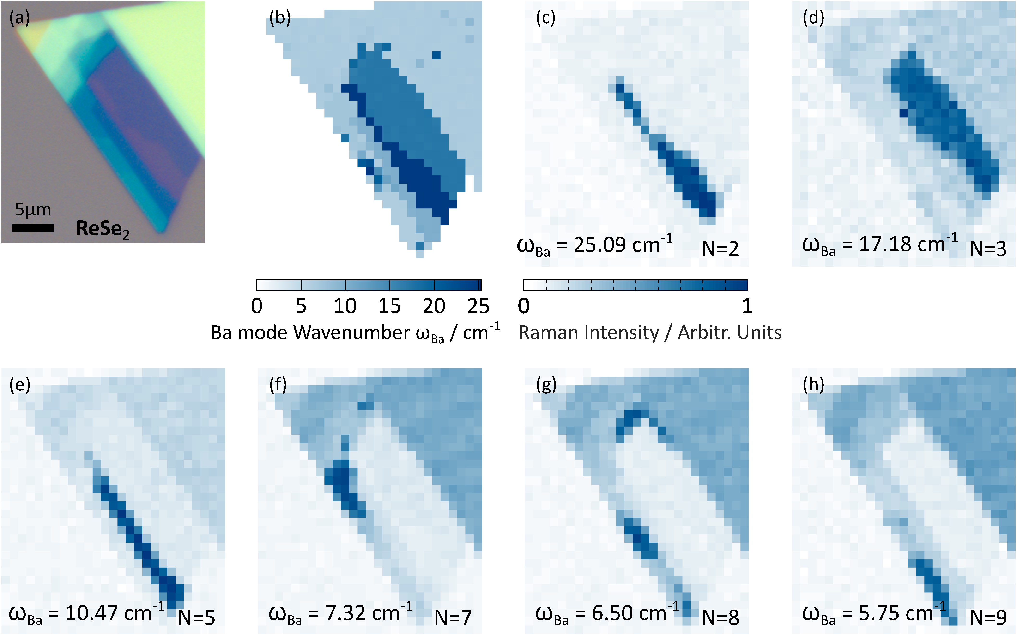
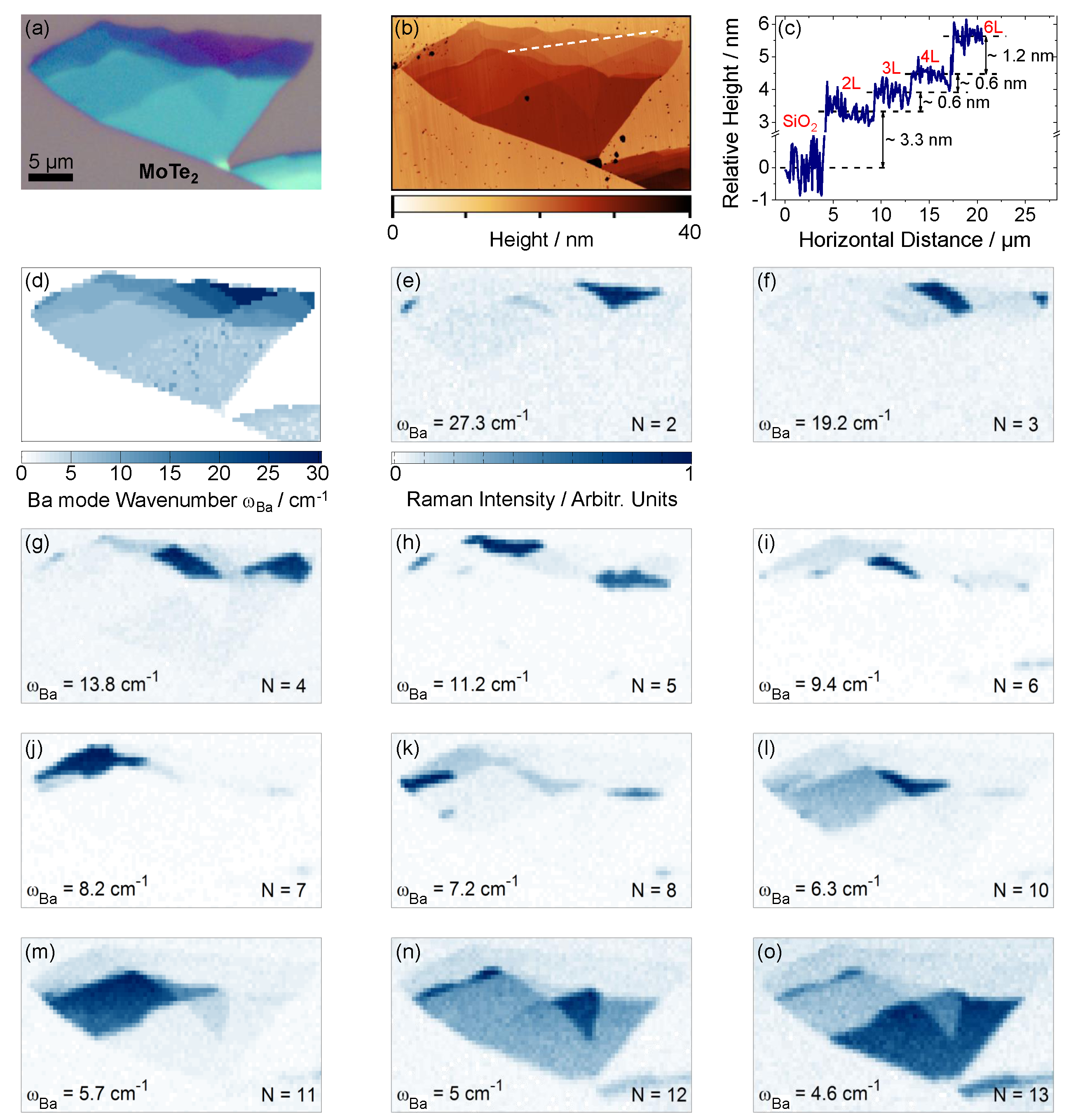
The observation of a well-defined, -dependent series of LSM and LBM opens very interesting perspectives for hyperspectral Raman imaging. In Fig. 5(a), we present an optical image of a MoTe2 crystal containing domains with ranging from to . The number of layers is readily identified by atomic force microscopy (Fig. 5(b)) and the height difference between two MoTe2 layers is measured to be , in agreement with previous studies 65, 66, 67, 68. Note that the step between the Si/SiO2 substrate and might be due to changes in the tip-surface interaction between the substrate and the sample 69 or to the presence of adsorbates under the sample 18.
In Fig. 5(c), we plot the hyperspectral map of the wavenumber of the lowest energy and most intense LBM (see Fig. 3). This map readily allows one to distinguish -layer domains, up to with a high contrast. One can also map out the Raman scattered intensity at a given shift. By selecting the Raman shifts that correspond to the Ba mode wavenumber of a -layer specimen, we can then selectively image all the -layer domains with an unprecedented contrast as illustrated in Fig. 5(d)-(o). Such a high contrast arises chiefly from the strong enhancement of the LBM features (especially for the Ba branch) and to the fact that the Ba branch is spectrally well separated from the other LBM and LSM modes.
6 Conclusion and outlook
We have reviewed the rigid layer shear and breathing modes in layer semiconducting transition metal dichalcogenides in the 2Hc and 1T’ phases. Owing to the strong light matter-interactions in these materials, optical excitation above the optical bandgap leads to intense and rather easily measurable rigid-layer Raman features. The latter are well-separated and are very well-modeled using an elementary one-dimensional linear chain model, from which interlayer in-plane and out-of-plane force constants in the range and interlayer breathing force constants in the range are extracted. In particular, we note that for a given material, the wavenumber of the rigid layer mode show marginal sample-to-sample variation and no surface effects have to be considered to describe the rigid layer modes in substrate-supported samples.
This article has essentially focused on the well-defined wavenumbers of the rigid layer modes. A highly stimulating direction now consists in describing the dramatic changes in the integrated intensities of the rigid layer modes. Recent Raman scattering studies using a broad range of laser photon energies have uncovered non-trivial resonant effects (see also review by Lee and Cheong in this special issue). Such resonance effects may in part be directly connected with the excitonic manifold 70, 71, 72 of a given material and the symmetries of the phonon modes 73, 74, 75, 37, 39, 38, 60, 76, 40. However, quantum interference effects may largely affect the Raman intensity at a given laser photon energy in a non-intutive fashion 22. In the particular case of in-plane anisotropic materials, coupling between anisotropic excitons 77, 78 and complex phonon manifolds 51, 50 result in even more complicated polarization-dependent Raman responses 34, 79, 80. All these observations show that there is still room for innovative theoretical and experimental efforts in order to provide a comprehensive description of exciton-phonon coupling in transition metal dichalcogenides and related layered materials.
We are grateful to H. Majjad for help with AFM measurements, to the StNano clean room staff for technical assistance. We acknowledge financial support from the Agence Nationale de la Recherche (under grant H2DH ANR-15-CE24-0016) and from the LabEx NIE (Under Grant ANR-11-LABX-0058-NIE). S.B. is a member of Institut Universitaire de France (IUF).
References
- Novoselov et al. 2005 Novoselov, K.; Jiang, D.; Schedin, F.; Booth, T.; Khotkevich, V.; Morozov, S.; Geim, A. Proc. Natl. Acad. Sci. U.S.A. 2005, 102, 10451–10453
- Novoselov et al. 2016 Novoselov, K.; Mishchenko, A.; Carvalho, A.; Neto, A. C. Science 2016, 353, aac9439
- Castro Neto et al. 2009 Castro Neto, A. H.; Guinea, F.; Peres, N. M. R.; Novoselov, K. S.; Geim, A. K. Rev. Mod. Phys. 2009, 81, 109–162
- Koppens et al. 2014 Koppens, F.; Mueller, T.; Avouris, P.; Ferrari, A.; Vitiello, M.; Polini, M. Nat. Nanotechnol. 2014, 9, 780–793
- Akinwande et al. 2014 Akinwande, D.; Petrone, N.; Hone, J. Nat. Commun. 2014, 5, 6678
- Wang et al. 2012 Wang, Q. H.; Kalantar-Zadeh, K.; Kis, A.; Coleman, J. N.; Strano, M. S. Nat. Nanotechnol. 2012, 7, 699–712
- Xia et al. 2014 Xia, F.; Wang, H.; Xiao, D.; Dubey, M.; Ramasubramaniam, A. Nat. Photonics 2014, 8, 899–907
- Mak and Shan 2016 Mak, K. F.; Shan, J. Nat. Photonics 2016, 10, 216–226
- Castellanos-Gomez et al. 2015 Castellanos-Gomez, A.; Singh, V.; van der Zant, H. S. J.; Steele, G. A. Ann. Phys. 2015, 527, 27–44
- Frindt and Yoffe 1963 Frindt, R.; Yoffe, A. Physical properties of layer structures: optical properties and photoconductivity of thin crystals of molybdenum disulphide. Proceedings of the Royal Society of London A: Mathematical, Physical and Engineering Sciences. 1963; pp 69–83
- Wilson and Yoffe 1969 Wilson, J.; Yoffe, A. Adv. Phys. 1969, 18, 193–335
- Hilton and Fleischauer 1992 Hilton, M. R.; Fleischauer, P. D. Surf. Coat. Technol. 1992, 54, 435–441
- Mueller 2016 Mueller, T. 2D Materials for Nanoelectronics 2016, 17, 241
- Mak et al. 2010 Mak, K. F.; Lee, C.; Hone, J.; Shan, J.; Heinz, T. F. Phys. Rev. Lett. 2010, 105, 136805
- Splendiani et al. 2010 Splendiani, A.; Sun, L.; Zhang, Y.; Li, T.; Kim, J.; Chim, C.-Y.; Galli, G.; Wang, F. Nano Lett. 2010, 10, 1271–1275
- Xu et al. 2014 Xu, X.; Yao, W.; Xiao, D.; Heinz, T. F. Nat. Phys. 2014, 10, 343–350
- Schaibley et al. 2016 Schaibley, J. R.; Yu, H.; Clark, G.; Rivera, P.; Ross, J. S.; Seyler, K. L.; Yao, W.; Xu, X. Nature Reviews Materials 2016, 1, 16055
- Lee et al. 2010 Lee, C.; Yan, H.; Brus, L. E.; Heinz, T. F.; Hone, J.; Ryu, S. ACS Nano 2010, 4, 2695–2700
- Molina-Sánchez and Wirtz 2011 Molina-Sánchez, A.; Wirtz, L. Phys. Rev. B 2011, 84, 155413
- Luo et al. 2013 Luo, X.; Zhao, Y.; Zhang, J.; Xiong, Q.; Quek, S. Y. Phys. Rev. B 2013, 88, 075320
- Zhang et al. 2015 Zhang, E.; Jin, Y.; Yuan, X.; Wang, W.; Zhang, C.; Tang, L.; Liu, S.; Zhou, P.; Hu, W.; Xiu, F. Adv. Func. Mater. 2015, 25, 4076–4082
- Miranda et al. 2017 Miranda, H. P. C.; Reichardt, S.; Froehlicher, G.; Molina-Sánchez, A.; Berciaud, S.; Wirtz, L. Nano Lett. 2017, 17, 2381–2388
- Wieting et al. 1980 Wieting, T.; Grisel, A.; Levy, F. Physica B+ C 1980, 99, 337–342
- Michel and Verberck 2012 Michel, K. H.; Verberck, B. Phys. Rev. B 2012, 85, 094303
- Tan et al. 2012 Tan, P. H.; Han, W. P.; Zhao, W. J.; Wu, Z. H.; Chang, K.; Wang, H.; Wang, Y. F.; Bonini, N.; Marzari, N.; Pugno, N. Nat. Mater. 2012, 11, 294–300
- Plechinger et al. 2012 Plechinger, G.; Heydrich, S.; Eroms, J.; Weiss, D.; Schüller, C.; Korn, T. Appl. Phys. Lett. 2012, 101, 101906
- Zeng et al. 2012 Zeng, H.; Zhu, B.; Liu, K.; Fan, J.; Cui, X.; Zhang, Q. M. Phys. Rev. B 2012, 86, 241301
- Zhang et al. 2013 Zhang, X.; Han, W. P.; Wu, J. B.; Milana, S.; Lu, Y.; Li, Q. Q.; Ferrari, A. C.; Tan, P. H. Phys. Rev. B 2013, 87, 115413
- Zhao et al. 2013 Zhao, Y.; Luo, X.; Li, H.; Zhang, J.; Araujo, P. T.; Gan, C. K.; Wu, J.; Zhang, H.; Quek, S. Y.; Dresselhaus, M. S.; Xiong, Q. Nano Lett. 2013, 13, 1007–1015
- Boukhicha et al. 2013 Boukhicha, M.; Calandra, M.; Measson, M.-A.; Lancry, O.; Shukla, A. Phys. Rev. B 2013, 87, 195316
- Froehlicher et al. 2015 Froehlicher, G.; Lorchat, E.; Fernique, F.; Joshi, C.; Molina-Sánchez, A.; Wirtz, L.; Berciaud, S. Nano Lett. 2015, 15, 6481–6489
- Zhao et al. 2015 Zhao, H.; Wu, J.; Zhong, H.; Guo, Q.; Wang, X.; Xia, F.; Yang, L.; Tan, P.; Wang, H. Nano Res. 2015, 8, 3651–3661
- Nagler et al. 2015 Nagler, P.; Plechinger, G.; Schüller, C.; Korn, T. Phys. Status Solidi RRL 2015, 185–189
- Lorchat et al. 2016 Lorchat, E.; Froehlicher, G.; Berciaud, S. ACS Nano 2016, 10, 2752––2760, 10.1021/acsnano.5b07844
- He et al. 2016 He, R.; Yan, J.-A.; Yin, Z.; Ye, Z.; Ye, G.; Cheng, J.; Li, J.; Lui, C. H. Nano Lett. 2016, 16, 1404–1409
- Qiao et al. 2016 Qiao, X.-F.; Wu, J.-B.; Zhou, L.; Qiao, J.; Shi, W.; Chen, T.; Zhang, X.; Zhang, J.; Ji, W.; Tan, P.-H. Nanoscale 2016, 8, 8324–8332
- Lee et al. 2015 Lee, J.-U.; Kim, K.; Cheong, H. 2D Mater. 2015, 2, 044003
- Soubelet et al. 2016 Soubelet, P.; Bruchhausen, A. E.; Fainstein, A.; Nogajewski, K.; Faugeras, C. Phys. Rev. B 2016, 93, 155407
- Kim et al. 2016 Kim, K.; Lee, J.-U.; Nam, D.; Cheong, H. ACS Nano 2016, 10, 8113–8120
- Tan et al. 2017 Tan, Q.-H.; Sun, Y.-J.; Liu, X.-L.; Zhao, Y.; Xiong, Q.; Tan, P.-H.; Zhang, J. arXiv preprint arXiv:1704.01315 2017,
- Lui et al. 2015 Lui, C. H.; Ye, Z.; Ji, C.; Chiu, K.-C.; Chou, C.-T.; Andersen, T. I.; Means-Shively, C.; Anderson, H.; Wu, J.-M.; Kidd, T.; Lee, Y.-H.; He, R. Phys. Rev. B 2015, 91, 165403
- Katzke et al. 2004 Katzke, H.; Tolédano, P.; Depmeier, W. Phys. Rev. B 2004, 69, 134111
- Ribeiro-Soares et al. 2014 Ribeiro-Soares, J.; Almeida, R. M.; Barros, E. B.; Araujo, P. T.; Dresselhaus, M. S.; Cançado, L. G.; Jorio, A. Phys. Rev. B 2014, 90, 115438
- Ho et al. 1997 Ho, C. H.; Liao, P. C.; Huang, Y. S.; Yang, T. R.; Tiong, K. K. J. Appl. Phys. 1997, 81, 6380–6383
- Ho et al. 1998 Ho, C. H.; Huang, Y. S.; Tiong, K. K.; Liao, P. C. Phys. Rev. B 1998, 58, 16130–16135
- Ho et al. 2004 Ho, C. H.; Lee, H. W.; Wu, C. C. J. Phys.: Condens. Matter 2004, 16, 5937
- Tiong et al. 1999 Tiong, K.; Ho, C.; Huang, Y. Solid State Commun. 1999, 111, 635 – 640
- Kappera et al. 2014 Kappera, R.; Voiry, D.; Yalcin, S. E.; Branch, B.; Gupta, G.; Mohite, A. D.; Chhowalla, M. Nat. Mater. 2014, 13, 1128–1134
- Guo et al. 2015 Guo, Y.; Sun, D.; Ouyang, B.; Raja, A.; Song, J.; Heinz, T. F.; Brus, L. E. Nano Lett. 2015, 15, 5081–5088
- Wolverson et al. 2014 Wolverson, D.; Crampin, S.; Kazemi, A. S.; Ilie, A.; Bending, S. J. ACS Nano 2014, 8, 11154
- Feng et al. 2015 Feng, Y.; Zhou, W.; Wang, Y.; Zhou, J.; Liu, E.; Fu, Y.; Ni, Z.; Wu, X.; Yuan, H.; Miao, F.; Wang, B.; Wan, X.; Xing, D. Phys. Rev. B 2015, 92, 054110
- Loudon 1964 Loudon, R. Adv. Phys. 1964, 13, 423
- Lee et al. 2015 Lee, J.-U.; Park, J.; Son, Y.-W.; Cheong, H. Nanoscale 2015, 7, 3229–3236
- Luo et al. 1996 Luo, N. S.; Ruggerone, P.; Toennies, J. P. Phys. Rev. B 1996, 54, 5051–5063
- Lui et al. 2014 Lui, C. H.; Ye, Z.; Keiser, C.; Xiao, X.; He, R. Nano Lett. 2014, 14, 4615–4621
- Wu et al. 2015 Wu, J.-B.; Hu, Z.-X.; Zhang, X.; Han, W.-P.; Lu, Y.; Shi, W.; Qiao, X.-F.; Ijiäs, M.; Milana, S.; Ji, W.; Ferrari, A. C.; Tan, P.-H. ACS Nano 2015, 9, 7440–7449
- Tongay et al. 2014 Tongay, S. et al. Nat. Commun. 2014, 5, 3252
- Lee et al. 2016 Lee, J.-U.; Kim, K.; Han, S.; Ryu, G. H.; Lee, Z.; Cheong, H. ACS Nano 2016, 10, 1948–1953
- Grzeszczyk et al. 2016 Grzeszczyk, M.; Gołasa, K.; Zinkiewicz, M.; Nogajewski, K.; Molas, M. R.; Potemski, M.; Wysmołek, A.; Babiński, A. 2D Mater. 2016, 3, 025010
- Song et al. 2016 Song, Q. J.; Tan, Q. H.; Zhang, X.; Wu, J. B.; Sheng, B. W.; Wan, Y.; Wang, X. Q.; Dai, L.; Tan, P. H. Phys. Rev. B 2016, 93, 115409
- Karssemeijer and Fasolino 2011 Karssemeijer, L.; Fasolino, A. Surf. Sci. 2011, 605, 1611–1615
- Ashcroft and Mermin 1976 Ashcroft, N. W.; Mermin, N. D. Solid state physics; Holt, Rinehart and Winston, 1976
- Yoon et al. 2009 Yoon, D.; Moon, H.; Son, Y.-W.; Choi, J. S.; Park, B. H.; Cha, Y. H.; Kim, Y. D.; Cheong, H. Phys. Rev. B 2009, 80, 125422
- Li et al. 2012 Li, S.-L.; Miyazaki, H.; Song, H.; Kuramochi, H.; Nakaharai, S.; Tsukagoshi, K. ACS Nano 2012, 6, 7381–7388
- Böker et al. 2001 Böker, T.; Severin, R.; Müller, A.; Janowitz, C.; Manzke, R.; Voß, D.; Krüger, P.; Mazur, A.; Pollmann, J. Phys. Rev. B 2001, 64, 235305
- Ruppert et al. 2014 Ruppert, C.; Aslan, O. B.; Heinz, T. F. Nano Lett. 2014, 14, 6231–6236
- Yamamoto et al. 2014 Yamamoto, M.; Wang, S. T.; Ni, M.; Lin, Y.-F.; Li, S.-L.; Aikawa, S.; Jian, W.-B.; Ueno, K.; Wakabayashi, K.; Tsukagoshi, K. ACS Nano 2014, 8, 3895–3903
- Lezama et al. 2015 Lezama, I. G.; Arora, A.; Ubaldini, A.; Barreteau, C.; Giannini, E.; Potemski, M.; Morpurgo, A. F. Nano Lett. 2015, 15, 2336–2342
- Nemes-Incze et al. 2008 Nemes-Incze, P.; Osváth, Z.; Kamarás, K.; Biró, L. Carbon 2008, 46, 1435–1442
- Chernikov et al. 2014 Chernikov, A.; Berkelbach, T. C.; Hill, H. M.; Rigosi, A.; Li, Y.; Aslan, O. B.; Reichman, D. R.; Hybertsen, M. S.; Heinz, T. F. Phys. Rev. Lett. 2014, 113, 076802
- Wang et al. 2015 Wang, G.; Marie, X.; Gerber, I.; Amand, T.; Lagarde, D.; Bouet, L.; Vidal, M.; Balocchi, A.; Urbaszek, B. Phys. Rev. Lett. 2015, 114, 097403
- Li et al. 2014 Li, Y.; Chernikov, A.; Zhang, X.; Rigosi, A.; Hill, H. M.; van der Zande, A. M.; Chenet, D. A.; Shih, E.-M.; Hone, J.; Heinz, T. F. Phys. Rev. B 2014, 90, 205422
- Carvalho et al. 2016 Carvalho, B. R.; Malard, L. M.; Alves, J. M.; Fantini, C.; Pimenta, M. A. Phys. Rev. Lett. 2016, 116, 089904
- Scheuschner et al. 2015 Scheuschner, N.; Gillen, R.; Staiger, M.; Maultzsch, J. Phys. Rev. B 2015, 91, 235409
- Zhang et al. 2015 Zhang, X.; Qiao, X.-F.; Shi, W.; Wu, J.-B.; Jiang, D.-S.; Tan, P.-H. Chem. Soc. Rev. 2015, 44, 2757
- del Corro et al. 2016 del Corro, E.; Botello-Méndez, A.; Gillet, Y.; Elias, A. L.; Terrones, H.; Feng, S.; Fantini, C.; Rhodes, D.; Pradhan, N.; Balicas, L.; Gonze, X.; Charlier, J.-C.; Terrones, M.; Pimenta, M. A. Nano Lett. 2016, 16, 2363–2368
- Aslan et al. 2016 Aslan, O. B.; Chenet, D. A.; van der Zande, A. M.; Hone, J. C.; Heinz, T. F. ACS Photonics 2016, 3, 96–101
- Arora et al. 2017 Arora, A.; Noky, J.; Drüppel, M.; Jariwala, B.; Deilmann, T.; Schneider, R.; Schmidt, R.; Del Pozo-Zamudio, O.; Stiehm, T.; Bhattacharya, A.; Krüger, P.; Michaelis de Vasconcellos, S.; Rohlfing, M.; Bratschitsch, R. Nano Lett. 2017, 17, 3202
- Wu et al. 2015 Wu, J.; Mao, N.; Xie, L.; Xu, H.; Zhang, J. Angew. Chem., Int. Ed. 2015, 54, 2366–2369
- Ribeiro et al. 2015 Ribeiro, H. B.; Pimenta, M. A.; de Matos, C. J. S.; Moreira, R. L.; Rodin, A. S.; Zapata, J. D.; de Souza, E. A. T.; Neto, A. H. C. ACS Nano 2015, 9, 4270–4276