Alloying strategy for two-dimensional GaN optical emitters
Abstract
The recent progress in formation of two-dimensional (2D) GaN by a migration-enhanced encapsulated technique opens up new possibilities for group III-V 2D semiconductors with a band gap within the visible energy spectrum. Using first-principles calculations we explored alloying of 2D-GaN to achieve an optically active material with a tuneable band gap. The effect of isoelectronic III-V substitutional elements on the band gaps, band offsets, and spatial electron localization is studied. In addition to optoelectronic properties, the formability of alloys is evaluated using impurity formation energies. A dilute highly-mismatched solid solution 2D-GaN1-xPx features an efficient band gap reduction in combination with a moderate energy penalty associated with incorporation of phosphorous in 2D-GaN, which is substantially lower than in the case of the bulk GaN. The group-V alloying elements also introduce significant disorder and localization at the valence band edge that facilitates direct band gap optical transitions thus implying the feasibility of using III-V alloys of 2D-GaN in light-emitting devices.
I Introduction
Two-dimensional (2D) materials have demonstrated utility in various technologies such as transistors, photodetectors, and supercapacitors Mas-Balleste et al. (2011); Fiori et al. (2014); Koppens et al. (2014) enabling new functionalities (flexible, transparent electronics) and further device miniaturization Wang et al. (2012); Butler et al. (2013). The epitaxial growth of layered materials on heterogeneous surfaces results in van der Waals heterostructures that can accommodate a larger lattice mismatch than traditional bulk heterostructures Koma (1992); Geim and Grigorieva (2013). The current portfolio of materials for optoelectronic device applications is dominated by bulk III-V semiconductors. 2D III-V materials feature a wide range of band gaps that span the entire visible spectrum Blase et al. (1995); Şahin et al. (2009); Zhuang et al. (2013); Al Balushi et al. (2016), which makes them potentially useful in optoelectronics. Drawbacks of 2D III-V monolayers are their much heavier effective masses, when compared to their bulk counterparts, an indirect band gap character, and formability issues Zhuang et al. (2013). The experimental realization of 2D III-V’s beyond hexagonal-BN is extremely challenging due to the high energy difference of eV/atom between the 2D and bulk structures Zhuang et al. (2013).
Al Balushi et al. (2016) recently reported the growth of 2D-GaN via a migration-enhanced encapsulated technique with the use of graphene to enclose a bilayer GaN and maintain its structural stability. This pioneering study opens a possibility to overcome a formability issue by manufacturing a few-layer 2D III-V semiconductors. Although the planar monolayer GaN has an indirect band gap of eV, a few-layered 2D-GaN is a direct band gap material with a tuneable band gap of eV depending on the layer thickness Zhuang et al. (2013); Al Balushi et al. (2016). The larger band gap of 2D-GaN vs the bulk GaN is attributed to quantum confinement effects. The quantum confinement effects are also responsible for an enhanced exciton binding energy . A binding energy of the order of 1 eV is expected for 2D-GaN due to a linear scaling between the band gap and the exciton binding energy of 2D semiconductors Jiang et al. (2017). This result for the exciton binding energy subtracted from the values of the band gap energy implies that blue-ultraviolet emissions are possible with 2D-GaN, whereas transition metal dicalcholgenides exhibit lower optical transition energies of eV Ramasubramaniam et al. (2011); Wang et al. (2012); Butler et al. (2013) even though the true band gaps are substantially higher because of the strong excitonic effects Hanbicki et al. (2015). The blue-ultraviolet energy spectrum of 2D-GaN raises a question about possibility of alloying the material with other III-V elements to tune the emission wavelength across the visible spectrum. In this Letter, we probe the effects of isoelectronic substitutions on spatial electron localization, changes in band gap energies, band edge offsets as well as solubility of impurities in the host 2D-GaN utilizing the density functional theory (DFT) Kohn and Sham (1965).
II Method
Vienna ab-initio simulation program (VASP) Kresse and Furthmüller (1996a, b) DFT package was employed in this work. PBEsol Perdew et al. (2008) was used as the exchange-correlation functional since it accurately captures structural properties and the strength of GaN chemical bonds. The calculated formation enthalpy of eV for wurtzite GaN is in a good agreement with the range of experimental values eV Ranade et al. (2000) and eV Jacob and Rajitha (2009). Projector-augmented wave potentials Blöchl (1994) were used with and valence electrons for group-III and V elements, respectively. The Brillouin zone of the 2D-GaN primitive unit cell was sampled with a k-mesh. The full structural optimization was performed with an energy convergence criteria of eV and the plane-wave cutoff energy of 500 eV. The resultant lattice constant of the 2-atom primitive planar GaN cell corresponded to 3.18 Å after relaxation. Each 2D structure had a fixed vacuum spacing of 20 Å to ensure the monolayer nature of the system.
Impurities were modelled using a supercell technique. We substituted a single group-III/V element into its associative isoelectronic site in a host GaN 128-atom planar supercell corresponding to % dilution. Supercell calculations were undertaken with the corresponding downscaled k-mesh. Internal relaxation of atomic positions due to impurities was performed using a force convergence of 0.01 eV/Å while maintaining the macroscopic lattice parameters of the host 2D-GaN. Relativistic effects (the spin orbit interaction) were simulated for supercells with In, Tl, Sb, and Bi impurities. The K and -points were examined as they correspond to valence and conduction band edges. Presence of a large vacuum space enables band offset calculations to within 30 meV of an error for heavier elements via a direct comparison of the band edge eigenvalues, i.e., without additional techniques to account for a reference energy shift. Born-effective charge calculations were done using both the self-consistent response to a finite electric field and perturbative Gajdoš et al. (2006) approaches due to numerical issues. Calculations for the bulk wurtzite GaN were performed using k-mesh for the primitive Brillouin zone. Impurities were introduced in a 128-atom supercell of the size with a Brillouin zone sampled using a k-mesh. Crystallographic information files (CIF) with atomic structures used in calculations can be accessed through the Cambridge crystallographic data centre (CCDC deposition numbers 1579497-1579514, 1579732).
III Results and Discussion
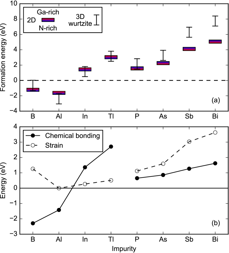
We begin by presenting the results of the band gap changes due to incorporation of individual isoelectronic impurities into the host 2D-GaN structure as shown in Fig. 1a. The group-III elements do not change the band gap significantly with boron reducing the band gap the most in a dilute limit. In contrast, group-V elements affect the band gap much more significantly. Figure 1a includes data for the bulk wurtzite GaN. Notably changes of the band gap due to impurities in the bulk correlate with that in the monolayer.
Results for the bulk GaN can be compared to experimental values of the band gap variation taken linearly up to % concentration at room temperature: 1 meV/% for AlxGa1-xN Brunner et al. (1997); Lee et al. (1999) and meV/% for InxGa1-xN Shan et al. (1996); Matsuoka et al. (2002), which are consistent with our results. Furthermore, previous theoretical calculations of wurtzite GaN1-xPx structures yield a band gap variation of meV/% to 10% of P Bi and Tu (1996), meV/% for 6% of As in GaN1-xAsx Tan and Tansu (2015), and meV/% for 10% of Sb in GaN1-xSbx Sheetz et al. (2011) that show similar trends to our calculations. The theoretical calculations capture experimental trends, however quantitatively the calculated band gap variation may contain errors ranging from meV/% for group-III elements to meV/% for group-V elements. Possible reasons for discrepancy include alloy statistics and clustering effects that are not captured in the calculation of supercells with a single impurity atom.

The band offsets due to impurities in 2D-GaN are shown in Fig. 1b. Remarkably all impurities raise the valence band edge (VBE) more than the conduction band edge (CBE) with exception of boron and aluminum. The group-V elements have a much stronger effect on the VBE when substituted in 2D-GaN as compared to group-III elements. Variations in the Born effective charge of impurities shown in Table 1 aid in explaining this effect. In general, perturbations in the valence band scale with the electropositivity of the substituted element (increase in ). The shift of the valence band edge due to group-V impurities can be viewed as introducing a trap state in the vicinity of the VBE. Similarly, substituting nitrogen into a 2D-GaAs host lattice produces perturbations to the CBE, which correlates with N being more electronegative element than As. This feature is not unique to 2D-GaN and was previously reported for the bulk GaN and GaAs Mattila and Zunger (1998); Bellaiche et al. (1996); O’Reilly et al. (2009); Pashartis and Rubel (2017). Dilute borides seem to provide the only possibility for engineering a conduction band offset as it is the most electronegative element that can be introduced in the host. Note that the estimated inaccuracy in the band offsets is less than 5 meV/% for group-III elements and 20 meV/% for group-V elements, which is due to the subtle changes in the average potential of the supercell introduced by impurities.
| Impurity | ||||
|---|---|---|---|---|
| element | VBE | CBE | ||
| B | 2.67 | 0.45 | 0.0170 | 0.0079 |
| Al | 2.82 | 0.45 | 0.0129 | 0.0079 |
| In | 2.80 | 0.45 | 0.0127 | 0.0078 |
| Tl | 2.82 | 0.45 | 0.0137 | 0.0078 |
| P | 1.93 | 0.29 | 0.2614 | 0.0079 |
| As | 1.74 | 0.28 | 0.4016 | 0.0079 |
| Sb | 1.38 | 0.28 | 0.2849 | 0.0080 |
| Bi | 1.18 | 0.24 | 0.4015 | 0.0080 |
| ref. 2D-GaN | 3.04 | 0.33 | 0.0127 | 0.0078 |
The lack of a direct band gap in the planar 2D-GaN requires changes in the band dispersion in order to facilitate optical transitions. Localized states due to the impurities relax the momentum conservation requirement and thus enable direct optical transitions. An inverse participation ratio (IPR) criterion that quantifies localization across the structure was introduced by Wegner (1980). It can be viewed as a statistical method that determines a normalized variance of the wavefunction constructed from second moments. Here we use a discrete version of IPR Murphy et al. (2011) that is evaluated on the basis of probabilities of finding an electron with an eigenenergy within the muffin tin spheres centred at atomic sites
| (1) |
The summation index runs over all atomic sites. Here the participation ratio represents a number of atomic sites, which confine the wave function with being the upper limit of IPR. The lower limit of IPR, , is the inverse number of atoms in the lattice that corresponds to extended Bloch states.
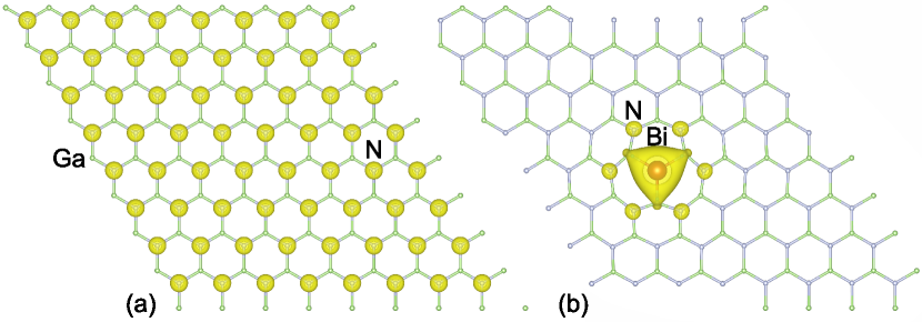
The IPRs in our structures at the band edges can be found in Table 1. The CBE is insignificantly affected by any of the substitutional elements, even when their incorporation is accompanied by a significant lattice strain due to the size mismatch as in the case of Bi and Tl. The VBE demonstrates a minor increase in localization for group-III elements since Ga and the substitutional elements are electronically similar in the presence of N, as evident from the similar values of the Born effective charges (Table 1). The group-V elements introduce strongly localized states in the valence band (an order of magnitude larger IPR), which can be attributed to their much more electropositive nature than N by more than a single elementary charge in . The localization can be visually observed in Fig. 2. The VBE isosurfaces are centered at the N-sites in the host structure but reside almost entirely on the substituted Bi-atom in GaN:Bi. Chemical trends in localization characteristics of III-V impurities in 2D-GaN are very similar to those previously reported by Bellaiche et al. (1996) for the bulk GaN.
The feasibility of incorporating the alloying element into GaN is assessed by calculating defect formation energies due to individual impurity elements following the method outlined in Ref. Freysoldt et al., 2014. The defect formation energy (here demonstrated for a general group-III substitution ) is calculated using the DFT total energy of the supercell with an impurity as well as the respective host structure
| (2) | |||||
The DFT total energies of bulk naturally occurring structures are taken to represent the chemical potential of impurities . The gallium chemical potential is confined within the range
| (3) |
where is the calculated formation enthalpy of GaN ( and eV for the 2D hexagonal planar and bulk wurtzite structures, respectively) determined as
| (4) |
The upper/lower limit of corresponds Ga rich/poor growth conditions.
The results of the defect formation energy calculations are presented in Fig. 3a. Among all III-V elements only B or Al substitutions are energetically favourable. Indium has a limited solubility in the bulk GaN Ho and Stringfellow (1996), and the same is expected for 2D-GaN due to the similar values. The energy penalty associated with the incorporation of a group-V element in 2D-GaN is systematically lower than in the bulk. Due to the relaxed strain conditions in monolayers, 2D materials may generically be more easily alloyed than their bulk counterparts. Phosphorus has a similar defect formation energy to indium in 2D-GaN, which suggest the possibility for practical realization of dilute metastable 2D-GaN1-xPx.
To shed light on the physics behind observed chemical trends in the formation energies of the group III-V substitutions, we decomposed the values into the strain energy and chemical energy components. The strain and chemical energies are defined as
| (5a) | |||||
| (5b) | |||||
It can be shown that correspond to the upper limit of in Eq. (2). The values of and attained are presented in Fig. 3b. In the case of boron the high strain energy is compensated by the strong chemical bonding. The incorporation of In and Tl is primarily limited by the weak chemical bonding. In contrast, the solubility of group-V elements is impeded by a high strain energy due to the large variance in the atomic size from the host N.
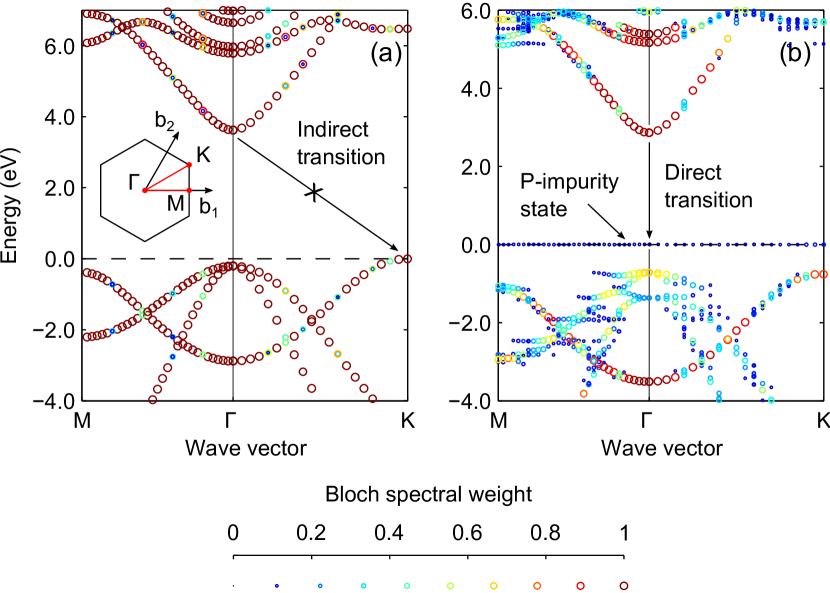
The analysis of the defect formation energies and the band gap reduction efficiency points to a dilute 2D-GaN1-xPx alloy as a favourable candidate for 2D-GaN-based light emitters in the visible spectrum. With this purpose in mind we investigated optoelectronic properties of GaN0.96P0.04 using the Heyd-Scuseria-Ernzerhof (HSE06) screened hybrid functional Heyd et al. (2003); Krukau et al. (2006) intended to overcome the band gap underestimation inherent to DFT semilocal exchange correlation functionals. We have estimated the lattice constant of the GaN1-xPx alloy using Vegard’s law. Reduction of the band gap by 0.57 eV is observed with respect to the host 2D-GaN. The effective band structure unfolded to a primitive Brillouin zone using fold2Bloch package Rubel et al. (2014) is shown in Fig. 4. Phosphorous introduces a dispersionless state approximately 0.6 eV above the host valence band. The lack of a well-defined Bloch character is consistent with the strong localization at the VBE for all group-V impurities (Table 1).
A non-zero dipole transition matrix element is expected due to a direct optical transition between P-state and the conduction band edge, whose Bloch character at -point is well preserved. A similar strategy is employed in green LEDs based on the bulk dilute ( cm-3) nitrogen-dopped GaP Dapkus et al. (1974). Although 2D-GaN0.96P0.04 is an optically active material, the dipole matrix element for a direct transition in Fig. 4b is two orders of magnitude weaker than the matrix element in the planar 2D-GaN. This result can be attributed to a weak -character of the P-related state as evident from the unfolded band structure. Thus, the intrinsically direct band gap of a few-layered 2D-GaN Al Balushi et al. (2016) makes it an attractive alternative to the planar structures for optical emitters. One would expect the behaviour of impurities in a few-layered 2D-GaN to fall between our results for the planar monolayer 2D-GaN and the bulk GaN depending on the layer thickness.
IV Conclusion
Isoelectronic substitutions into a host monolayer 2D-GaN were explored to achieve optical emission with a tuneable wavelength in the visible spectrum. Low-dimensional materials may generally be less strenuous to alloy than bulk materials due to fewer geometrical constraints. Incorporation of phosphorous among other III-V elements enables a much more efficient band gap reduction than indium while featuring similar impurity formation energies. The band gap reduction of the order meV per %P in dilute 2D-GaN1-xPx is mediated by formation of a localized state above the valence band edge of the host 2D-GaN. Concurrently, the conduction band remains resistant to perturbations irrespective of the substitutional element. The phosphorous impurity state facilitates a direct optical transition in otherwise indirect planar monolayer 2D-GaN, which becomes possible due to the electronic localization and the associated relaxation of the wave vector selection rule.
Acknowledgements.
Authors would like to thank Maciej Polak (Wroclaw University of Science and Technology) and Alex Pofelski (McMaster University) for critical reading and valuable discussions. Funding was provided by the Natural Sciences and Engineering Research Council of Canada under the Discovery Grant Program RGPIN-2015-04518. C.P. would like to acknowledge support by the Ontario Graduate Scholarship. This work was performed using computational resources of the Thunder Bay Regional Research Institute, Lakehead University, and Compute Canada (Calcul Quebec).References
- Mas-Balleste et al. (2011) Ruben Mas-Balleste, Cristina Gomez-Navarro, Julio Gomez-Herrero, and Felix Zamora, “2D materials: to graphene and beyond,” Nanoscale 3, 20–30 (2011).
- Fiori et al. (2014) Gianluca Fiori, Francesco Bonaccorso, Giuseppe Iannaccone, Tomás Palacios, Daniel Neumaier, Alan Seabaugh, Sanjay K Banerjee, and Luigi Colombo, “Electronics based on two-dimensional materials,” Nat. Nanotechnol. 9, 768–779 (2014).
- Koppens et al. (2014) F. H. L. Koppens, T. Mueller, Ph. Avouris, A. C. Ferrari, M. S. Vitiello, and M. Polini, “Photodetectors based on graphene, other two-dimensional materials and hybrid systems,” Nat. Nanotechnol. 9, 780–793 (2014).
- Wang et al. (2012) Qing Hua Wang, Kourosh Kalantar-Zadeh, Andras Kis, Jonathan N. Coleman, and Michael S. Strano, “Electronics and optoelectronics of two-dimensional transition metal dichalcogenides,” Nat. Nanotechnol. 7, 699–712 (2012).
- Butler et al. (2013) Sheneve Z. Butler, Shawna M. Hollen, Linyou Cao, Yi Cui, Jay A. Gupta, Humberto R. Gutiérrez, Tony F. Heinz, Seung Sae Hong, Jiaxing Huang, Ariel F. Ismach, Ezekiel Johnston-Halperin, Masaru Kuno, Vladimir V. Plashnitsa, Richard D. Robinson, Rodney S. Ruoff, Sayeef Salahuddin, Jie Shan, Li Shi, Michael G. Spencer, Mauricio Terrones, Wolfgang Windl, and Joshua E. Goldberger, “Progress, challenges, and opportunities in two-dimensional materials beyond graphene,” ACS Nano 7, 2898–2926 (2013).
- Koma (1992) Atsushi Koma, “Van der Waals epitaxy—a new epitaxial growth method for a highly lattice-mismatched system,” Thin Solid Films 216, 72–76 (1992).
- Geim and Grigorieva (2013) A. K. Geim and I. V. Grigorieva, “Van der Waals heterostructures,” Nature 499, 419–425 (2013).
- Blase et al. (1995) X. Blase, Angel Rubio, Steven G. Louie, and Marvin L. Cohen, “Quasiparticle band structure of bulk hexagonal boron nitride and related systems,” Phys. Rev. B 51, 6868–6875 (1995).
- Şahin et al. (2009) Hasan Şahin, Seymur Cahangirov, Mehmet Topsakal, E Bekaroglu, E Akturk, Ramazan Tuğrul Senger, and Salim Ciraci, “Monolayer honeycomb structures of group-IV elements and III-V binary compounds: First-principles calculations,” Phys. Rev. B 80, 155453 (2009).
- Zhuang et al. (2013) Houlong L. Zhuang, Arunima K. Singh, and Richard G. Hennig, “Computational discovery of single-layer III-V materials,” Phys. Rev. B 87, 165415 (2013).
- Al Balushi et al. (2016) Zakaria Y. Al Balushi, Ke Wang, Ram Krishna Ghosh, Rafael A. Vilá, Sarah M. Eichfeld, Joshua D. Caldwell, Xiaoye Qin, Yu-Chuan Lin, Paul A. DeSario, Greg Stone, Shruti Subramanian, Dennis F. Paul, Robert M. Wallace, Suman Datta, Joan M. Redwing, and Joshua A. Robinson, “Two-dimensional gallium nitride realized via graphene encapsulation,” Nat. Mater. 15, 1166–1171 (2016).
- Jiang et al. (2017) Zeyu Jiang, Zhirong Liu, Yuanchang Li, and Wenhui Duan, “Scaling universality between band gap and exciton binding energy of two-dimensional semiconductors,” Phys. Rev. Lett. 118, 266401 (2017).
- Ramasubramaniam et al. (2011) Ashwin Ramasubramaniam, Doron Naveh, and Elias Towe, “Tunable band gaps in bilayer transition-metal dichalcogenides,” Phys. Rev. B 84, 205325 (2011).
- Hanbicki et al. (2015) A. T. Hanbicki, M. Currie, G. Kioseoglou, A. L. Friedman, and B. T. Jonker, “Measurement of high exciton binding energy in the monolayer transition-metal dichalcogenides WS2 and WSe2,” Solid State Commun. 203, 16–20 (2015).
- Kohn and Sham (1965) W. Kohn and L. J. Sham, “Self-consistent equations including exchange and correlation effects,” Phys. Rev. 140, A1133–A1138 (1965).
- Kresse and Furthmüller (1996a) Georg Kresse and Jürgen Furthmüller, “Efficient iterative schemes for ab initio total-energy calculations using a plane-wave basis set,” Phys. Rev. B 54, 11169 (1996a).
- Kresse and Furthmüller (1996b) Georg Kresse and Jürgen Furthmüller, “Efficiency of ab-initio total energy calculations for metals and semiconductors using a plane-wave basis set,” Comp. Mater. Sci. 6, 15–50 (1996b).
- Perdew et al. (2008) John P. Perdew, Adrienn Ruzsinszky, Gábor I. Csonka, Oleg A. Vydrov, Gustavo E. Scuseria, Lucian A. Constantin, Xiaolan Zhou, and Kieron Burke, “Restoring the density-gradient expansion for exchange in solids and surfaces,” Phys. Rev. Lett. 100, 136406 (2008).
- Ranade et al. (2000) M. R. Ranade, F. Tessier, A. Navrotsky, V. J. Leppert, S. H. Risbud, F. J. DiSalvo, and C. M. Balkas, “Enthalpy of formation of gallium nitride,” J. Phys. Chem. B 104, 4060–4063 (2000).
- Jacob and Rajitha (2009) K. T. Jacob and G. Rajitha, “Discussion of enthalpy, entropy and free energy of formation of GaN,” J. Cryst. Growth 311, 3806–3810 (2009).
- Blöchl (1994) Peter E Blöchl, “Projector augmented-wave method,” Phys. Rev. B 50, 17953 (1994).
- Gajdoš et al. (2006) M. Gajdoš, K. Hummer, G. Kresse, J. Furthmüller, and F. Bechstedt, “Linear optical properties in the projector-augmented wave methodology,” Phys. Rev. B 73, 045112 (2006).
- Brunner et al. (1997) D. Brunner, H. Angerer, E. Bustarret, F. Freudenberg, R. Höpler, R. Dimitrov, O. Ambacher, and M. Stutzmann, “Optical constants of epitaxial AlGaN films and their temperature dependence,” J. Appl. Phys. 82, 5090–5096 (1997).
- Lee et al. (1999) S. R. Lee, A. F. Wright, M. H. Crawford, G. A. Petersen, J. Han, and R. M. Biefeld, “The band-gap bowing of AlxGa1-xN alloys,” Appl. Phys. Lett. 74, 3344–3346 (1999).
- Shan et al. (1996) W. Shan, B. D. Little, J. J. Song, Z. C. Feng, M. Schurman, and R. A. Stall, “Optical transitions in InxGa1-xN alloys grown by metalorganic chemical vapor deposition,” Appl. Phys. Lett. 69, 3315–3317 (1996).
- Matsuoka et al. (2002) Takashi Matsuoka, Hiroshi Okamoto, Masashi Nakao, Hiroshi Harima, and Eiji Kurimoto, “Optical bandgap energy of wurtzite InN,” Appl. Phys. Lett. 81, 1246–1248 (2002).
- Bi and Tu (1996) W. G. Bi and C. W. Tu, “N incorporation in GaP and band gap bowing of GaNxP1-x,” Appl. Phys. Lett. 69, 3710–3712 (1996).
- Tan and Tansu (2015) Chee-Keong Tan and Nelson Tansu, “First-principle natural band alignment of GaN/dilute-As GaNAs alloy,” AIP Adv. 5, 017129 (2015).
- Sheetz et al. (2011) R Michael Sheetz, Ernst Richter, Antonis N Andriotis, Sergey Lisenkov, Chandrashekhar Pendyala, Mahendra K Sunkara, and Madhu Menon, “Visible-light absorption and large band-gap bowing of GaN1-x Sbx from first principles,” Phys. Rev. B 84, 075304 (2011).
- Mattila and Zunger (1998) T. Mattila and Alex Zunger, “Deep electronic gap levels induced by isovalent P and As impurities in GaN,” Phys. Rev. B 58, 1367–1373 (1998).
- Bellaiche et al. (1996) L. Bellaiche, S. H. Wei, and Alex Zunger, “Localization and percolation in semiconductor alloys: GaAsN vs GaAsP,” Phys. Rev. B 54, 17568–17576 (1996).
- O’Reilly et al. (2009) E. P. O’Reilly, A. Lindsay, P. J. Klar, A. Polimeni, and M. Capizzi, “Trends in the electronic structure of dilute nitride alloys,” Semicond. Sci. Tech. 24, 033001 (2009).
- Pashartis and Rubel (2017) C. Pashartis and O. Rubel, “Localization of electronic states in III-V semiconductor alloys: a comparative study,” Phys. Rev. Appl. 7, 064011 (2017).
- Wegner (1980) Franz Wegner, “Inverse participation ratio in dimensions,” Z. Phys. B: Condens. Matter 36, 209–214 (1980).
- Murphy et al. (2011) N. C. Murphy, R. Wortis, and W. A. Atkinson, “Generalized inverse participation ratio as a possible measure of localization for interacting systems,” Phys. Rev. B 83, 184206 (2011).
- Momma and Izumi (2011) Koichi Momma and Fujio Izumi, “VESTA 3 for three-dimensional visualization of crystal, volumetric and morphology data,” J. Appl. Crystallogr. 44, 1272–1276 (2011).
- Freysoldt et al. (2014) Christoph Freysoldt, Blazej Grabowski, Tilmann Hickel, Jörg Neugebauer, Georg Kresse, Anderson Janotti, and Chris G. Van de Walle, “First-principles calculations for point defects in solids,” Rev. Mod. Phys. 86, 253–305 (2014).
- Ho and Stringfellow (1996) I. Ho and G. B. Stringfellow, “Solid phase immiscibility in GaInN,” Appl. Phys. Lett. 69, 2701–2703 (1996).
- Heyd et al. (2003) Jochen Heyd, Gustavo E. Scuseria, and Matthias Ernzerhof, “Hybrid functionals based on a screened Coulomb potential,” J. Chem. Phys. 118, 8207 (2003).
- Krukau et al. (2006) Aliaksandr V. Krukau, Oleg A. Vydrov, Artur F. Izmaylov, and Gustavo E. Scuseria, “Influence of the exchange screening parameter on the performance of screened hybrid functionals,” J. Chem. Phys. 125, 224106 (2006).
- Rubel et al. (2014) O. Rubel, A. Bokhanchuk, S. J. Ahmed, and E. Assmann, “Unfolding the band structure of disordered solids: from bound states to high-mobility Kane fermions,” Phys. Rev. B 90, 115202 (2014).
- Dapkus et al. (1974) P. D. Dapkus, W. H. Hackett Jr., O. G. Lorimor, and R. Z. Bachrach, “Kinetics of recombination in nitrogen-doped GaP,” J. Appl. Phys. 45, 4920–4930 (1974).