Electron and thermal transport via Variable Range Hopping in MoSe2 single crystals
Abstract
Bulk single crystal Molybdenum diselenide has been studied for its electronic and thermal transport properties. We perform resistivity measurements with current in-plane (CIP) and current perpendicular to plane (CPP) as a function of temperature. The CIP measurements exhibit metal to semiconductor transition at K. In the semiconducting phase ( K), the transport is best explained by variable range hopping (VRH) model. Large magnitude of resistivity in CPP mode indicates strong structural anisotropy. Seebeck coefficient as a function of temperature measured in the range K, also agrees well with the VRH model. The room temperature Seebeck coefficient is found to be V/K. VRH fittings of the resistivity and Seebeck coefficient data indicate high degree of localization.
I Introduction
Transition metal dichalcogenides (TMDCs) have significantly contributed to the recent advances in two dimensional materials. They are layered materials composed of transition metal (M) and chalcogens (X) in the form MX2. TMDCs provide a wide platform to explore highly interesting quantum phases of matter like charge density waves, superconducting phase transition, metal to insulator transitions and so on. They possess advantageous properties for nanodevice applications like large Seebeck coefficient, non-saturating magnetoresistance, superconductivity, tunable band-gap etc. Wang et al. (2012); Ali et al. (2014); Splendiani et al. (2010); Qi et al. (2016); Mak et al. (2010); Radisavljevic et al. (2010); Ovchinnikov et al. (2014); Qiu et al. (2015). This makes TMDCs highly pertinent for research both fundamentally and technologically. In this work, we explore Molybdenum Diselenide (MoSe2) in its intrinsic semiconducting phase. MoSe2 has found wide variety of applications in optoelectronic and photovoltaic nanodevices Tongay et al. (2012); Wang et al. (2012). Field effect transistors of MoSe2 display a large on-off ratio () and significant mobility ( cm2 V-1 s-1)Larentis, Fallahazad, and Tutuc (2012); Chamlagain et al. (2014); Pradhan et al. (2014). MoSe2 has also been reported to have a negative magnetoresistance Dau et al. (2017). It exhibits exotic phenomena that are rich in fundamental physics (Kumar and Schwingenschlo, 2015; Zhao et al., 2015; Tongay et al., 2012; Bernede, Pouzet, and Alaoui, 1990; Wieting, Grisel, and Levy, 1980). We conduct a study on bulk MoSe2 single crystals and present intriguing features which are of high scientific interest.
We study electron and thermal transport properties of MoSe2 through resistivity and Seebeck coefficient measurements. Resistivity measurements as a function of temperature reveal scattering mechanism involved at various temperature regime. We infer that the appropriate transport mechanism that best explains the data is variable range hopping (VRH) mechanism proposed by Mott in 1969 Mott (1969); Mott and Davis (1979); Mott (1990, 1978). According to this model, conduction of charge carriers occurs via hopping mechanism. The electrons hop between localized states in the crystal Ambegaokar, Halperin, and Langer (1971), for which the necessary energy is provided by phonons. The resistivity is given by,
| (1) |
where is the dimensionality. In this model density of states close to the fermi level is assumed to be constant. Using the VRH model, Seebeck coefficient calculations by Chaikin et.al. Burns and Chaikin (1985) lead to a temperature dependence of Seebeck coefficient given by,
| (2) |
where, is the density of states, is the density of states when interaction is turned off, is the decay length of the wave function considered and is the dimension. Hence the overall dependence of on will be given by,
| (3) |
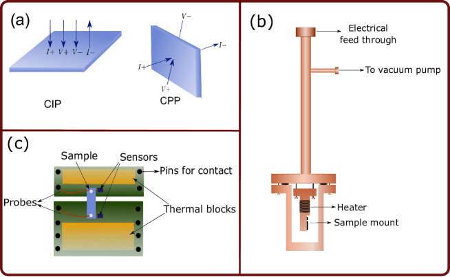
We present a detailed experimental study of resistivity measurements for current in-plane (CIP) mode and current perpendicular to plane (CPP) mode, the schematics of which are shown in Fig. 1(a). Resistivity in CIP mode shows a very intriguing feature of metal to semiconductor transition at low temperature. At higher temperatures the transport exhibits semiconducting phase and the mechanism is primarily through hopping between localized states. Measurements in CPP mode also show semiconducting phase with conduction via hopping. We perform in-plane Seebeck coefficient measurements (Fig. 1(b)) for which the data fits best for the VRH model.
It has been reported that two dimensional nature of the material, supports larger Seebeck coefficient Imai, Shimakawa, and Kubo (2001). Large magnitude of Seebeck coefficient encourages us to look for properties which might support Phonon Glass Electron Crystal (PGEC) behavior in this material Takabatake et al. (2014); Beekman, Morelli, and Nolas (2015); Wu et al. (2014); Snyder and Toberer (2008). This concept aims to engineer materials with low thermal conductivity (high phonon-phonon scattering as in glass) and high electronic conductivity (perfect crystal like behavior for electrons). TMDCs might satisfy this requirement due to their anisotropic crystal structure Beekman, Morelli, and Nolas (2015). In further sections we present the experimental details and the results of the study, and lastly conclusions.
II Experimental details
We perform DC resistivity measurements in CIP and CPP modes using standard four probe technique. Typical sample dimensions are: thickness mm and area mm mm. The sample is mounted on the chip customized for measurements in closed cycle He cryostat (Oxford Cryomech PT405). Oxford MercuryiTC temperature controller is used along with the cryostat, for temperature dependent measurements between 9-300 K. Keithely 2401 sourcemeter and Keithley 2182A nanovoltmeter are used to source current and measure voltage respectively. Contacts are made using silver paste on the same side of the sample for CIP measurements and on opposite sides for CPP measurements as shown in fig. 1 (a).
The Seebeck measurements are performed in an in-house built dip-stick which is calibrated using measurements on standard samples. As shown in fig. 2 (b) resistivity dip stick consists of a long stainless steel tube whose one end consists of the sample mounting pins. Wires drawn out from these pins are connected to external hardware by means of electrical feed through at the other end. The tube has an extension to vacuum pump. The sample end is sealed in a copper can and maintained in a vacuum of the order of 10-3 mbar for temperature dependent measurements. The sample mount is shown in detail in fig. 2 (c). The sample is placed between two thermal blocks separated by an air gap of mm (Fig. 1 (c)). Copper wires are used as probes to measure thermal voltage. Contacts are made on the sample using silver paste. Miniature temperature sensors (Pt-100) are placed in close proximity to the probes to record the temperature. The sample is electrically insulated from the thermal block through a mica sheet. The entire unit is mounted at one end of the dip stick. The dip stick is dipped in a liquid nitrogen dewar for temperature dependent measurements. Temperature at the two ends of the sample and the thermal voltage are measured using the Lakeshore 336 temperature controller and Keithley 2182A nanovoltmeter respectively. The entire system is LabVIEW automated.
III Results and Discussions
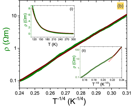
Figure 2 (a) shows resistivity as a function of temperature in the range K in CIP mode in high vacuum of mbar. Resistivity increases linearly in the range K, like in metals Kittle (1996) (Inset (i) Fig. 2 (a)). We observe a metal to semiconductor transition (Inset (ii) Fig. 2(a)) at K. The resistivity behavior in the semiconducting phase can be explained by VRH model, according to which hopping between localized states is mediated by phonons. Above K resistivity falls with temperature as given by Eq. (1), where , and are fitting parameters (Inset (ii) Fig. 2(a) shows raw data with VRH fitting of Eq. (1)). To show the quality of the fit, we also show resistivity (in log scale) as a function of in Fig. 2 (a). The value for obtained from this fit is K. This large value of is attributed to high degree of localization due to disorders. This value is comparable to the value reported in few layer MoSe2 Roy et al. (2016); Mos et al. (2011). This suggests that the localization length is small and the hence we observe VRH mechanism till room temperature in our experiment Roy et al. (2016); Arya, Prasad, and Anil Kumar (2012); Shiraishi, Ramm, and Ata (2002).
We analyse the data for other possible transport mechanisms, details of which are discussed in supplementary information. An Arrhenius fit to the data gave impractically small magnitude of activation energy, . This suggests that the transport mechanism is different from thermionic excitations.
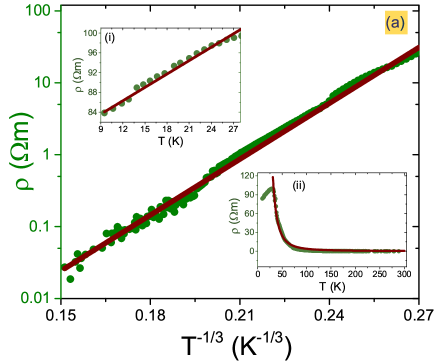
MoSe2 has strong structural anisotropy (shown in further results for CPP measurements) and high degree of localization. As seen in fig. 2 (a), with decrease in temperature, divergence in resistivity is expected. However, we observe a down turn in resistivity, which varies linearly with temperature. This semiconductor to metal phase transition at K observed in our experiment is highly intriguing which maybe attributed to disorder controlled divergence in resistivity as discussed by earlier works on phase transitions in disordered systems Lee et al. (2013); Dubi, Meir, and Avishai (2007); Crane et al. (2007); Ying et al. (2016); Fujita, Uchida, and Eisaki (2006). In two dimensional quasi-1D systems of the MoSe2 family, superconducting phase transition has been observed at lower temperatures Petrović et al. (2016); Das Sarma and Hwang (2014); Singh et al. (2012); Bergk et al. (2011); Arutyunov, Golubev, and Zaikin (2008). Petrovic et.al. Petrović et al. (2016) show that for Na2-δMo6Se6, resistivity as K, increases monotonically with degree of disorder. In our case disorder parameter is of the order of , which corresponds to a finite at low temperature. Resistivity measurements at lower temperatures will reveal the emergent electronic phases of MoSe2, whether it continues in metal like phase or undergo a superconducting phase transition assisted by Quantum phase slip. However the operational range of our experimental set-up limits the measurements to K. It must be noted that the value of resistivity observed is too large compared with that of normal metals ( m). This linear behavior maybe attributed to disorders, anisotropy and interactions between electrons Rowe (1995) unlike electron-phonon scattering in normal metals.
Figure 2 (b) shows Seebeck coefficient versus temperature data in the range K. Temperature dependence of Seebeck coefficient is given by Eq. (3), where in our case. Seebeck coefficient in the VRH model has been explained in two ways. First, by the Mott picture where varies as stated above. In this case the interaction is not considered and resistivity is given by, Eq. (1). Second, the Efros picture considers interaction and predicts that below certain critical temperature the conductivity is given by Burns and Chaikin (1985). This model predicts that the Seebeck coefficient is constant over the temperature range in which interactions are predominant. Figure 2 (b) shows Seebeck coefficient increase with temperature in accordance with Motts picture (). Clearly we do not observe constant Seebeck coefficient nor the resistivity as per Efros’ picture. The resistivity and the Seebeck both follow Motts model for electron and thermal transport. Hence we infer the dominant interaction in this temperature regime ( K) is electron-phonon interaction as explained by the Mott VRH model.
We find that the Seebeck coefficient increases as upto K. Beyond 225 K, the fit deviates due to effects of thermally generated charge carriers Bentley (1998). In the whole temperature range the sign of Seebeck coefficient was negative. We find the Seebeck coefficient to be V/K near to room temperature for bulk samples. This is significantly a large number for bulk sample in par with the ones which have been hitherto reported Liu et al. (2013); Imai, Shimakawa, and Kubo (2001). Monolayer or few layer devices of MoSe2 might have a much larger Seebeck coefficient than the bulk Lee et al. (2016); Delatorre et al. (2003).
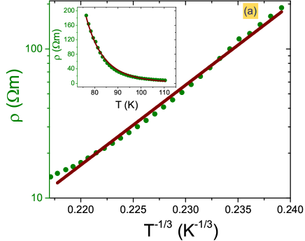
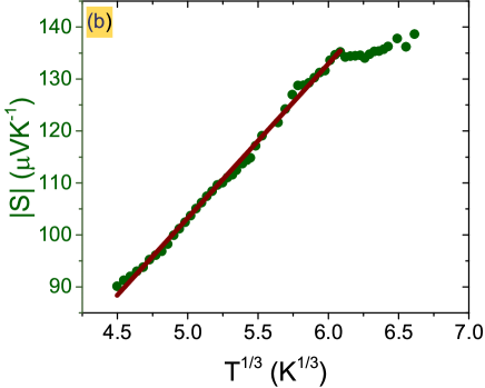
Results of resistivity measurement for CPP mode in the range K are shown in Fig. 3. For temperatures below K, electrons freezing limits the operational range of the setup. Due to strong structural anisotropy, magnitude of resistivity in CPP mode is at least three orders larger than that in CIP mode. The temperature dependence of resistivity in CPP configuration varies from that in CIP mode. Figure 3 (a) shows resistivity data as a function of in the range K (Inset (i) shows ). The VRH model fitting as in Eq. (1) for CPP mode gives a good fit for in this range; is of the order of K. Hence we conclude that in this temperature range, transport is dominated by intralayer hopping. Figure 3 (b) shows resistivity as a function of in the range K in log scale (Inset shows ). This corresponds to resistivity with in the Mott VRH model ; is of the order of K. The crossover from to is explicitly shown in inset (ii) of Fig. 3 (b). We infer that the transport via hopping mechanism follows D bulk like behavior at higher temperatures. In this temperature range interlayer hopping also contributes to the transport. The fitting parameter relates to the degree of disorder in the system. We find large magnitude of in CPP than that in CIP which is as expected.
IV Conclusions
To summarize, we have experimentally investigated the electron and thermal transport in MoSe2 through temperature dependent resistivity and Seebeck measurements. The CIP resistivity shows linear behavior with temperature upto K. For K, we have performed fitting according to the VRH model and observed that the transport in the intrinsic semiconducting phase is governed by localized states. Large magnitude of , in the VRH model fit indicates high degree of localization. Temperature dependent resistivity measurements for K will answer the curiosity on the phases that might occur at low temperatures. Resistivity in CPP mode is much larger ( 3 orders) than the CIP mode, which clearly indicates strong structural anisotropy. The transport occurs in two dimensional regime upto K and exhibits bulk behavior above K. In-plane Seebeck measurements also show VRH transport mechanism. For a bulk material the room temperature Seebeck coefficient is significantly large, and in par with materials like MoS2. Seebeck coefficient is expected to have much larger magnitude for thinner or few layer samples. Hence this material is a highly potential candidate for engineering heterostructure devices based on the PGEC concept.
V Supplementary Material
Supplementary information contains discussion for weak localization and Arrhenius excitation for the experimental data in Fig. 2 (a) and XRD spectrum of MoSe2 crystals.
VI Acknowledgements
DS thanks Department of Science and Technology (DST), Govt. of India for PhD fellowship through DST-INSPIRE scheme (DST/INSPIRE Fellowship/2013/742). RSP thanks DST, Govt. of India for financial support (No. SR/NM/MS-1002/2010) through Nanomission program. We thank Abhiram Soori, Diptiman Sen and Radhika Vathsan for illuminating discussions.
References
- Wang et al. (2012) Q. H. Wang, K. Kalantar-zadeh, A. Kis, J. N. Coleman, and M. S. Strano, Nat. Nanotechnol. 7, 699 (2012).
- Ali et al. (2014) M. N. Ali, J. Xiong, S. F. J. Tao, Q. D. Gibson, L. M. S. T. Liang, N. Haldolaarachchige, M. Hirschberger, N. P. Ong, and R. J. Cava, Nature 514, 205 (2014).
- Splendiani et al. (2010) A. Splendiani, L. Sun, Y. Zhang, T. Li, J. Kim, C.-Y. Chim, G. Galli, and F. Wang, Nano Lett. 10, 1271 (2010).
- Qi et al. (2016) Y. Qi, P. G. Naumov, M. N. Ali, C. R. Rajamathi, W. Schnelle, O. Barkalov, M. Hanfland, S.-C. Wu, C. Shekhar, Y. Sun, V. Sub, M. Schmidt, U. Schwarz, E. Pippel, P. Werner, R. Hillebrand, T. Förster, E. Kampert, S. Parkin, R. J. Cava, C. Felser, B. Yan, and S. A. Medvedev, Nat. Commun. 7, 1 (2016).
- Mak et al. (2010) K. F. Mak, C. Lee, J. Hone, J. Shan, and T. F. Heinz, Phys. Rev. Lett. 105, 1 (2010).
- Radisavljevic et al. (2010) B. Radisavljevic, A. Radenovic, J. Brivio, V. Giacometti, and A. Kis, Nat. Nanotechnol. 6, 147 (2010).
- Ovchinnikov et al. (2014) D. Ovchinnikov, A. Allain, Y. S. Huang, D. Dumcenco, and A. Kis, ACS Nano 8, 8174 (2014).
- Qiu et al. (2015) D. Qiu, D. U. Lee, C. S. Park, K. S. Lee, and E. K. Kim, Nanoscale 7, 17556 (2015).
- Tongay et al. (2012) S. Tongay, J. Zhou, C. Ataca, K. Lo, T. S. Matthews, J. Li, C. Grossman, and J. Wu, Nano Lett. , 5576 (2012).
- Larentis, Fallahazad, and Tutuc (2012) S. Larentis, B. Fallahazad, and E. Tutuc, Appl. Phys. Lett. 101 (2012).
- Chamlagain et al. (2014) B. Chamlagain, Q. Li, N. J. Ghimire, H. J. Chuang, M. M. Perera, H. Tu, Y. Xu, M. Pan, D. Xaio, J. Yan, D. Mandrus, and Z. Zhou, ACS Nano 8, 5079 (2014).
- Pradhan et al. (2014) N. R. Pradhan, D. Rhodes, Y. Xin, S. Memaran, L. Bhaskaran, M. Siddiq, S. Hill, P. M. Ajayan, and L. Balicas, ACS Nano 8, 7923 (2014).
- Dau et al. (2017) M. T. Dau, C. Vergnaud, A. Marty, F. Rortais, C. Beigné, H. Boukari, E. Bellet-Amalric, V. Guigoz, O. Renault, C. Alvarez, H. Okuno, P. Pochet, and M. Jamet, Appl. Phys. Lett. 110, 011909 (2017).
- Kumar and Schwingenschlo (2015) S. Kumar and U. Schwingenschlo, Chem. Mater. 27, 1278 (2015).
- Zhao et al. (2015) Z. Zhao, H. Zhang, H. Yuan, S. Wang, Y. Lin, Q. Zeng, G. Xu, Z. Liu, G. K. Solanki, K. D. Patel, Y. Cui, H. Y. Hwang, and W. L. Mao, Nat. Commun. 6, 1 (2015).
- Bernede, Pouzet, and Alaoui (1990) J. C. Bernede, J. Pouzet, and Z. K. Alaoui, Appl. Phys. A 159, 155 (1990).
- Wieting, Grisel, and Levy (1980) T. J. Wieting, A. Grisel, and F. Levy, Physica B+C 99, 337 (1980).
- Mott (1969) N. F. Mott, Philos. Mag. 19, 835 (1969).
- Mott and Davis (1979) N. F. Mott and E. A. Davis, in Electronic processes in non-crystalline materials (Clarendon Press, Oxford, 1979).
- Mott (1990) N. F. Mott, in Metal-Insulator Transitions (Taylor Francis, London, 1990).
- Mott (1978) N. Mott, Rev. Mod. Phys. 50 (1978).
- Ambegaokar, Halperin, and Langer (1971) V. Ambegaokar, B. I. Halperin, and J. S. Langer, Phys. Rev. B 4, 2612 (1971).
- Burns and Chaikin (1985) M. J. Burns and P. M. Chaikin, J. Phys. C: Solid State Phys. 18, L743 (1985).
- Imai, Shimakawa, and Kubo (2001) H. Imai, Y. Shimakawa, and Y. Kubo, Phys. Rev. B 64, 241104 (2001).
- Takabatake et al. (2014) T. Takabatake, K. Suekuni, T. Nakayama, and E. Kaneshita, Rev. Mod. Phys. 86, 669 (2014).
- Beekman, Morelli, and Nolas (2015) M. Beekman, D. T. Morelli, and G. S. Nolas, Nat. Mater. 14, 1182 (2015).
- Wu et al. (2014) J. Wu, H. Schmidt, K. K. Amara, X. Xu, G. Eda, and B. Ozyilmaz, Nano Lett. 14, 2730 (2014).
- Snyder and Toberer (2008) G. J. Snyder and E. S. Toberer, Nat. Mater. 7, 105 (2008).
- Kittle (1996) C. Kittle, in Introduction to Solid State Physics (John Wiley and Sons, Inc., 1996).
- Roy et al. (2016) A. Roy, H. C. P. Movva, B. Satpati, K. Kim, R. Dey, A. Rai, T. Pramanik, S. Guchhait, E. Tutuc, and S. K. Banerjee, Appl. Mater. Interfaces 8, 7396 (2016).
- Mos et al. (2011) T. Mos, S. Ghatak, A. N. Pal, and A. Ghosh, ACS nano 5, 7707 (2011).
- Arya, Prasad, and Anil Kumar (2012) V. P. Arya, V. Prasad, and P. S. Anil Kumar, J. Phys.: Condens. Matter. 24, 245602 (2012).
- Shiraishi, Ramm, and Ata (2002) M. Shiraishi, M. Ramm, and M. Ata, Appl. Phys. A 74, 613 (2002).
- Lee et al. (2013) Y. Lee, A. Frydman, T. Chen, B. Skinner, and A. M. Goldman, Phys. Rev. B 88, 024509 (2013).
- Dubi, Meir, and Avishai (2007) Y. Dubi, Y. Meir, and Y. Avishai, Nature 449, 876 (2007).
- Crane et al. (2007) R. Crane, N. P. Armitage, A. Johansson, G. Sambandamurthy, D. Shahar, and G. Grüner, Phys. Rev. B 75, 184530 (2007).
- Ying et al. (2016) T. Ying, Y. Gu, X. Chen, X. Wang, S. Jin, L. Zhao, W. Zhang, and X. Chen, Sci. Adv. 2, e1501283 (2016).
- Fujita, Uchida, and Eisaki (2006) K. Fujita, S.-i. Uchida, and H. Eisaki, AIP Conf. Proc. 850, 977 (2006).
- Petrović et al. (2016) A. P. Petrović, D. Ansermet, D. Chernyshov, M. Hoesch, D. Salloum, P. Gougeon, M. Potel, L. Boeri, and C. Panagopoulos, Nat. Commun. 7, 12262 (2016).
- Das Sarma and Hwang (2014) S. Das Sarma and E. H. Hwang, Phys. Rev. B 89, 1 (2014).
- Singh et al. (2012) F. Singh, B. Chaudhary, V. Kumar, R. G. Singh, S. Kumar, and A. Kapoor, J. Appl. Phys. 112, 073101 (2012).
- Bergk et al. (2011) B. Bergk, A. P. Petrovic, Z. Wang, Y. Wang, D. Salloum, P. Gougeon, M. Potel, and R. Lortz, New Jour. Phys. 13 (2011).
- Arutyunov, Golubev, and Zaikin (2008) K. Y. Arutyunov, D. S. Golubev, and A. D. Zaikin, Phys. Rep. 464, 1 (2008).
- Rowe (1995) D. M. Rowe, in CRC Handbook of Thermoelectrics (CRC Press, 1995) pp. 354–356.
- Bentley (1998) R. E. Bentley, in Handbook of Temperature Measurement Vol. 3: Theory and Practice of Thermoelectric Thermometry (Springer, 1998) p. 72.
- Liu et al. (2013) Y. Liu, P. Sahoo, J. P. A. Makongo, X. Zhou, S.-J. Kim, H. Chi, C. Uher, X. Pan, and P. F. P. Poudeu, J. Am. Chem. Soc 135, 7486 (2013).
- Lee et al. (2016) M.-J. Lee, J.-H. Ahn, J. H. Sung, H. Heo, S. G. Jeon, W. Lee, J. Y. Song, K.-H. Hong, B. Choi, S.-H. Lee, and M.-H. Jo, Nat. Commun. 7, 12011 (2016).
- Delatorre et al. (2003) R. G. Delatorre, M. L. Sartorelli, A. Q. Schervenski, A. A. Pasa, and S. Gths, J. Appl. Phys. 93, 6154 (2003).