Universality of scanning tunneling microscopy in cuprate superconductors
Abstract
We consider the problem of local tunneling into cuprate superconductors, combining model based calculations for the superconducting order parameter with wavefunction information obtained from first principles electronic structure. For some time it has been proposed that scanning tunneling microscopy (STM) spectra do not reflect the properties of the superconducting layer in the CuO2 plane directly beneath the STM tip, but rather a weighted sum of spatially proximate states determined by the details of the tunneling process. These “filter” ideas have been countered with the argument that similar conductance patterns have been seen around impurities and charge ordered states in systems with atomically quite different barrier layers. Here we use a recently developed Wannier function based method to calculate topographies, spectra, conductance maps and normalized conductance maps close to impurities. We find that it is the local planar Cu Wannier function, qualitatively similar for many systems, that controls the form of the tunneling spectrum and the spatial patterns near perturbations. We explain how, despite the fact that STM observables depend on the materials-specific details of the tunneling process and setup parameters, there is an overall universality in the qualitative features of conductance spectra. In particular, we discuss why STM results on Bi2Sr2CaCu2O8 (BSCCO) and Ca2-xNaxCuO2Cl2(NaCCOC) are essentially identical.
pacs:
74.20.-z, 74.70.Xa, 74.62.En, 74.81.-gI Introduction
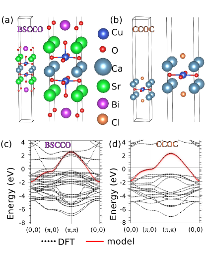
Scanning tunneling microscopy (STM) and spectroscopy (STS) have played an important role in the evolution of ideas about cuprate superconductors, including the -wave symmetry of the superconductivity, the nature of the pseudogap, and the existence of competing ordersFischer et al. (2007); Fujita et al. (2012). On the other hand, exactly what is measured by STM/S has never been completely clear, due to the fact that the superconducting wavefunction is believed to reside primarily in the CuO2 layer, while the STM tip detects a tunneling current ascribed to the density of electronic states several Å above the cleaved surface. Between the two lie insulating barrier layers that are different for each cuprate material. For example, in the canonical STM material Bi2Sr2CaCu2O8 (BSCCO), the insulating layer consists of BiO and SrO planes, with the latter containing a so-called “apical” O atom placed directly above a Cu in the CuO2 plane below the BiO layer at which the system cleaves. In another intensively studied material, Ca2-xNaxCuO2Cl2(NaCCOC), the barrier layer contains planes of Cl and planes of Ca/Na atoms, with no apical O, see Fig. 1 (a)-(b). Instead, NaCCOC contains apical Cl, which reside on the surface of the cleaved layer. If the tunneling process depends on the details of the barrier layer, one might expect to see very different results for different cuprate materials, even if their superconducting states are quite similar. In practice, most theoretical work has ignored this complication and assumed a featureless barrier.
To reveal the effects of the barrier layer most clearly, a homogeneous situation is not ideal, since the range of the tunneling process is hidden by the crystal periodicityNieminen et al. (2009). On the other hand, studies of impurity effects in superconductors have been shown to be very useful in elucidating aspects of the superconductivity Balatsky et al. (2006); Alloul et al. (2009). In cuprates, Zn and Ni impurities have been widely studied as they substitute an in-plane Cu atom and hence directly couple to the electronic states that give rise to the superconducting properties. With a closed d-shell, Zn acts as a strong non-magnetic potential scatterer, whereas, Ni acts as a magnetic scatterer owing to its configuration. The STM tunneling conductance around Zn in BSCCO features a sharp in-gap virtual bound state and drastic suppression of the coherence peaksPan et al. (2000), consistent with the simplest theoretical predictions for a nonmagnetic -function potential Balatsky et al. (1995) in a -wave superconductor. However, the spatial pattern around the impurity site deviates from the predictions of this simple modelBalatsky et al. (2006). Most notably, experiment observes intensity maxima at the impurity sites in contrast to the minima predicted by the theory.
To reconcile theory and experiment, several authors focused on the details of the tunneling process, and advanced a hypothesis that we will refer to as a “filter”; in essence, these works proposed phenomenologically that the tip detected the signal arising from the four nearest neighbor Cu sites, rather than from that immediately below the tipMartin et al. (2002); Zhu et al. (2000). The authors of Ref. Martin et al., 2002 suggested, in particular, that the overlap of the apical oxygen 2 and 3s orbitals with Bi was crucial for the tunneling. While a first principles calculation of a Zn impurity in BSCCO detected a weak filter effectWang et al. (2005), the effect of superconductivity was unknown. More recently, a hybrid theory was proposedChoubey et al. (2014); Kreisel et al. (2015) that accounted for material-specific details by downfolding density functional theory calculations onto a tight-binding model using Cu 3 Wannier functions, and combined this with a phenomenological Bogoliubov-de Gennes (BdG) calculation of -wave superconductivity in this basis. This “BdG+W” theory was able to account for the details of the Zn resonance in BSCCO and many aspects of the quasiparticle interference data on this materialKreisel et al. (2015). Furthermore, using a variant of the same method applicable to type models, it was recently shown Choubey et al. (2017) that the characteristics of -form factor charge order, where charge modulations occur mainly at O sites and are opposite in phase for two inequivalent O atoms Fujita et al. (2014); Comin and Damascelli (2016); Hamidian et al. (2016), can be easily obtained within a one-band calculation by accounting for the O degrees of freedom through the Wannier function.
Nevertheless, while this model successfully accounted for STM data on Zn impurities in BSCCO as well as quasiparticle interference results in exquisite detail, it confirmed that the wavefunctions at the surface detected by the tip were influenced strongly by their hybridization with the apical oxygen 2 states. As discussed above, these apical O states are present in most cuprates, but not in NaCCOC. The previous Wannier-based work thus fails to address the question of the apparent universality of STM observables, e.g. impurity states and charge order, in different cuprate materialsKohsaka et al. (2007). In this paper, we attempt to reconcile the filter proposals with the universality of STM response observed in cuprates.
For this purpose, we apply the BdG+W approach to the impurity problem in both BSCCO and NaCCOC. We review the BSCCO Zn results, and move on to discuss the Ni impurity results from BSCCO, which were not addressed in Ref. Kreisel et al., 2015. STM studies on BSCCO Hudson et al. (2001) have shown two spin-resolved in-gap virtual bound states at energies . Bound state peaks were observed to be particle-like at the impurity site and next nearest neighbor sites, and hole like at the nearest neighbor sites. The spatial patterns at resembled cross-shaped and X shaped at . Observation of these resonance states is consistent with the models of combined potential and magnetic scattering of quasiparticles in -wave superconductorsSalkola et al. (1997). However, as in the case of Zn, spatial patterns deviate from the predictionsSalkola et al. (1997). In one attempt to reconcile theory and experiment “filter” was proposedMartin et al. (2002). Here, we show that the experimental features are easily obtained in the BdG+W approach and, like the Zn problemKreisel et al. (2015), tunneling via nearest neighbor apical oxygen atoms plays a crucial role in shaping the spatial patterns at resonance energies in the local density of states (LDOS) spectrum near Ni impurities.
For the same problem in NaCCOC, we find that the Wannier functions on the surface that couple to the STM tip and the electronic structure at low energies are very similar to BSCCO despite the fact that the material has a different structure and the tunneling takes place through a rather different surface layer. Consequently, the spectral properties and the spatial pattern observed close to strong potential scatterers and also magnetic scatterers are expected to be very similar to those seen in BSCCO. We discuss the implications for observation of charge order in both materials, and for the use of STM to deduce important aspects of superconductivity in the cuprates.
II Model
The method used in this work was introduced earlierChoubey et al. (2014) and already applied to the case of cuprate superconductors alreadyKreisel et al. (2015) as well as in multiband systemsChoubey et al. (2014); Chi et al. (2016). The starting point is a first principles calculation that yields the electronic structure downfolded to a tight-binding model
| (1) |
where are hopping elements between orbitals and on the lattice sites labeled with and and creates an electron at lattice site with spin . To account for correlations, we introduce an overall band renormalization and work away from half filling using a rigid band shift by choosing the chemical potential accordingly. While this is a standard procedure and also a common starting point for model based calculations, we obtain extra information with the Wannier functions that describe the electrons. The field operators of the electrons are related to the lattice operators via
| (2) |
where the Wannier functions are the matrix elements. For application of this approach to cuprates, we restrict consideration to a single Cu orbital, .
In the following we study STM imaging of magnetic impurity states like Ni in cuprates. A magnetic impurity acts as the source of potential as well as magnetic scattering, and can be simply modeled by the following Hamiltonian
| (3) | ||||
The first term in the above Hamiltonian accounts for the potential scattering at the impurity site and is the impurity potential which can be written as , where represents the Kronecker delta function, for a completely local impurity model. The second term in the above Hamiltonian accounts for the magnetic scattering due to the exchange interaction between the impurity magnetic moment, approximated as a classical spin, and the conduction electrons. denotes the extended exchange coupling which can be expressed as for the special case of completely local exchange interaction. Finally, to account for superconductivity we include a mean-field BCS term
| (4) |
where are the pairing mean fields.
III Theoretical approach
III.1 T-matrix approach
For this purpose, we Fourier transform the superconducting order parameter of the homogeneous system to obtain . In this work, we assume a standard -wave order parameter , and write down the Nambu Hamiltonian
| (5) |
where the Fourier transform of the hopping elements has been introduced. Defining a Green’s function of the non-interacting electronic structure via
| (6) |
we transform to real space
| (7) |
in order to calculate the Green’s function in the presence of the impurity
| (8) |
using the T-matrix
| (9) |
Here is the local Green’s function and the impurity potential, split up in a potential part and a magnetic contribution, is given by . The steps presented up to now, are straightforward and widely used in the literature Balatsky et al. (2006); alternative methods to obtain the lattice Green’s function including the modulation of the order parameter in real space (via self-consistency approaches) will be presented in the next section. For the results presented in Sec. IV, we employ the T-matrix approach only for the computationally expensive calculations of STM topographs and related maps.
III.2 BdG approach
The mean-field solution of our problem including all terms of the Hamiltonian
| (10) |
can be found by solving a self-consistency equation where the superconducting order parameter is related to the pair potential through . To get the -wave gap symmetry we set if sites are nearest neighbors and otherwise. The eigenvalue problem corresponding to Eq. (10) can be expressed in the form of BdG equations which is solved self-consistentlyChoubey et al. (2014) for and by keeping the electron number fixed. Using BdG eigenvalues and eigenvectors and , the lattice Green’s function can be obtained as well.
III.3 Calculation of the tunneling conductance
The differential tunneling conductance as measured in an STM experiment at a given bias voltage can be calculated usingTersoff and Hamann (1985)
| (11) |
where the continuum LDOS is given by
| (12) |
where refers to the particle-hole component of the Nambu Green’s function; for broken symmetry in spin space, one needs to take into account also the component at negative energies
| (13) |
Finally, the continuum Green’s function can be calculated by employing a Wannier basis transformationChoubey et al. (2014),
| (14) |
where relation Eq. (2) has been used. Note that the framework can be applied to single and multiband systems, while in the following, all orbital indices are ignored since a one-band model for cuprates is used.
IV Results
IV.1 Electronic structure
The first step in the Wannier function based analysis of STM observables is to construct the tight-binding description of the normal state of the material under study, using first principles calculations. As input for the density functional theory (DFT) calculations, a cell representing the Bi2Sr2CaCu2O8 surface was constructed as follows. First the bulk Bi4Sr4Ca2Cu4O16 unit cell was considered with the structural parameters from Ref. Hybertsen and Mattheiss, 1988. Then half of the atoms were deleted, resulting in a single Bi2Sr2CaCu2O8 layer unit cell with a vacuum of approximately 20 Å, see Fig. 1 (a). A single Ca2CuO2Cl2 (CCOC) layer unit cell was created in a similar way. First the bulk Ca4CuO4Cl4 unit cell was considered with structural parameters taken from Ref. Argyriou et al., 1995. Then again half of the atoms were deleted which creates a certain amount of vacuum. In addition, some vacuum was added such that the total vacuum is again approximately 20 Å. The DFT calculations and subsequent downfolding to the Wannier basis, were performed using the VASPKresse and Furthmüller (1996) and Wannier90 Mostofi et al. (2014) packages, respectively. After the construction of the tight-binding model, calculations are performed for 15% doping implemented by a rigid band shift, roughly appropriate for optimal doping.
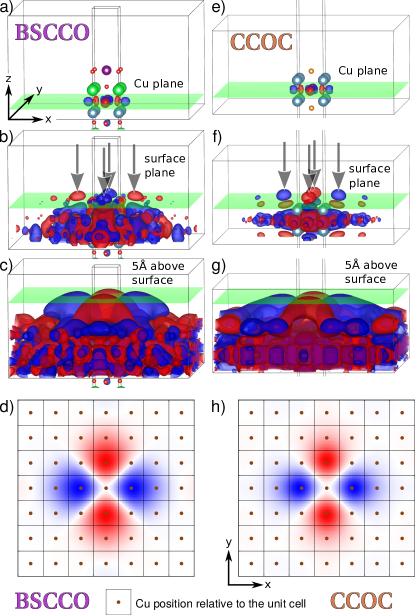
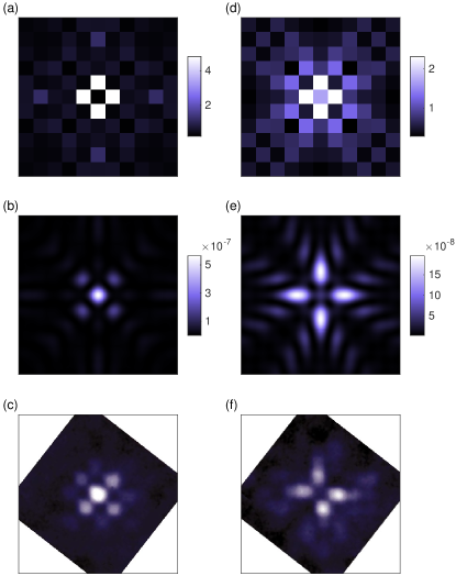
As shown in Fig. 1 (c)-(d), we obtain a very similar tight binding structure for both BSCCO and CCOC, which is generic for many cuprate materials. The Wannier functions generated in this downfolding procedure involve states derived from all atomic species in the unit cell, but restricted to an energy range of a few eV around the Fermi level. The Cu Wannier function important for superconductivity is shown in Fig. 2 to involve not only atomic functions on a given site, but states localized on many nearby atoms. The tunneling process depends on the density of these states, and those associated with Wannier functions on neighboring Cu’s, at a point several Å above the surface. At intermediate isovalues, i.e. distances from a given Cu, the Wannier function is seen in Fig. 2 to be rather complex, and differences between BSCCO and CCOC are evident, reflecting difference in the barrier layer. While in both cases, apical states above the nearest neighbor Cu are clearly visible, in the BSCCO case these are associated with O, while in CCOC they are associated with the Cl. There are also qualitative differences that may be observed upon close inspection of the figure.
However, in the asymptotic regime far from the surface, the Wannier functions for both materials are seen to be almost identical. The symmetry of the Cu wavefunction is the same as dictated by the symmetry of the crystal including the atoms in the layers above the Cu-O layer leading to the vanishing weight directly above the central Cu site; small differences in the extent of the wavefunction, e.g. the positions of the maxima relative to the center, can be observed, see Fig. 2 (d),(h). The maximum in the magnitude of the Wannier function in both compounds occur above the NN Cu sites. It was shown in Ref. Kreisel et al., 2015 that this maximum has the largest contribution from the apical O- states in NN unit cells. In case of CCOC, we find that the NN Cl- states at the surface are responsible for the Wannier function maxima. The similarity of the shape of the surface Wannier function in both compounds leads to the similar spatial structure of impurity states at the STM tip position, as we show in following sections.
IV.2 Effects of a non-magnetic impurity
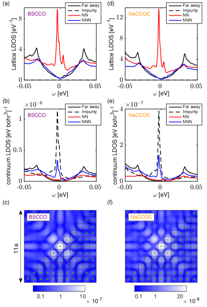
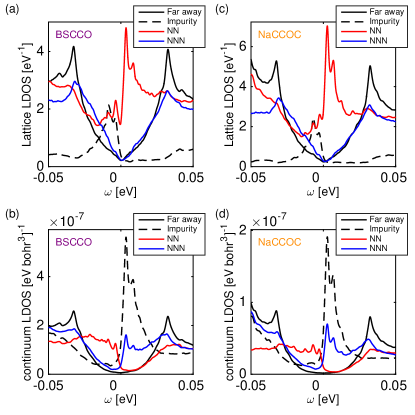
Now, we describe the effects of a strong potential scatterer like Zn in the superconducting state of NaCCOC, and compare it with BSCCO. We use an on-site impurity potential of to model Zn-like potential scatterer. A very similar value to the impurity potential was obtained from the first principles calculations for Zn substituting a Cu atom in BSCCO Kreisel et al. (2015). The effects of correlations are crudely accounted for by scaling down all hopping parameters by a mass renormalization factor for BSCCO (NaCCOC) so that the Fermi velocities match with the corresponding experimental values Damascelli et al. (2003); Zhou et al. (2003). The electron filling is set to , corresponding to optimal doping. The -wave superconductivity is introduced ”by hand” through a pairing interaction on NN bonds with pair potential for BSCCO (NaCCOC), such that a -wave gap with , with meV is obtained for both BSCCO and NaCCOC. Note that the coherence peak positions and therefore the gap maxima are less clear in the tunneling spectra for NaCCOC than for BSCCO; we set the ’s equal only to highlight the other materials-specific differences between the systems that we study here. Fig. 3(a) and (d) show the lattice LDOS in the vicinity of a Zn-like impurity in BSCCO and NaCCOC, respectively. A sharp bound state at is observed in the BSCCO (NaCCOC) lattice LDOS spectrum at the NN site, whereas the lattice LDOS at the impurity site is completely suppressed, as one would expect from a strong impurity. As pointed out in Ref. Kreisel et al., 2015 and illustrated in Fig. 3(b) and (c), the experimentally observed Pan et al. (2000) spatial distribution of spectrum in Zn-doped BSCCO is recovered in the continuum LDOS, obtained at a height Å above the BiO surface using Eq. 12, which shows a sharp peak at directly above the impurity site, and large intensity at the central and NNN sites in the spatial map at this resonance energy. More importantly for the focus of this paper, the impurity-induced states in NaCCOC should follow the same pattern, as illustrated in Fig. 3(e) and (f). This is due to the fact that the Wannier function cut at heights a few Angstroms above the surface (BiO layer in BSCCO and Cl layer in NaCCOC) in both materials are qualitatively very similar, in spite of different surface atoms. While to our knowledge there are no experiments on Zn impurities in NaCCOC, the BdG+W calculations predict that Zn in that system should give rise to the same patterns of impurity-induced states as that in BSCCO.
The qualitative difference between lattice LDOS and continuum LDOS is not only visible in the vicinity of the impurity, but also at sites far from the impurity where a more -shaped spectrum (see Fig. 3(b) and (e)) than seen in the usual -shaped lattice LDOS (see Fig. 3(a) and (d)) is found. This unusual -shaped behavior is actually observed in various STM experiments on the overdoped cuprates Pan et al. (2001); Kohsaka et al. (2008); McElroy et al. (2005); Alldredge et al. (2008); Lang et al. (2002). As discussed in detail in the Appendix, this change of low-energy spectrum can be attributed to the particular form of the Wannier function which vanishes directly above the central Cu site (-wave symmetry) and attains its largest value at the NN sites, see Fig. 2 (d), (h). A simple calculation (see Appendix) shows that the low-energy continuum LDOS spectrum above a Cu site, at heights a few Angstroms above the surface, varies as yielding a more -shaped structure. The suppression of the linear- term can be traced back to the occurrence of nonlocal contributions to the continuum Green’s functionChoubey et al. (2017). It is interesting to speculate why STM data seems to indicate a crossover from -shaped (overdoped) to -shaped (underdoped), possibly related to the variation of the range of the Wannier function as correlations growKkadzielawa et al. (2013), but we have not arrived at a completely satisfactory description of this effect. In any case, the current calculations are applicable only to the more weakly-correlated (overdoped) regime.
So far, we have discussed the calculation of the differential conductance following Eq. (11) by evaluating the continuum LDOS at fixed height above the surface. Experimentally, the differential conductance maps are usually taken in topographic mode, i.e. while scanning the STM tip over an area by keeping the current at a given bias voltage constant such that the height varies with the position Pan et al. (2000); Hudson et al. (2001); Hanaguri et al. (2007); Feenstra (1994). Theoretically, we can simulate a topograph by solving the equationChoubey et al. (2014)
| (15) |
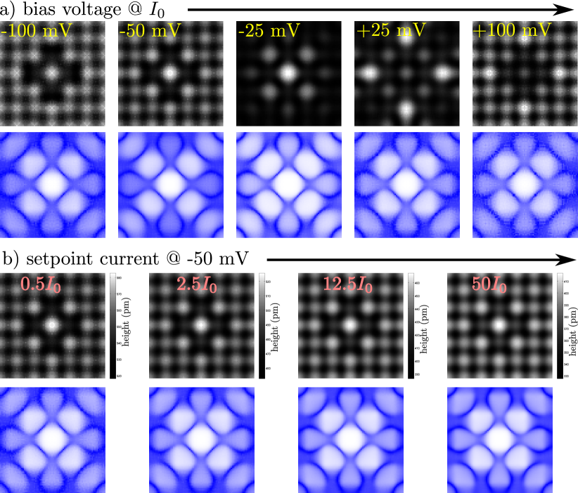
for the height map for given and . Indeed, this requires the calculation of the continuum LDOS within a height range and for all energies to carry out the integral. Since we find little difference in the results between the BdG approach and a T-matrix calculation for the relevant quantities (see Appendix), these calculations have been done with the less computationally expensive T-matrix approach only, as outlined in section III.1. For the strong potential scatterer eV, the calculation of topographs has been carried out for NaCCOC only, with the result as presented in Fig. 4 where in the top rows black and white topographic maps are shown for a fixed current but with varying setpoint voltage (a) and for a fixed setpoint voltage with varying current over several orders of magnitude (b). Indeed, the topographs change with the setpoint bias , since the integral in Eq. (15) is dominated by the real space structure of the impurity resonance at negative energies for mV and at positive energies for mV while at large bias voltage (positive or negative) a larger part of the tunneling current comes from electronic states that are dominated by normal state features. The topographs for fixed current bias voltage but varying current (as shown in Fig. 4(b)), are very similar except that the overall height is moved down when increasing the current. This is a property of the continuum LDOS and consequently the simulated tunneling conductance being in the exponential limitKreisel et al. (2015). With the simulated height map in hand, we can also simulate topographic conductance maps as measured in experiment by using . For each topography in Fig. 4, we also show the topographic conductance maps at the resonance energy with the result that differences are visible in the relative height of the features at the positions above the NN, NNN and NNNN Cu atoms, a consequence of the STM tip being closer to the surface or further away depending on the choice of the setpoint voltage .
IV.3 Effects of a magnetic impurity
We now study magnetic impurity-induced states induced by Ni in BSCCO and NaCCOC. Theoretical results on both materials show very similar behavior due to similar tight-binding parameters and Wannier functions. Ni is known to be a weaker impurity than Zn as it does not disrupt superconductivity in its vicinity, and the pure magnetic scattering is thought to be sub-dominant to the pure potential scattering Hudson et al. (2001). In the absence of magnetic scattering, the resonance peaks are spin degenerate. A small on-site exchange coupling lifts this degeneracy as the effective impurity potential experienced by the electrons becomes spin-dependent , and leads to two spin polarized in-gap resonance states.
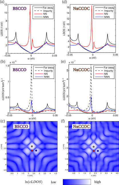
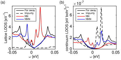
Accordingly, in the simplest scenario, we model Ni as a completely local impurity, with on-site potential eV and exchange coupling , placed in the center of a lattice. Figures 5(a) and (c) show the lattice LDOS spectrum at different sites around such an impurity in BSCCO and NaCCOC, respectively. For BSCCO (NaCCOC), impurity induced resonance peaks at meV and meV are easily observed in the LDOS spectrum at the impurity site and its NN. Resonance peaks at and have down-spin polarization whereas those at and have up-spin polarization. By contrast, the spectrum at the NNN site simply follows the bulk LDOS spectrum. The particular values of and have been chosen just to clearly demonstrate the spin-splitting of impurity-induced resonance peaks due to on-site magnetic scattering. The experimentally observed sharp resonance peaks close to the gap edge Hudson et al. (2001) can not be reproduced in this simple model, due to significant broadening of peaks close to the gap edgeBalatsky et al. (2006).
In order to directly compare with the STM conductance Hudson et al. (2001), we must calculate the continuum LDOS at a typical STM tip position. Figures 5(b) and (d) show the continuum LDOS spectrum in BSCCO and NaCCOC, respectively, at Å above the surface at positions which are directly above the impurity, NN site, NNN site, and a distant site. In both materials, similar to the STM resultHudson et al. (2001), the continuum LDOS exhibits a double peak structure at negative (positive) energies at the positions directly above NN site (impurity and NN sites). Note that this trend is completely missing in the lattice LDOS spectrum (Fig. 5(a) and (c)).
Now we turn to the spatial LDOS maps at the resonance energies in BSCCO. Figure 6(a) shows the lattice LDOS map at around impurity in a region comprising unit cells. The vanishing LDOS at the impurity site and maximum at the NN site observed here is completely opposite to the experimental conductance map at reproduced in Fig. 6(c). However, the continuum LDOS map , at a height Å above the BiO plane, shown in Fig. 6(b) compares very well with the experiment. A similar trend holds at the negative energy resonance peak. The continuum LDOS map at shown in Fig. 6(e) shows excellent agreement with the experimental conductance map at reproduced in Fig. 6(f). The continuum LDOS maps at () is found to be very similar to that at ().
Finally, we note that even though the simple on-site magnetic impurity model captures the spin-splitting of impurity resonance peaks and yields correct spatial patterns of LDOS, a careful comparison with the STM conductance spectrum shows that the relative peak heights are reversed. The experimentally observed relative peak heights can not be explained by an on-site magnetic impurity model as the height of the resonance peak decreases and width increases as it moves away from the mid-gap due to increasing hybridization between bulk and impurity states Balatsky et al. (2006). In the Appendix, we show that an extended impurity model can yield the experimentally observed relative peak heights, and retain the same continuum LDOS patterns.
V Conclusions
In this work, we have tackled the long-standing question of why STM on cuprate surfaces is apparently universal, despite the fact that chemically quite different barrier layers tend to separate the CuO2 plane from the STM tip above the surface. Using a recently developed Wannier-based treatment of the local electronic structure combined with -wave superconductivity, we provided a simple explanation of this universality based on the simple form of the Cu Wannier function several Å above the surface at the tip position. We showed that while these functions are completely different in the vicinity of the CuO2 plane and inside the barrier layer for two cuprate systems commonly used in STM, BSCCO and NaCCOC, their tails detected by the STM tip are remarkably similar. This fact alone should lead to the nearly identical charge order patterns observed in both materialsKohsaka et al. (2007), provided of course that the charge ordered states in the CuO2 plane are in fact the same.
To illustrate the effect of this “filtered” tunneling process and how it affects the spatial conductance patterns observed, we presented again some details of the conductance maps and topographs for a Zn impurity in BSCCO, shown earlierKreisel et al. (2015) to provide a remarkably good agreement with the Zn conductance maps observed in STM over many years. As expected from the above discussion, similar calculations for NaCCOC reproduce extremely similar patterns. This represents a prediction for future experiments, since to our knowledge no experiments on Zn in NaCCOC have been performed. In addition, we studied the Ni impurity problem in BSCCO for the first time with the Wannier-based method, obtaining for the BSCCO system conductance maps with extremely good agreement with experimental maps at the resonance energies. Very similar results were obtained for NaCCOC. Some small discrepancies with the height of the two resonances relative to experiment in BSCCO were noted, and discussed in terms of the range of the Ni impurity potential. Similar calculations were presented for NaCCOC, again with similar patterns predicted.
We have furthermore pointed out an interesting problem regarding the low-energy tunneling conductance that has been noted before phenomenologicallySu et al. (2006) but not analyzed microscopically. The -wave form of the Wannier function at the tip position strongly suppresses the linear- bias dependence of the -axis tunneling density of states, leading to a predicted -shaped characteristic. Indeed, data on overdoped cuprates appears to show this behavior, while for underdoped samples a -shaped spectrum is observed. We discussed possible effects that might explain the crossover from - to -shaped spectra in terms of enhanced correlations in the underdoped phase.
The situation with charge order in the two materials is considerably more subtle, and may depend on a deeper understanding of the origins of charge order in both materials. Recent comparison of inhomogeneous stripe-like charge states of the model, dressed with Wannier functions using the current methodChoubey et al. (2017), suggest that these are indeed of universal origin, and appear identical in the two systems because of the simple form of the Wannier functions above the plane. Future analysis of STM data on this important problem in cuprate physics should use the Wannier-based method to ensure accurate conclusions regarding correlations in the CuO2 plane itself.
VI Acknowledgements
The authors wish to acknowledge useful discussions with J.C. Davis, A. Kostin, W. Ku, and P. Sprau. P.C. and P.J.H. were supported by Grant No. NSF-DMR-1407502. B.M.A. acknowledges support from Lundbeckfond fellowship (grant A9318). Work by T.B. was performed at the Center for nanophase Materials Sciences, a DOE Office of Science user facility. and This research used resources of the National Energy Research Scientific Computing Center, a DOE Office of Science User Facility supported by the Office of Science of the U.S. DOE under Contract No. DE-AC02-05CH11231.
Appendix
Homogeneous state continuum LDOS
Transforming to the momentum-space basis, Eq. (13) and (14] lead to the following expression for the continuum LDOS in a homogeneous system.
| (16) |
Here, is the Fourier transform of the Wannier function, and is the spectral function which can be written as.
| (17) |
where , with being the band energy relative to the Fermi level and superconducting gap , and the coherence factors are given as .
For the continuum position above the Cu site, , at heights several Å above the BiO plane, the dominant contribution to comes from the the Wannier function at the nearest neighbor sites (see Fig. 2). Accordingly
| (18) |
where, and are the values of the Wannier function at , and , where is the in-plane lattice constant. The -wave symmetry of the Wannier function dictates that , however, we still keep it to facilitate discussions in following paragraphs. The higher harmonics neglected in Eq. (18) will not qualitatively change our final conclusions regarding the shape of the continuum LDOS spectrum at low energies.
Using Eqs. 16, 17, and 18, we can express the continuum LDOS above a Cu site for as
| (19) |
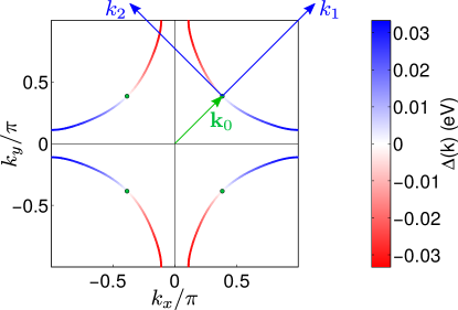
For , the dominant contributions to the above integrals will be from the nodal regions of the Brillouin zone. Accordingly, we shift the origin to the the nodal point , with , and rotate the coordinate axes to and as shown in Fig. 7. Linearizing the band dispersion and gap, we get and where is the Fermi velocity at node and . With these simplifications, in Eq. (19) becomes
| (20) | ||||
where is a circular region around the nodal point with radius , and is the number of nodes. The above integral can be simplified by scaling the coordinates as and , followed by a transformation to the polar coordinates with and , resulting into
| (21) |
Proceeding in a similar manner, we can evaluate as
| (22) |
Finally, turns out to be zero due to vanishing angular integrals. Thus,
| (23) | ||||
The coefficient of the linear in term vanishes as due to symmetry of the Wannier function, however, the coefficient of term is non-zero, and yields a -shaped spectrum at low energies. The equivalent result was obtained earlier using a purely phenomenological model for the hopping between cuprate layersSu et al. (2006). Setting in Eq. (16) [or equivalently , in Eq. (18)] yields the lattice LDOS which, from Eq. (23), turns out to vary linearly with , leading to the well-known -shaped spectrum at low energies.
Details of continuum LDOS spectrum in the vicinity of an impurity
As argued already in the main text, the results for various quantities in presence of an impurity do not significantly depend on whether the T-matrix formalism or the self-consistent BdG method is used. The latter is indeed numerically more demanding because self-consistence in the densities and the superconducting order parameter is required and diagonalization of large matrices is needed. To show explicitly the correspondence of the results, we present in Fig. 8 the same quantities as plotted in Fig. 3, but calculated within the T-matrix formalism. Keeping this in mind, we can safely look at T-matrix results only for the continuum LDOS spectra in the vicinity of a strong impurity.
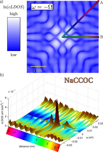
The different shape of the impurity pattern in the continuum LDOS at resonance is also reflected in the spectra taken at different points in real space. For example, if one plots the spectrum along a path away from the impurity, one sees that along the diagonals of the continuum LDOS maps at positive resonance energy , no intensity can be seen, while along the Cu-Cu bond direction, the conductance shows a periodic variation. The situation is different for the conductance at negative resonance energy , where strong variations are seen at the diagonals, and weak variations are seen along the Cu-Cu bonds direction. The same behavior is also demonstrated in Fig. 9 where such a path along the diagonal to the impurity and then along the Cu-Cu bond direction away from the impurity is defined in (a). The spectra along this path as shown in (b) then exhibit periodic modulations of the peak along the diagonal and alternating (decreasing) peaks at and when moving away from the impurity along the Cu-Cu bond direction towards point B.
Normalized conductance maps
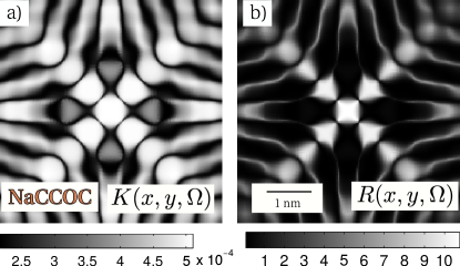
In the main text, we discussed that differential conductance maps slightly depend on the experimental conditions at which the tunneling junction is set up to scan along the surface. A possible way to eliminate this dependence on the experimental parameters ( and ) is to consider the normalized conductanceFeenstra (1994)
| (24) |
which is the ratio of the measured differential conductance and the (at the same time) registered current , normalized by the voltage . As pointed out in Ref. Feenstra, 1994, this quantity is also independent of whether the data has been taken at constant height conditions or constant current conditions (topographic mode) and should be examined in linear scale instead of logarithmic as the conductance maps.
Following our approach for the calculation of differential conductance and current, Eqs. (11) and (15), we can theoretically obtain this quantity
| (25) |
In the exponential limit, the continuum LDOS will have an exponential dependence on the height that dropped out from the formula (25) with the last equal sign, such that it is not necessary to calculate the topographic map . For quantities that are particle-hole symmetric, a similar removal of the setpoint effect can be achieved in to ways: A division of the conductance by the conductance at negative bias yield the quantity
| (26) |
Finally, one can also divide the current at positive bias by the current at negative bias to get
| (27) |
which shows similar features. An example of such a R-map around a strong eV impurity is shown in Fig. 10. The -map is extremely similar.
Extended magnetic impurity model
Although the splitting of peaks due to magnetic scattering is captured in the simple model of a point-like impurity as discussed in section IV.3, a careful comparison with the experimental conductance spectrum shows that the relative heights of the peaks are reversed. In the simple on-site impurity model, the height of the resonance peak decreases and width increases as it moves away from the mid-gap due to increasing hybridization between bulk and impurity states Balatsky et al. (2006). Thus the experimentally observed relative peak heights can not be explained by such model. To this end, we find that an extended impurity model with on-site potential eV, NN potential eV, and NN exchange coupling can lead to the desired trendTang and Flatté (2002); Polkovnikov et al. (2001). This impurity model yields sharp resonance peaks at meV and meV in the lattice and continuum LDOS spectrum as shown in Figure 11(a) and (b), respectively. Clearly, resonance peaks at are higher than those at . Moreover, similar to the experiment and also to the case of on-site impurity model, continuum LDOS shown in Figure 11(b) displays switching of resonance peaks from positive to negative biases and then back to positive biases as one moves from impurity to NN and then to NNN sites. Thus, the extended impurity model captures most of the features of STM results Hudson et al. (2001); however, the microscopic origin of such a model still needs to be investigated.
Details of first principles calculations
The DFT calculations were performed within the generalized gradient approximation (GGA) using the Perdew-Burke-Ernzerhof exchange correlation scheme5 and projector augmented wave potentialsBlöchl (1994) as implemented in VASPKresse and Furthmüller (1996); Kresse and Joubert (1999). We used a 7x7x1 k-point grid and a relatively high kinetic energy cutoff of 2000 eV to ensure high quality Wannier functions. To capture the Wannier functions we projected the Cu- orbital on the bands within [-3,3]eV. Furthermore we used Wannier90Mostofi et al. (2014) in which we set num_iter=0 to retain the correct symmetry of the orbital and dis_num_iter=1000. For the Ca2CuO2Cl2Wannier calculation we set dis_froz_min =-0.9 and dis_froz_max=2.5 to better capture the bands near the Fermi energy. To reduce the two band Wannier function based Hamiltonian of Bi2Sr2CaCu2O8 to a single band Hamiltonian we simply cut the (relatively weak) hopping elements that couple two Cu planes. Atomic and 3D Wannier function images were produced with the VESTA programMomma and Izumi (2011).
References
- Fischer et al. (2007) Øystein Fischer, Martin Kugler, Ivan Maggio-Aprile, Christophe Berthod, and Christoph Renner, “Scanning tunneling spectroscopy of high-temperature superconductors,” Rev. Mod. Phys. 79, 353 (2007).
- Fujita et al. (2012) Kazuhiro Fujita, Andrew R. Schmidt, Eun-Ah Kim, Michael J. Lawler, Dung Hai Lee, J. C. Davis, Hiroshi Eisaki, and Shin-ichi Uchida, “Spectroscopic imaging scanning tunneling microscopy studies of electronic structure in the superconducting and pseudogap phases of cuprate high-Tc superconductors,” J. Phys. Soc. Jpn. 81, 011005 (2012).
- Nieminen et al. (2009) Jouko Nieminen, Ilpo Suominen, R. S. Markiewicz, Hsin Lin, and A. Bansil, “Spectral decomposition and matrix element effects in scanning tunneling spectroscopy of ,” Phys. Rev. B 80, 134509 (2009).
- Balatsky et al. (2006) A. V. Balatsky, I. Vekhter, and Jian-Xin Zhu, “Impurity-induced states in conventional and unconventional superconductors,” Rev. Mod. Phys. 78, 373 (2006).
- Alloul et al. (2009) H. Alloul, J. Bobroff, M. Gabay, and P. J. Hirschfeld, “Defects in correlated metals and superconductors,” Rev. Mod. Phys. 81, 45 (2009).
- Pan et al. (2000) S. H. Pan, E. W. Hudson, K. M. Lang, H. Eisaki, S. Uchida, and J. C. Davis, “Imaging the effects of individual zinc impurity atoms on superconductivity in Bi2Sr2CaCu2O8+δ,” Nature (London) 403, 746 (2000).
- Balatsky et al. (1995) A. V. Balatsky, M. I. Salkola, and A. Rosengren, “Impurity-induced virtual bound states in d-wave superconductors,” Phys. Rev. B 51, 15547 (1995).
- Martin et al. (2002) I. Martin, A. V. Balatsky, and J. Zaanen, “Impurity states and interlayer tunneling in high temperature superconductors,” Phys. Rev. Lett. 88, 097003 (2002).
- Zhu et al. (2000) Jian-Xin Zhu, C. S. Ting, and Chia-Ren Hu, “Effect of unitary impurities on non-STM types of tunneling in high-Tc superconductors,” Phys. Rev. B 62, 6027 (2000).
- Wang et al. (2005) L.-L. Wang, P. J. Hirschfeld, and H.-P. Cheng, “Ab initio calculation of impurity effects in copper oxide materials,” Phys. Rev. B 72, 224516 (2005).
- Choubey et al. (2014) Peayush Choubey, T. Berlijn, A. Kreisel, C. Cao, and P. J. Hirschfeld, “Visualization of atomic-scale phenomena in superconductors: Application to FeSe,” Phys. Rev. B 90, 134520 (2014).
- Kreisel et al. (2015) A. Kreisel, Peayush Choubey, T. Berlijn, W. Ku, B. M. Andersen, and P. J. Hirschfeld, “Interpretation of scanning tunneling quasiparticle interference and impurity states in cuprates,” Phys. Rev. Lett. 114, 217002 (2015).
- Choubey et al. (2017) Peayush Choubey, Wei-Lin Tu, Ting-Kuo Lee, and P. J. Hirschfeld, “Incommensurate charge ordered states in the -- model,” New J. Phys. 19, 013028 (2017).
- Fujita et al. (2014) K. Fujita, Chung Koo Kim, Inhee Lee, Jinho Lee, M. H. Hamidian, I. A. Firmo, S. Mukhopadhyay, H. Eisaki, S. Uchida, M. J. Lawler, E.-A. Kim, and J. C. Davis, “Simultaneous transitions in cuprate momentum-space topology and electronic symmetry breaking,” Science 344, 612 (2014).
- Comin and Damascelli (2016) Riccardo Comin and Andrea Damascelli, “Resonant x-ray scattering studies of charge order in cuprates,” Annu. Rev. Condens. Matter Phys. 7, 369 (2016).
- Hamidian et al. (2016) M. H. Hamidian, S. D. Edkins, Chung Koo Kim, J. C. Davis, A. P. Mackenzie, H. Eisaki, S. Uchida, M. J. Lawler, E.-A. Kim, S. Sachdev, and K. Fujita, “Atomic-scale electronic structure of the cuprate -symmetry form factor density wave state,” Nat. Phys. 12, 150 (2016).
- Kohsaka et al. (2007) Y. Kohsaka, C. Taylor, K. Fujita, A. Schmidt, C. Lupien, T. Hanaguri, M. Azuma, M. Takano, H. Eisaki, H. Takagi, S. Uchida, and J. C. Davis, “An intrinsic bond-centered electronic glass with unidirectional domains in underdoped cuprates,” Science 315, 1380 (2007).
- Hudson et al. (2001) E. W. Hudson, K. M. Lang, V. Madhavan, S. H. Pan, H. Eisaki, S. Uchida, and J. C. Davis, “Interplay of magnetism and high-Tc superconductivity at individual ni impurity atoms in Bi2Sr2CaCu2O8+x,” Nature (London) 411, 920 (2001).
- Salkola et al. (1997) M. I. Salkola, A. V. Balatsky, and J. R. Schrieffer, “Spectral properties of quasiparticle excitations induced by magnetic moments in superconductors,” Phys. Rev. B 55, 12648 (1997).
- Chi et al. (2016) Shun Chi, Ramakrishna Aluru, Udai Raj Singh, Ruixing Liang, Walter N. Hardy, D. A. Bonn, A. Kreisel, Brian M. Andersen, R. Nelson, T. Berlijn, W. Ku, P. J. Hirschfeld, and Peter Wahl, “Impact of iron-site defects on superconductivity in LiFeAs,” Phys. Rev. B 94, 134515 (2016).
- Tersoff and Hamann (1985) J. Tersoff and D. R. Hamann, “Theory of the scanning tunneling microscope,” Phys. Rev. B 31, 805 (1985).
- Hybertsen and Mattheiss (1988) Mark S. Hybertsen and L. F. Mattheiss, “Electronic band structure of CaBi2Sr2Cu2O8,” Phys. Rev. Lett. 60, 1661 (1988).
- Argyriou et al. (1995) D. N. Argyriou, J. D. Jorgensen, R. L. Hitterman, Z. Hiroi, N. Kobayashi, and M. Takano, “Structure and superconductivity without apical oxygens in (Ca,Na,” Phys. Rev. B 51, 8434 (1995).
- Kresse and Furthmüller (1996) G. Kresse and J. Furthmüller, “Efficient iterative schemes for ab initio total-energy calculations using a plane-wave basis set,” Phys. Rev. B 54, 11169 (1996).
- Mostofi et al. (2014) Arash A. Mostofi, Jonathan R. Yates, Giovanni Pizzi, Young-Su Lee, Ivo Souza, David Vanderbilt, and Nicola Marzari, “An updated version of wannier90: A tool for obtaining maximally-localised wannier functions,” Comput. Phys. Commun. 185, 2309 (2014).
- Damascelli et al. (2003) Andrea Damascelli, Zahid Hussain, and Zhi-Xun Shen, “Angle-resolved photoemission studies of the cuprate superconductors,” Rev. Mod. Phys. 75, 473 (2003).
- Zhou et al. (2003) X. J. Zhou, T. Yoshida, A. Lanzara, P. V. Bogdanov, S. A. Kellar, K. M. Shen, W. L. Yang, F. Ronning, T. Sasagawa, T. Kakeshita, T. Noda, H. Eisaki, S. Uchida, C. T. Lin, F. Zhou, J. W. Xiong, W. X. Ti, Z. X. Zhao, A. Fujimori, Z. Hussain, and Z.-X. Shen, “High-temperature superconductors: Universal nodal Fermi velocity,” Nature 423, 398 (2003).
- Pan et al. (2001) S. H. Pan, J. P. O’Neal, R. L. Badzey, C. Chamon, H. Ding, J. R. Engelbrecht, Z. Wang, H. Eisaki, S. Uchida, A. K. Gupta, K.-W. Ng, E. W. Hudson, K. M. Lang, and J. C. Davis, “Microscopic electronic inhomogeneity in the high-Tc superconductor Bi2Sr2CaCu2O8+x,” Nature (London) 413, 282 (2001).
- Kohsaka et al. (2008) Y. Kohsaka, C. Taylor, P. Wahl, A. Schmidt, Jhinhwan Lee, K. Fujita, J. W. Alldredge, K. McElroy, Jinho Lee, H. Eisaki, S. Uchida, D.-H. Lee, and J. C. Davis, “How cooper pairs vanish approaching the mott insulator in Bi2Sr2CaCu2O8+δ,” Nature (London) 454, 1072 (2008).
- McElroy et al. (2005) K. McElroy, D.-H. Lee, J. Hoffman, K. Lang, J. Lee, E. Hudson, H. Eisaki, S. Uchida, and J. Davis, “Coincidence of checkerboard charge order and antinodal state decoherence in strongly underdoped superconducting Bi2Sr2CaCu2O8+x,” Phys. Rev. Lett. 94, 197005 (2005).
- Alldredge et al. (2008) J. W. Alldredge, Jinho Lee, K. McElroy, M. Wang, K. Fujita, Y. Kohsaka, C. Taylor, H. Eisaki, S. Uchida, P. J. Hirschfeld, and J. C. Davis, “Evolution of the electronic excitation spectrum with strongly diminishing hole density in superconducting Bi2Sr2CaCu2O8+δ,” Nat. Phys. 4, 319 (2008).
- Lang et al. (2002) K. M. Lang, V. Madhavan, J. E. Hoffman, E. W. Hudson, H. Eisaki, S. Uchida, and J. C. Davis, “Imaging the granular structure of high-Tc superconductivity in underdoped Bi2Sr2CaCu2O8+x,” Nature (London) 415, 412 (2002).
- Kkadzielawa et al. (2013) Andrzej P. Kkadzielawa, Jozef Spałek, Jan Kurzyk, and Wlodzimierz Wójcik, “Extended hubbard model with renormalized wannier wave functions in the correlated state III,” Eur. Phys. J. B 86, 252 (2013).
- Hanaguri et al. (2007) T. Hanaguri, Y. Kohsaka, J. C. Davis, C. Lupien, I. Yamada, M. Azuma, M. Takano, K. Ohishi, M. Ono, and H. Takagi, “Quasiparticle interference and superconducting gap in Ca2-xNaxCuO2Cl2,” Nat. Phys. 3, 865 (2007).
- Feenstra (1994) R. M. Feenstra, “Tunneling spectroscopy of the (110) surface of direct-gap III-V semiconductors,” Phys. Rev. B 50, 4561 (1994).
- Su et al. (2006) Y. H. Su, H. G. Luo, and T. Xiang, “Universal scaling behavior of the -axis resistivity of high-temperature superconductors,” Phys. Rev. B 73, 134510 (2006).
- Tang and Flatté (2002) Jian-Ming Tang and Michael E. Flatté, “Van hove features in Bi2Sr2CaCu2O8+δ and effective parameters for Ni impurities inferred from stm spectra,” Phys. Rev. B 66, 060504 (2002).
- Polkovnikov et al. (2001) Anatoli Polkovnikov, Subir Sachdev, and Matthias Vojta, “Impurity in a -wave superconductor: Kondo effect and stm spectra,” Phys. Rev. Lett. 86, 296–299 (2001).
- Blöchl (1994) P. E. Blöchl, “Projector augmented-wave method,” Phys. Rev. B 50, 17953 (1994).
- Kresse and Joubert (1999) G. Kresse and D. Joubert, “From ultrasoft pseudopotentials to the projector augmented-wave method,” Phys. Rev. B 59, 1758 (1999).
- Momma and Izumi (2011) Koichi Momma and Fujio Izumi, “VESTA 3 for three-dimensional visualization of crystal, volumetric and morphology data,” J. Appl. Cryst. 44, 1272 (2011).