Dipolar and charged localized excitons in carbon nanotubes
Abstract
We study both experimentally and theoretically the fundamental interplay of exciton localization and polarization in semiconducting single-walled carbon nanotubes. From Stark spectroscopy of individual carbon nanotubes at cryogenic temperatures we identify localized excitons as permanent electric dipoles with dipole moments of up to Å. Moreover, we demonstrate field-effect doping of localized excitons with an additional charge which results in defect-localized trions. Our findings provide not only fundamental insight into the microscopic nature of localized excitons in carbon nanotubes, they also signify their potential for sensing applications and may serve as guidelines for molecular engineering of exciton-localizing quantum dots in other atomically thin semiconductors including transition metal dichalcogenides.
Optical transitions of semiconducting carbon nanotubes (CNTs) are dominated by excitons Wang et al. (2005); Maultzsch et al. (2005) which exhibit strong antibunching in the photoluminescence (PL) in their localized limit Högele et al. (2008). Exciton localization can arise at unintentional defects with shallow potentials Georgi et al. (2010); Hofmann et al. (2016) or incidental proximal charges Tayo and Rotkin (2012) and ensure non-classical emission statistics up to room-temperature Ma et al. (2015a) for excitons bound to deep traps of oxygen side-wall dopants Ghosh et al. (2010); Ma et al. (2014a). Along with oxygen functionalization Ghosh et al. (2010); Ma et al. (2014a, 2015b), covalent side-wall chemistry with aryl and alkyl functionality Piao et al. (2013); Kwon et al. (2016) provides a versatile molecular means to engineer the photophysics of semiconducting CNTs. Introduced in a moderate concentration, the decoration of CNT side-walls with covalent defects results in substantial modifications such as brightening of nanotube emission and increased quantum yields Ghosh et al. (2010); Miyauchi et al. (2013); Piao et al. (2013), axially pinned PL Hartmann et al. (2015) and inhibited diffusion Ma et al. (2014b, 2015c); Hartmann et al. (2016).
Defect-localized excitons in CNTs represent a viable resource for applications in quantum sensing and quantum cryptography. For the latter technology, CNTs may facilitate the development of robust single-photon sources with room-temperature operation in the telecom band by utilizing discrete optical transitions of defect-localized excitons Ma et al. (2015a). Covalent chemistry is readily available to fine-tune the exciton PL energy Ghosh et al. (2010); Ma et al. (2014a, 2015b); Piao et al. (2013); Kwon et al. (2016), and recent successful integration of CNTs into optical cavities Jeantet et al. (2016); Hümmer et al. (2016) has demonstrated Purcell enhancement and directional coupling of single-photon emission as means to increase the single-photon emission efficiency. Moreover, the interplay of chemical modification and charge doping facilitates photoemission from trions Matsunaga et al. (2011); Park et al. (2012); Brozena et al. (2014), which can be utilized to interface photons with the CNT spin degree of freedom Galland and Imamoglu (2008) via schemes of spin-tagged optical transitions analogous to charged semiconductor quantum dots and nitrogen vacancy (NV) centers in diamond Gao et al. (2015). This spin-photon interface in turn should enable all-optical sensing of magnetic fields in analogy to magnetometry based on charged NV color centers Maze et al. (2008); Balasubramanian et al. (2008). A corresponding nanoscale sensor for the measurement of the electric field Vamivakas et al. (2011) with sensitivity down to the elementary electron charge Houel et al. (2012); Hauck et al. (2014) could utilize the electric dipole moment associated with localized excitons.
Our work identifies both integral elements - dipolar localized excitons and voltage-controlled trions - for the development of sensing devices based on carbon nanotubes. By embedding CNTs in a field-effect (FET) device, we performed Stark spectroscopy of localized nanotube excitons in a transverse electric field at cryogenic temperatures. Our experiments demonstrate that exciton localization is accompanied by static exciton polarization irrespective of the details of the localizing potential. An average localization-induced electric dipole moment of Å found experimentally is in good quantitative agreement with ab-initio model calculations for excitons bound by oxygen defects on the side-wall of a nanotube. Moreover, we found that defect potential traps can bind an additional charge to promote PL from defect-localized trions Mouri et al. (2013); Brozena et al. (2014), with control over the charging state provided by the gate voltage.
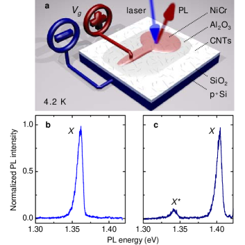
To subject nanotubes to a transverse electric field we fabricated FET devices based on a metal-oxide-semiconductor sequence as illustrated in Fig. 1a. The FET devices were fabricated starting with a doped silicon back gate terminated by an insulating layer of nm thermal SiO2 that was cleaned with standard solvents and subsequently exposed to an oxygen plasma before spin-coating micelle-encapsulated CoMoCat CNTs with a spatial density below m-2. The CNT layer was subsequently covered by sputter deposition with an insulating layer of Al2O3 of variable thickness (with , , and nm in four different sample layouts), and a semitransparent NiCr layer of nm thickness. A gate voltage applied between the top and the ground electrode resulted in a homogeneous transverse electric field through , with being the total thickness of the oxide layers. The functionality of our FET devices with break-down voltages of V at low temperatures, corresponding to transverse electric field strengths of up to , was confirmed with capacitance-voltage spectroscopy SI .
Individual CNTs embedded in a FET device were studied with photoluminescence (PL) spectroscopy in a home-built confocal microscope at the temperature of liquid helium of K. A Ti:sapphire laser tuned in the range of nm was used to excite the PL via phonon sidebands in continuous wave mode. The PL of individual CNTs was dispersed with a monochromator and recorded with a low-noise nitrogen-cooled silicon CCD. Our experiments focused on and chiral nanotubes with emission in the spectral range of eV Bachilo et al. (2003). Characteristic PL signatures of individual nanotubes in our device are shown in Fig. 1b and c. Most of the CNTs were found to exhibit either a single-peak PL emission with an asymmetric lineshape (labelled as in Fig. 1b) characteristic of disorder-localized excitons Galland et al. (2008); Vialla et al. (2014) or a two-peak emission spectrum (denoted as and in Fig. 1c). In our experiments, we assign one-peak spectra to excitons localized by environmental disorder, and two-peak spectra to exciton PL from oxygen-dopant sites introduced on CNT side-walls by sputter deposition of Al2O3 Ma et al. (2015b).
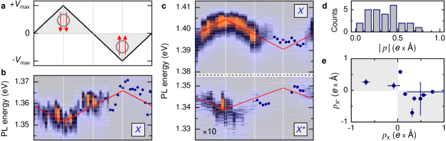
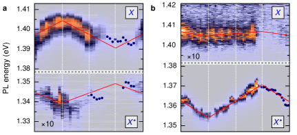
The evolution of the CNT spectra with a single-peak and a double-peak spectrum as a function of the transverse electric field are shown in Fig. 2b and c, respectively. The electric field strength and orientation was varied proportional to the zig-zag voltage ramp shown in Fig. 2a. The gate voltage was changed in discrete steps between maximum positive and negative values, with ranging between V and V depending on the device. After each voltage step a PL spectrum was acquired for an incremental build-up of PL intensity false-color plots as in Fig. 2b for a single-peak emission, and in Fig. 2c for the and peaks. We repeated this procedure on more than 50 individual CNTs. Roughly one third of the tubes we have investigated showed irregular responses such as non-monotonic energy jumps or irreversible intensity fluctuations and were discarded from further analysis. The more regular responses as in Fig. 2b and c are representative for CNT excitons localized by incidental and oxygen-specific defect traps, respectively.
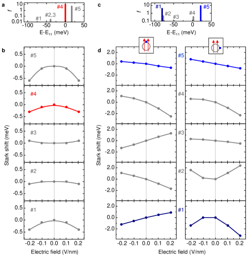
The vast majority of the nanotubes in our devices exhibited linear energy dispersions in response to the transverse electric field ramp, and both blue- and red-shifts were observed SI for different peaks (Fig. 2b and c). The linear slope, associated with the first-order Stark response of a permanent dipole, is in striking contrast to the second-order Stark effect expected for pristine CNTs. From a fitting procedure of CNT PL with single- and double-peak emission spectra as a function of the electric field strength according to (red solid lines in Fig. 2b and c) we extracted the transverse dipole moment of localized excitons with emission energy at V. For the CNT in Fig. 2b, we obtained , and for the two states and of Fig. 2c we determined and from linear fits to the data.
The results of the fitting procedure for all other CNTs with single- and double-peak emission are summarized in the histogram of Fig. 2d. It shows the distribution of the absolute value of the transverse permanent dipole moments determined for different CNTs and devices. The maximum value of the distribution at corresponds to an electron-hole separation of of the CNT diameter, a remarkably large value for a permanent dipole moment that is absent in pristine CNTs according to symmetry considerations. Another remarkable trend in our data are the anti-correlated signs of the dipole moments associated with and peaks (data points within the grey-shaded quadrants in Fig. 2e). Among the tubes with two-peak spectra, the majority exhibited positive and negative permanent dipole values (corresponding to data points in the lower right quadrant).
Our experimental observations suggest an intimate interplay of exciton localization and polarization which we confirmed by atomistic calculations of a model nanotube in transverse electric field SI . In our calculations, the nanotube was embedded in a homogeneous medium with permittivity to account for the effective dielectric environment composed of Al2O3 () and Si2O2 () layers at the top and bottom of the tube and micellar encapsulation. First, we modelled the response of a pristine tube and found a quadratic energy dispersion of the bright luminescent state with transverse polarizability in accord with previous estimates both from tight-binding Benedict et al. (1995); Li et al. (2003); Novikov and Levitov (2006) and first-principles calculations Guo et al. (2004); Brothers et al. (2005); Kozinsky and Marzari (2006).
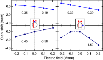
In stark contrast, for both bright peaks associated with an oxygen side-wall defect in ether-d configuration Ma et al. (2014a), our calculations yield predominantly linear dispersions (Fig. 3) when subjected to a transverse electric field of up to V/nm. The slopes and signs depend on the position of the defect on the nanotube side-wall as indicated by inset schematics in Fig. 3. Our calculations predict red- and blue-shifts for the and emission, respectively, with corresponding maximum values for the permanent dipole moments of and for a defect placed at the apex of the tube (left panel of Fig. 3). This defect geometry is expected to dominate our experiments with side-wall dopants introduced preferentially from the top by oxide sputtering, whereas localizing sites at the nanotube base caused by proximal charges Tayo and Rotkin (2012) at the SiO2 surface should be less frequent. Consistently, our experimental data of Fig. 2e reflects both the anti-correlated signs of the two-peak dispersions predicted by theory, and the different likelihood for defects to occur at the top and the bottom of the tubes (in the latter case the respective slopes would remain anti-correlated but interchange their signs). Experimental observation of dispersions as in the right panel of Fig. 3 should be rare because of the peripheral configuration of the related defects in the top-down sputter deposition process.
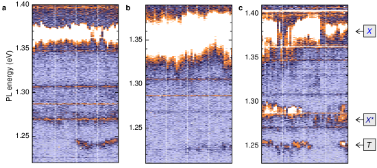
Both experiment and theory suggest that the radial symmetry of the electron-hole charge distribution is imbalanced at the exciton-localizing defect sites by field gradients associated with defect traps, and both the strength and the orientation of the respective dipole moment depend on the specifics of the localizing defect. The defect potentials should also act as traps for individual charges Brozena et al. (2014); Hartmann et al. (2015) and, in the presence of photoexcited electron-hole pairs, give rise to emission from energetically lower-lying trions Matsunaga et al. (2011); Santos et al. (2011); Park et al. (2012); Mouri et al. (2013); Brozena et al. (2014). Indeed, we observed signatures of such red-shifted PL satellites for some nanotubes within limited gate voltage ranges of our devices. Fig. 4a shows the PL response of a CNT to the gate voltage ramp as in Fig. 2a. The PL intensity is represented on a logarithmic false-color scale to enhance the visibility of the weak lowest-energy satellite which we assign to defect-localized trion PL emission (denoted in Fig. 4a as ; the sharp horizontal features unaffected by the gate voltage correspond to Raman scattered laser photons). For this specific tube, the peak was observed around eV in addition to and emission only at negative gate voltages. Other CNTs exhibited similar features only for positive voltages SI indicating that the polarity of the defect excess charge trapped out of the optically excited charge reservoir Santos et al. (2011) depends on the defect potential details. Akin to previous experiments Matsunaga et al. (2011); Santos et al. (2011); Park et al. (2012); Mouri et al. (2013); Brozena et al. (2014), the trion emission emerges at the expense of the main peak PL intensity (compare the relative intensities of and peaks at V and V in Fig. 4b).
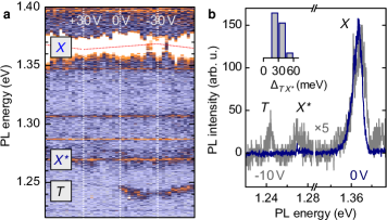
Further confirmation for the assignment of the voltage-induced satellite to trion emission comes from the inspection of the trion binding energy. We extract the energy scale associated with the binding of an excess charge to the lowest defect-localized state by taking the energy splitting between the and emission peaks. This splitting, shown for all CNTs with charging signatures in the inset histogram of Fig. 4b, varies between and meV for the and narrow-diameter tubes in the spectral region of our experiment. This trion binding energy is not to be confused with earlier experiments measuring the splitting between the trion peak and the emission energy with excess contribution from exchange interactions Matsunaga et al. (2011); Santos et al. (2011); Park et al. (2012); Yoshida et al. (2016). It should be rather compared with the theoretical estimate of the bare trion binding energy Ronnow et al. (2009), or with the energy splitting observed between the neutral and charged defect-localized emission peaks in diazonium-functionalized CNTs Brozena et al. (2014). Theory predicts a trion binding energy of about meV for a nanotube in a dielectric medium with Ronnow et al. (2009). In aqueous suspension with , the corresponding experimental value of meV Brozena et al. (2014) was found in accord with the scaling of the trion binding energy with the dielectric constant as Ronnow et al. (2009). Given the relatively high effective dielectric constant of the CNT environment in our FET devices and same diameters of and CNTs, we find very good agreement between our lower values of and theory. Consistently, the larger values in the distribution of Fig. 4b are associated with oxygen-doped nanotubes because of the inverse dependence of the trion binding energy on the tube diameter Ronnow et al. (2009).
Our observation of defect-localized emission in combination with voltage-controlled charging places CNTs alongside semiconductor quantum dots Warburton et al. (2000) and NV centers Gruber et al. (1997) with charge-tunable emission characteristics and spin-projective optical transitions Gao et al. (2015). An intriguing advantage of CNTs for spin-based applications is expected to arise from prolonged electron spin coherence time in an isotopically engineered nuclear-spin free lattice Balasubramanian et al. (2009). Moreover, the absence of dangling bonds in -hybridized CNTs could enable long spin coherence times of electrons localized at engineered nanotube side-wall defects with immediate environmental proximity - a key factor for nanoscale-magnetometry Mamin et al. (2013); Staudacher et al. (2013) where near-surface color centers in diamond currently encounter major limitations due to unsaturated -bonds of the diamond crystal surface Laraoui et al. (2012). Finally, our results could inspire efforts to create chemically engineered quantum dots for in-plane confinement of excitons in emergent two-dimensional transition metal dichalcogenide semiconductors Wang et al. (2012).
We thank J. P. Kotthaus, S. Rotkin, I. Bondarev and V. Perebeinos for useful discussions, P. Altpeter and R. Rath for assistance in the clean room, and P. Stallhofer from Wacker AG for providing the wafer material. This work was performed in part at the Center for Integrated Nanotechnologies, a U.S. Department of Energy, Office of Science user facility. The research was funded by the European Research Council (ERC) under the grant agreement No. 336749 and the Deutsche Forschungsgemeinschaft (DFG) Cluster of Excellence NIM (Nanosystems Initiative Munich) with financial support from the Center for NanoScience (CeNS), LMUinnovativ, and the LANL LDRD program.
References
- Wang et al. (2005) F. Wang, G. Dukovic, L. E. Brus, and T. F. Heinz, Science 308, 838 (2005).
- Maultzsch et al. (2005) J. Maultzsch, R. Pomraenke, S. Reich, E. Chang, D. Prezzi, A. Ruini, E. Molinari, M. S. Strano, C. Thomsen, and C. Lienau, Phys. Rev. B 72, 241402 (2005).
- Högele et al. (2008) A. Högele, C. Galland, M. Winger, and A. Imamoglu, Phys. Rev. Lett. 100, 217401 (2008).
- Georgi et al. (2010) C. Georgi, A. A. Green, M. C. Hersam, and A. Hartschuh, ACS Nano 4, 5914 (2010).
- Hofmann et al. (2016) M. S. Hofmann, J. Noe, A. Kneer, J. J. Crochet, and A. Högele, Nano Lett. 16, 2958 (2016).
- Tayo and Rotkin (2012) B. O. Tayo and S. V. Rotkin, Phys. Rev. B 86, 125431 (2012).
- Ma et al. (2015a) X. Ma, N. F. Hartmann, J. K. S. Baldwin, S. K. Doorn, and H. Htoon, Nat. Nanotechnol. 10, 671 (2015a).
- Ghosh et al. (2010) S. Ghosh, S. M. Bachilo, R. A. Simonette, K. M. Beckingham, and R. B. Weisman, Science 330, 1656 (2010).
- Ma et al. (2014a) X. Ma, L. Adamska, H. Yamaguchi, S. E. Yalcin, S. Tretiak, S. K. Doorn, and H. Htoon, ACS Nano 8, 10782 (2014a).
- Ma et al. (2015b) X. Ma, J. K. Baldwin, N. F. Hartmann, S. K. Doorn, and H. Htoon, Adv. Funct. Mater. 25, 6157 (2015b).
- Piao et al. (2013) Y. Piao, B. Meany, L. R. Powell, N. Valley, H. Kwon, G. C. Schatz, and Y. Wang, Nat Chem 5, 840 (2013).
- Kwon et al. (2016) H. Kwon, A. Furmanchuk, M. Kim, B. Meany, Y. Guo, G. C. Schatz, and Y. Wang, J. Am. Chem. Soc. 131, 6878 (2016).
- Miyauchi et al. (2013) Y. Miyauchi, M. Iwamura, S. Mouri, T. Kawazoe, M. Ohtsu, and K. Matsuda, Nat. Photon. 7, 715 (2013).
- Hartmann et al. (2015) N. F. Hartmann, S. E. Yalcin, L. Adamska, E. H. Hároz, X. Ma, S. Tretiak, H. Htoon, and S. K. Doorn, Nanoscale 7, 20521 (2015).
- Ma et al. (2014b) X. Ma, O. Roslyak, F. Wang, J. G. Duque, A. Piryatinski, S. K. Doorn, and H. Htoon, ACS Nano 8, 10613 (2014b).
- Ma et al. (2015c) X. Ma, O. Roslyak, J. G. Duque, X. Pang, S. K. Doorn, A. Piryatinski, D. H. Dunlap, and H. Htoon, Phys. Rev. Lett. 115, 017401 (2015c).
- Hartmann et al. (2016) N. F. Hartmann, K. A. Velizhanin, E. H. Haroz, M. Kim, X. Ma, Y. Wang, H. Htoon, and S. K. Doorn, ACS nano 10, 8355 (2016).
- Jeantet et al. (2016) A. Jeantet, Y. Chassagneux, C. Raynaud, P. Roussignol, J. S. Lauret, B. Besga, J. Estève, J. Reichel, and C. Voisin, Phys. Rev. Lett. 116, 247402 (2016).
- Hümmer et al. (2016) T. Hümmer, J. Noe, M. S. Hofmann, T. W. Hänsch, A. Högele, and D. Hunger, Nature Communications 7, 12155 (2016).
- Matsunaga et al. (2011) R. Matsunaga, K. Matsuda, and Y. Kanemitsu, Phys. Rev. Lett. 106, 037404 (2011).
- Park et al. (2012) J. S. Park, Y. Hirana, S. Mouri, Y. Miyauchi, N. Nakashima, and K. Matsuda, J. Am. Chem. Soc. 134, 14461 (2012).
- Brozena et al. (2014) A. H. Brozena, J. D. Leeds, Y. Zhang, J. T. Fourkas, and Y. Wang, ACS Nano 8, 4239 (2014).
- Galland and Imamoglu (2008) C. Galland and A. Imamoglu, Phys. Rev. Lett. 101, 157404 (2008).
- Gao et al. (2015) W. B. Gao, A. Imamoglu, H. Bernien, and R. Hanson, Nat Photon 9, 363 (2015).
- Maze et al. (2008) J. R. Maze, P. L. Stanwix, J. S. Hodges, S. Hong, J. M. Taylor, P. Cappellaro, L. Jiang, M. V. G. Dutt, E. Togan, A. S. Zibrov, et al., Nature 455, 644 (2008).
- Balasubramanian et al. (2008) G. Balasubramanian, I. Y. Chan, R. Kolesov, M. Al-Hmoud, J. Tisler, C. Shin, C. Kim, A. Wojcik, P. R. Hemmer, A. Krueger, et al., Nature 455, 648 (2008).
- Vamivakas et al. (2011) A. N. Vamivakas, Y. Zhao, S. Fält, A. Badolato, J. M. Taylor, and M. Atatüre, Phys. Rev. Lett. 107, 166802 (2011).
- Houel et al. (2012) J. Houel, A. V. Kuhlmann, L. Greuter, F. Xue, M. Poggio, B. D. Gerardot, P. A. Dalgarno, A. Badolato, P. M. Petroff, A. Ludwig, et al., Phys. Rev. Lett. 108, 107401 (2012).
- Hauck et al. (2014) M. Hauck, F. Seilmeier, S. E. Beavan, A. Badolato, P. M. Petroff, and A. Högele, Phys. Rev. B 90, 235306 (2014).
- Mouri et al. (2013) S. Mouri, Y. Miyauchi, M. Iwamura, and K. Matsuda, Phys. Rev. B 87, 045408 (2013).
- (31) See supplementary online material for details.
- Bachilo et al. (2003) S. M. Bachilo, L. Balzano, J. E. Herrera, F. Pompeo, D. E. Resasco, and R. B. Weisman, Journal of the American Chemical Society 125, 11186 (2003).
- Galland et al. (2008) C. Galland, A. Högele, H. E. Türeci, and A. Imamoglu, Phys. Rev. Lett. 101, 067402 (2008).
- Vialla et al. (2014) F. Vialla, Y. Chassagneux, R. Ferreira, C. Roquelet, C. Diederichs, G. Cassabois, P. Roussignol, J. S. Lauret, and C. Voisin, Phys. Rev. Lett. 113, 057402 (2014).
- Benedict et al. (1995) L. X. Benedict, S. G. Louie, and M. L. Cohen, Phys. Rev. B 52, 8541 (1995).
- Li et al. (2003) Y. Li, S. V. Rotkin, and U. Ravaioli, Nano Lett. 3, 183 (2003).
- Novikov and Levitov (2006) D. S. Novikov and L. S. Levitov, Phys. Rev. Lett. 96, 036402 (2006).
- Guo et al. (2004) G. Y. Guo, K. C. Chu, D. S. Wang, and C. G. Duan, Phys. Rev. B 69, 205416 (2004).
- Brothers et al. (2005) E. N. Brothers, K. N. Kudin, G. E. Scuseria, and C. W. Bauschlicher, Phys. Rev. B 72, 033402 (2005).
- Kozinsky and Marzari (2006) B. Kozinsky and N. Marzari, Phys. Rev. Lett. 96, 166801 (2006).
- Santos et al. (2011) S. M. Santos, B. Yuma, S. Berciaud, J. Shaver, M. Gallart, P. Gilliot, L. Cognet, and B. Lounis, Phys. Rev. Lett. 107, 187401 (2011).
- Yoshida et al. (2016) M. Yoshida, A. Popert, and Y. K. Kato, Phys. Rev. B 93, 041402 (2016).
- Ronnow et al. (2009) T. F. Ronnow, T. G. Pedersen, and H. D. Cornean, Phys. Lett. A 373, 1478 (2009).
- Warburton et al. (2000) R. J. Warburton, C. Schäflein, D. Haft, F. Bickel, A. Lorke, K. Karrai, J. M. Garcia, W. Schoenfeld, and P. M. Petroff, Nature 405, 926 (2000).
- Gruber et al. (1997) A. Gruber, A. Dräbenstedt, C. Tietz, L. Fleury, J. Wrachtrup, and C. v. Borczyskowski, Science 276, 2012 (1997).
- Balasubramanian et al. (2009) G. Balasubramanian, P. Neumann, D. Twitchen, M. Markham, R. Kolesov, N. Mizuochi, J. Isoya, J. Achard, J. Beck, J. Tissler, et al., Nat. Mater. 8, 383 (2009).
- Mamin et al. (2013) H. J. Mamin, M. Kim, M. H. Sherwood, C. T. Rettner, K. Ohno, D. D. Awschalom, and D. Rugar, Science 339, 557 (2013).
- Staudacher et al. (2013) T. Staudacher, F. Shi, S. Pezzagna, J. Meijer, J. Du, C. A. Meriles, F. Reinhard, and J. Wrachtrup, Science 339, 561 (2013).
- Laraoui et al. (2012) A. Laraoui, J. S. Hodges, and C. A. Meriles, Nano Lett. 12, 3477 (2012).
- Wang et al. (2012) Q. H. Wang, K. Kalantar-Zadeh, A. Kis, J. N. Coleman, and M. S. Strano, Nat. Nanotechnol. 7, 699 (2012).
I Supplementary online material
Field-effect device characteristics
In order to apply transverse electric fields to individual nanotubes we fabricated metal-oxide-semiconductor (MOS) devices as illustrated in Fig. 1a. Highly doped silicon substrate terminated by an insulating layer of nm thermal silicon oxide (SiO2) was used as the ground electrode. The sample surface was cleaned with standard solvents and subsequently exposed to an oxygen plasma. Commercial CoMoCat-nanotubes (SouthWest NanoTechnologies) encapsulated in sodium dodecylbenzenesulfonate (SDS) were dispersed out of an aqueous suspension on SiO2 substrates. The average CNT length was nm, the spin coating parameters were adjusted to yield a CNT density below m-2 which was confirmed by AFM imaging like in Fig. 1a. The CNT layer was subsequently covered with a second insulating layer of aluminum oxide (Al2O3) of variable thickness , yielding a total oxide thickness . A semitransparent top electrode of nm nickel chromium completed the MOS structure.
To determine the strength of the homogeneous electric field in our MOS devices with , , and nm we performed capacitance-voltage (CV) measurements at K. We used a differential CV measurement technique by admixing a sinusoidal modulation voltage with amplitude mV and frequency in the rage of Hz to the dc gate voltage. The resulting ac capacitive current was demodulated with a lock-in amplifier and scaled to the current of a reference capacitance. A representative CV curve recorded for a device with nm is shown in Fig. 1b. At high negative voltages the MOS device response was dominated by hole accumulation where we obtained the maximum capacitance nF in accord with the geometry of our device. For more positive values of the CV curve showed a reduction of the capacitance to without recovery despite further biasing and slow modulation (black CV traces in Fig. 1b), indicating that the limit of strong inversion was suppressed in our device because of slow generation-recombination rates of minority charge carriers at K. This feature as well as the hysteresis at positive are characteristic for non-ideal -type MOS-capacitors with inhibited inversion Sze (1981); Grove et al. (1965) and distinct charging and discharging dynamics of charge traps at the interface Goetzberger. and Irvin (1968). We note, however, that this non-ideal capacitance change as a function of the gate voltage is sufficiently small () to establish a linear relation between the macroscopic electric field strength, , and the gate voltage, , through . With this relation we estimate that field strengths of up to were routinely accessible with voltages of V applied to our devices at low temperatures without break-down.
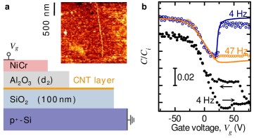
The details of charge traps were investigated with CV spectroscopy with in situ illumination. In the presence of photo-generated electrons by diffuse illumination, inversion was recovered for low-frequency modulation (blue circles in Fig. 1b) as opposed to high-frequency modulation (orange circles in Fig. 1b). From modeling of the CV characteristics in the limiting case of low (high) modulation frequency Grove et al. (1965) shown as blue (orange) solid line in Fig. 1c we determined the characteristic charge impurity density of in our devices. It includes both the surface states at the interface and the charge states in the insulating oxide volume Sze (1981). Devices of different oxide thicknesses were used to determine the volume density of the oxide states, . On average this number implies the presence of a charge trap state within the volume of a cylinder with nm radius around a nm long CNT. These charge traps likely constitute the charge reservoir for photoactivated charge doping of nanotubes that exhibited trion emission.
Stark spectroscopy and trion photoluminescence
Photoluminescence (PL) Stark spectroscopy was performed in response to transverse electric field as detailed in the main text and the Methods section. Individual nanotubes exhibited distinct PL energy shifts according to dipole moments of different defect configurations and geometries. Fig. 2 highlights the case of different responses to a gate voltage ramp as in Fig. 2a of the main text. The data in Fig. 2a is reproduced from Fig. 2c of the main text for direct comparison with another nanotube shown in Fig. 2b with a double-peak spectrum yet different linear Stark shifts of the PL energy. In Fig. 3 we exemplify the response of different individual CNTs to charge doping. Two nanotubes exhibited trion emission satellites at positive gate voltages (Fig. 3a and b) in contrast to a nanotube with similar emission characteristics at zero volts and stable trion emission at negative gate voltages (Fig. 3c).
Quantum chemistry calculations
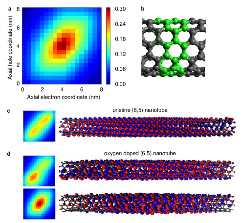
The computations were performed using Gaussian09 software suite Frisch et al. (2015) with B3LYP functional Becke (1988) and STO-3G basis set. The dielectric environment due to silicon oxide and aluminum oxide surroundings of the nanotubes was taken into account as solvent with a dielectric constant of , which is the average dielectric constant of the two oxides. The solvent effects were simulated in the framework of continuum polarizable conductor-like medium Cossi et al. (2003); Barone and Cossi (1998); -nm long segments of (6,5) carbon nanotube with hydrogen-terminated ends were used in these calculations. Pristine and oxygen-doped CNTs were geometry optimized in solvent. The optical transition energies were calculated using Time-Dependent Density Functional Theory (TD-DFT).
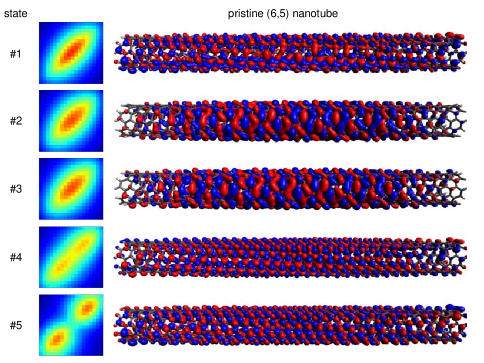
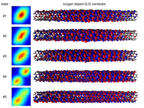
Electric field was applied in transverse direction and optical transition energies were computed without additional geometry optimization. The transition energies, shifted by the energy of transition in pristine CNT, are shown in Fig. 7. In order to establish a quantitative measure of exciton wave functions, exciton plots were built for relevant optical transitions and shown in the left panels of Fig.s 4, 4 and 4 (see Ref.s Mukamel et al. (1997); Tretiak and Mukamel (2002) for more details on exciton plot characterization of excited states in one-dimensional structures). In these contour plots, the bright spot elongated along the diagonal signifies where the exciton wave function is located along the CNT axis, and the ”width” of the elongated plot is the electron-hole correlation length (also referred to as the exciton size). Our analysis shows that excitons are localized on sub- nm length scale (to about nm for the state, denoted as in the main text, and about nm for the state denoted as in the main text) with an electron-hole correlation length of about nm. We also projected the exciton wave function onto the basis of atomic orbitals in order to provide a qualitative real-space visual measure of exciton wave function. The corresponding plots are shown in the right panels of Fig.s 4, 4 and 4.
References
- Sze (1981) S. M. Sze, Physics of Semiconductor Devices (John Wiley & Sons, 1981), 2nd ed.
- Grove et al. (1965) A. Grove, B. Deal, E. Snow, and C. Sah, Solid-State Electronics 8, 145 (1965).
- Goetzberger. and Irvin (1968) A. Goetzberger. and J. C. Irvin, IEEE Trans. Electron Dev. 15, 1009 (1968).
- Frisch et al. (2015) M. Frisch, G. Trucks, H. Schlegel, G. Scuseria, M. Robb, J. Cheeseman, G. Scalmani, V. Barone, B. Mennucci, G. Petersson, et al., Gaussian 09, Revision A. 02; Gaussian, Inc: Wallingford, CT, 2009 (2015).
- Becke (1988) A. D. Becke, Phys. Rev. A 38, 3098 (1988).
- Cossi et al. (2003) M. Cossi, N. Rega, G. Scalmani, and V. Barone, J. Comput. Chem. 24, 669 (2003).
- Barone and Cossi (1998) V. Barone and M. Cossi, J. Phys. Chem. A 102, 1995 (1998).
- Mukamel et al. (1997) S. Mukamel, S. Tretiak, T. Wagersreiter, and V. Chernyak, Science 277, 781 (1997).
- Tretiak and Mukamel (2002) S. Tretiak and S. Mukamel, Chem. Rev. 102, 3171 (2002).