Materials analysis and focused ion beam nanofabrication of topological insulator Bi2Se3
Abstract
Focused ion beam milling allows manipulation of the shape and size of nanostructures to create geometries potentially useful for opto-electronics, thermoelectrics, and quantum computing. We focus on using the ion beam to control the thickness of Bi2Se3 and to create nanowires from larger structures. Changes in the material structure of Bi2Se3 nanomaterials that have been milled using a focused ion beam are presented. In order to characterize the effects of ion beam processing on the samples, we use a variety of techniques including analytical transmission electron microscopy and atomic force microscopy. The results show that while part of the material remains intact after shaping, amorphous regions form where the beam has been used to thin the sample. For wires created by thinning the material down to the substrate, the sidewalls of the wires appear intact based on diffraction images from samples cut at an angle, but thin crystalline regions remain at the wire edges. Even with the resulting defects, focused ion beam milling shows promise for directly fabricating intricate nanodevices of Bi2Se3.
Introduction
In the field of nanoelectronics some of the most interesting device proposals require the control of nanostructure properties, especially the shape and size. In the case of nanodevices made from topological insulators, such as bismuth selenide (Bi2Se3), proposals exist for observing exotic phenomena that could have far-reaching applications, including fault-tolerant quantum computing using Majorana fermions[1, 2, 3, 4, 5, 6, 7] and dramatic increases in thermoelectric efficiency[8, 9, 10, 11, 12, 13]. These proposals require the ability to fabricate structures such as wires with well-controlled dimensions[1, 12], antidot lattices with specific spacings[9, 10], and carefully patterned defects[11, 14, 15]. Directly growing nanotstructures bottom-up into the necessary geometries and defect densities would be ideal, but controlled growth and scaling of such devices is complicated. An alternative is to use top-down methods, such as ion milling, to modify the Bi2Se3[16, 17, 18, 19, 20, 21, 22, 23, 24, 25].
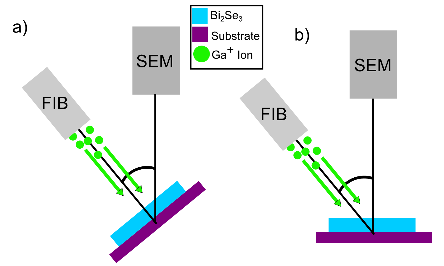
In this article, we focus on the use of gallium-based focused ion beam (FIB) milling, diagramed in Fig. 1. FIB milling utilizes Ga+ ions to sputter away a target material and can be used to both sculpt the material[17, 16, 22, 21] and introduce defects[21, 18]. Recent transport studies have shown that FIB-created nanowires of Bi2Se3 exhibit increased photoconductivity at room temperature[22] and retain signatures of their topological surface states at low temperature[17, 16]. The low-temperature transport results indicate, however, that the nanowires are not entirely Bi2Se3 and that the structure has been partially altered by the FIB[16]. While these results are encouraging for FIB milling as a method of top-down fabrication of Bi2Se3, they do not fully address the materials analysis and changes in the material structure. Therefore, in order to better understand the effects of FIB imaging and modification on Bi2Se3, we have fabricated nanostructures via thinning and cutting with the ion beam and analyzed the material changes. In our study, we combine transmission electron microscopy (TEM) methods—such as energy dispersive x-ray spectroscopy (EDS) and selected area diffraction (SAED)—with atomic force microscopy (AFM).
Results
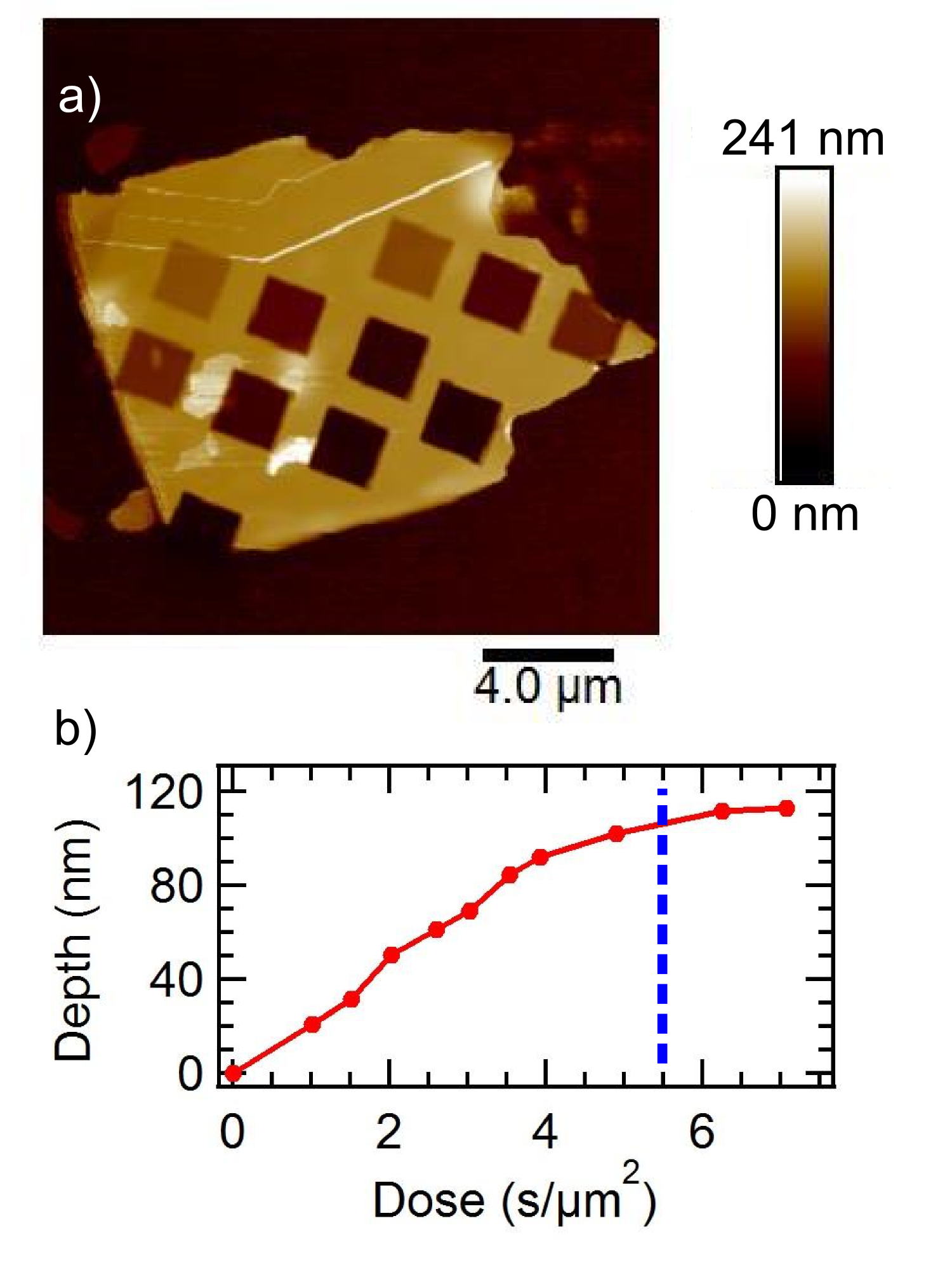
An AFM map of a FIB-milled Bi2Se3 flake on a SiO2 substrate is shown Fig. 2(a). Multiple 4 m2 regions of the flake were exposed to the ion beam, each for a different length of time. The shortest mill time was 4 seconds, and the longest was 28 seconds. All milled regions have a roughness of less than 1 nm, which indicates uniform milling across each area. In comparison, Argon plasma etching[23] creates surfaces with roughness greater than 2 nm for any etch time over a few seconds. Fig. 2(b), which shows the dose in units of seconds per unit area versus etch depth, was calculated from the map in Fig.2(a). The mill-rate appears constant until a depth of 110 nm, which is indicated by a vertical blue dashed line. Below this depth, the FIB had milled beyond the Bi2Se3 and was milling the underlying substrate. The linearity of the mill depth vs. dose before this point suggests that there was minimal sample heating during the exposure times used.
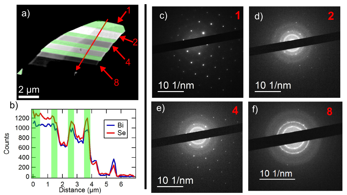
Fig. 3 presents EDS and SAED analysis of a FIB-thinned sample on a silicon nitride TEM window. Fig. 3(a) shows a counts per second image of an exfoliated and milled Bi2Se3 flake. Regions of the flake that were not milled are highlighted in green. The total ion doses used for each region are noted in the Supplement and range from 1015 cm-2 to 2x1016 cm-2. The effect of ion milling on the flake is evident in both the brightness of the stripes in the image and in the x-ray counts in the EDS line scan (path indicated by a red line across the sample in Fig. 3(a)), as shown in Fig. 3(b). The green regions in Fig. 3(b) again denote the unmilled regions. The first milled region, which recieved an ion dose of 1015 cm-2, shows minimal change in Se:Bi count ratio. Regions subjected to higher doses show a decrease in the Se:Bi ratio, which indicates preferential removal of Se. This is expected due to Se’s lower mass. The decrease in the ratio is most extreme in the small amount of leftover material at a horizontal distance 5.5 m from the start of the line scan. At this position, the Bi signal dominates. EDS signatures from Ga were observed only in the areas below region 8, which has been milled down below a thickness of 10 nm. This suggests that the Ga ions largely pass through the Bi2Se3 and become embedded in the silicon nitride. SAED images from several bands across the flake are shown in Fig. 3(c-f). Fig. 3(c) is from the top un-etched region, labeled 1 in Fig. 3(a), and shows a hexagonal diffraction pattern consistent with bulk Bi2Se3. The SAED images from regions 2 and 4, Figs. 3(d) and (e) respectively, show both the hexagonal pattern and a distinct ring with a diameter of 6.3 nm-1. The diffraction pattern from region 8 shows both the 6.3 nm-1 ring and some evidence of polycrystalline Bi2Se3. The polycrystalline structure is indicated by a ring of spots with a diameter of 9.1 nm-1, which corresponds to a lattice spacing of 0.22 nm. The 6.3 nm-1 diameter ring in the milled regions suggests that milling creates an amorphous surface. Given the decrease in the Se:Bi ratio, the surface is likely primarily Bi. The ring diameter equates to a lattice spacing of 0.33 nm, which means the surface could correspond to a bismuth oxide layer formed from air exposure after FIB milling[26, 27] or recrystalized bismuth[28, 29].
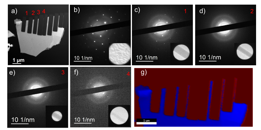
Results from sculpting and milling wires from a flake are presented in Fig. 4. Fig. 4(a) shows a counts per second EDS image of a sample milled to make eight wires of varying widths, from 260 nm to 26 nm. Areas in which the beam etched entirely through the Bi2Se3 and into the silicon nitride appear as lighter gray regions in between the wires. The lighter color is indicative of Ga embedded in the substrate. Elemental maps of the Ga, Se, and Bi in the sample are presented in the Supplement. Numbered 1-4 in the image are wires selected for further analysis. Fig. 4(b) shows the diffraction pattern from the bulk Bi2Se3 region of the flake with the selected area inset. SAED from wires 1-4 are shown in Fig. 4(c-f) respectively, with the selected areas inset. As the wires decrease in width, the Bi2Se3 diffraction spots become more faint. For wire 3 (width 120 nm) only one pair of Bi2Se3 diffraction spots is visible, and for wire 4 (width 26 nm) none are visible. The destruction of the Bi2Se3 as a function of wire width is further evidenced by the EDS elemental mapping shown in Fig. 4(g). In the map, blue areas represent regions containing Bi/Se/Si, and the red areas represent Si only. The Ga signal, while observable in an elemental map, is low enough that the EDS software does not distinguish it in the phase maps. As can be seen in the map, wire 4 is not distinguishable from the substrate. This indicates that although some material remains, as shown in the counts per second image, the wire may no longer be Bi2Se3. This supports what was observed in the diffraction pattern in Fig. 4(f), which shows no evidence of a Bi2Se3 crystal structure. These results are comparable to the transport results in Bhattacharyya et. al.[16]. In the article the authors Ahranov-Bohm oscillations, in FIB-cut nanowires, that show a period associated with wire cross-sections smaller than their physical cross-sections, indicating damage to the wires from the FIB milling. The authors suggested this was due to deformations/cracking or Ga+ ion implantation; our results suggest that the dominant factor is defect creation, which is supported by the minimal Ga signal in the EDS of the thinned sample and by the disappearance of the Bi2Se3 diffraction spots as a function of width in the wires. It should also be noted that we observe no evidence of large scale cracking from the ion milling, which would appear as splitting in the SAED pattern and as visible cracks in the TEM images of the wires.
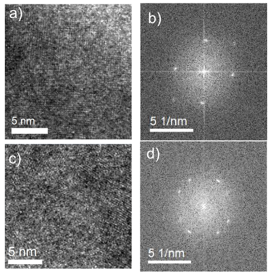
In order to look more carefully at the material along the wire edges and the structure of wire 4, we collected high resolution TEM (HRTEM) images. These images and their fast Fourier transforms (FFT) are shown in Fig. 5. The HRTEM image of the edge of wire 2 is shown in Fig. 5(a) and its FFT is shown in Fig. 5(b). On this edge, only one pair of points in the FFT is associated with the crystal structure of Bi2Se3, while the most prominent pairs indicate a lattice spacing of 0.3 nm. The HRTEM and FFT images of wire 4 are shown in Fig. 5(c) and (d) respectively. Here, there are no observable points associated with Bi2Se3. The dominant structure observed in the wire 4 FFT is the 0.3 nm spacing also found at the edge of wire 2. The FFT of a larger portion of wire 4 is shown in the supplement and does indicate that some of the wire may remain Bi2Se3, but the dominant signal is from the 0.3 nm spacing. This further supports the results from Fig. 4(f) and Fig. 4(g). The FFT and HRTEM images of the wire edges indicate that while some crystal order exists, the edges are largely not Bi2Se3. These images, in particular the results from Fig. 5(a) and (b) suggest that the material at the edge has formed into a cubic structure. This material could be a bismuth oxide[26, 27] or crystalline bismuth[28, 29], similar to that suggested by the thinning results. However, the material by the edge may not directly reflect the edge itself.
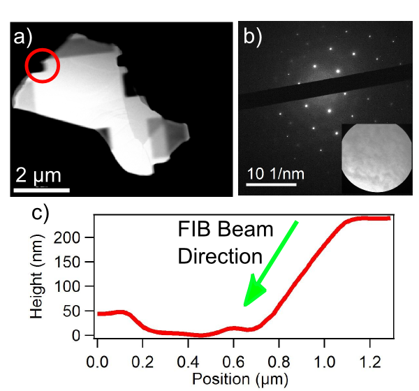
To study the effect of the ion beam on the edges it creates during milling, without the interference of excess material, a sample was milled at an angle. The TEM and AFM results from this sample are shown in Fig. 6. The red circle on the TEM image in Fig. 6(a) highlights the primary analyzed region, though the sample was milled in multiple locations. In this region the beam was incident from right of the sample at an angle of 52∘ from the substrate normal. Fig. 6(b) shows the diffraction from this region, with the selected area shown in the inset. The diffraction pattern from this area is hexagonal and has a lattice parameter of 0.21 nm. Unlike the thinned regions presented in Fig. 3, no amorphous rings appear, which indicates the angle-cut surface is minimally damaged and indistinguishable from un-milled Bi2Se3. In an AFM slice of this region (Fig. 6(c)), we find that the dose from the beam (direction shown by the green arrow), was also able to mill into the silicon nitride window. The surface of the cut is smooth, and the angle of the cut relative to the substrate normal is 58∘. The higher angle of the cut indicates that some material was removed in excess.
Discussion
In conclusion, FIB milling of Bi2Se3 shows promise as method for sculpting this topological insulator to create application-specific geometries. While FIB-thinning the sample creates a uniform and smooth surface, it also damages the material and creates regions that are Se-deficient and partially amorphous. The edges created when cutting wires in the Bi2Se3 are smooth, and their diffraction patterns are indistinguishable from bulk regions. The excess material from direct exposure is shown to be crystalline, but the exact nature of this material was not determinable in this study. The quality of the wires decreased below a width of approximately 150 nm. Smaller wires that maintain the Bi2Se3 crystal may be achievable, however, depending on the characteristics of the FIB tool. Overall, FIB control of Bi2Se3 nanostructures can potentially lead to interesting new physics and applications.
Methods
Nanostructure Transfer
Nanostructures were mechanically exfoliated from bulk Bi2Se3 obtained from Alfa Aesar (99.999% purity). For Bi2Se3 samples on SiO2, they were directly exfoliated onto the substrate. For samples on silicon nitride membranes, the Bi2Se3 was exfoliated onto PMMA, then positioned and transferred onto a 100 nm thick membrane substrate using a micromanipulator and microscope method outlined in Mlack et al.[30]. After positioning, acetone was used to remove the PMMA and complete the transfer of the Bi2Se3 to the membrane. In between all measurements, samples were stored in a vacuum desiccator to reduce the effects of oxidation.
FIB Milling
The samples were milled using a FEI Strata DB235 focused ion beam at 30 kV and 10 pA beam current setting.
TEM Measurement
The samples were analyzed using a JEOL 2010F TEM operating at 200 kV.
AFM Measurement
The AFM was a Brucker Icon atomic force microscope operated in tapping mode.
References
- [1] Ilan, R., Bardarson, J. H., Sim, H.-S. & Moore, J. E. Detecting perfect transmission in josephson junctions on the surface of three dimensional topological insulators. New Journal of Physics 16, 053007, DOI 10.1088/1367-2630/16/5/053007 (2014).
- [2] Fu, L. & Kane, C. L. Superconducting proximity effect and majorana fermions at the surface of a topological insulator. Phys. Rev. Lett. 100, 096407–096411, DOI 10.1103/PhysRevLett.100.096407 (2008).
- [3] Akhmerov, A. R., Nilsson, J. & Beenakker, C. W. J. Electrically detected interferometry of majorana fermions in a topological insulator. Phys. Rev. Lett. 102, 216404, DOI 10.1103/PhysRevLett.102.216404 (2009).
- [4] Hsieh, T. H. & Fu, L. Majorana fermions and exotic surface andreev bound states in topological superconductors: Application to cuxbi2se3. Phys. Rev. Lett. 108, 107005, DOI 10.1103/PhysRevLett.108.107005 (2012).
- [5] Beenakker, C. W. J. Search for majorana fermions in superconductors. In Langer, J. (ed.) Annual Review of Condensed Matter Physics, vol. 4, 113–136 (Annual Reviews, 2013).
- [6] Kitaev, A. Fault-tolerant quantum computation by anyons. Annals of Physics 303, 2 – 30, DOI 10.1016/S0003-4916(02)00018-0 (2003).
- [7] Nayak, C., Simon, S. H., Stern, A., Freedman, M. & Das Sarma, S. Non-abelian anyons and topological quantum computation. Rev. Mod. Phys. 80, 1083–1159, DOI 10.1103/RevModPhys.80.1083 (2008).
- [8] Sun, G. L. et al. Enhanced thermoelectric performance of nanostructured topological insulator bi2se3. Applied Physics Letters 106, DOI 10.1063/1.4907252 (2015).
- [9] Tretiakov, O. A., Abanov, A. & Sinova, J. Thermoelectric efficiency of topological insulators in a magnetic field. Journal of Applied Physics 111, DOI 10.1063/1.3672847 (2012).
- [10] Tretiakov, O. A., Abanov, A. & Sinova, J. Holey topological thermoelectrics. Applied Physics Letters 99, DOI 10.1063/1.3637055 (2011).
- [11] Shi, H., Parker, D., Du, M.-H. & Singh, D. J. Connecting thermoelectric performance and topological-insulator behavior: Bi2te3 and bi2te2se from first principles. Phys. Rev. Applied 3, 014004, DOI 10.1103/PhysRevApplied.3.014004 (2015).
- [12] Shin, H. S. et al. The surface-to-volume ratio: a key parameter in the thermoelectric transport of topological insulator bi2se3 nanowires. Nanoscale 8, 13552–13557, DOI 10.1039/C6NR01716A (2016).
- [13] Wu, K., Ramachandran, B., Kuo, Y., Sankar, R. & Chou, F. Influence of induced defects on transport properties of the bridgman-grown bi2se3-based single crystals. Journal of Alloys and Compounds 682, 225 – 231, DOI 10.1016/j.jallcom.2016.04.306 (2016).
- [14] Sacksteder, V., Ohtsuki, T. & Kobayashi, K. Modification and control of topological insulator surface states using surface disorder. Phys. Rev. Applied 3, 064006, DOI 10.1103/PhysRevApplied.3.064006 (2015).
- [15] Philip, T. M., Hirsbrunner, M. R., Park, M. J. & Gilbert, M. J. Performance of topological insulator interconnects. IEEE Electron Device Letters 38, 138–141, DOI 10.1109/LED.2016.2629760 (2017).
- [16] Bhattacharyya, B. et al. Observation of quantum oscillations in fib fabricated nanowires of topological insulator (bi2se3). Journal of Physics Condensed Matter 29, DOI 10.1088/1361-648X/aa5536 (2017).
- [17] Bhattacharyya, B., Sharma, A., Awana, V., Senguttuvan, T. & Husale, S. Fib synthesis of bi2se3 1d nanowires demonstrating the co-existence of shubnikov-de haas oscillations and linear magnetoresistance. Journal of Physics Condensed Matter 29, DOI 10.1088/1361-648X/29/7/07LT01 (2017).
- [18] Sharma, P. A. et al. Ion beam modification of topological insulator bismuth selenide. Applied Physics Letters 105, DOI 10.1063/1.4904936 (2014).
- [19] Zhou, W., Zhu, H., Valles, C. M. & Yarmoff, J. A. Preparation of clean surfaces and se vacancy formation in bi2se3 by ion bombardment and annealing. Surface Science 662, 67 – 73, DOI 10.1016/j.susc.2017.04.004 (2017).
- [20] Tan, Y. et al. Tailoring nonlinear optical properties of bi2se3 through ion irradiation. Scientific Reports 6, DOI 10.1038/srep21799 (2016).
- [21] Fukui, N. et al. ¡i¿in situ ¡/i¿microfabrication and measurements of bi2se3 ultrathin films in a multichamber system with a focused ion beam, molecular beam epitaxy, and four-tip scanning tunneling microscope. e-Journal of Surface Science and Nanotechnology 12, 423–430, DOI 10.1380/ejssnt.2014.423 (2014).
- [22] Sharma, A., Bhattacharyya, B., Shrivastava, A. K., Senguttuvan, T. D. & Husale, S. High performance broadband photodetector using fabricated nanowires of bismuth selenide. Scientific Reports 6, DOI 10.1038/srep19138 (2016).
- [23] Childres, I., Tian, J., Miotkowski, I. & Chen, Y. Afm and raman studies of topological insulator materials subject to argon plasma etching. Philosophical Magazine 93, 681–689, DOI 10.1080/14786435.2012.728009 (2013).
- [24] Saji, A., Ampili, S., Yang, S.-H., Ku, K. J. & Elizabeth, M. Effects of doping, electron irradiation, h + and he + implantation on the thermoelectric properties of bi2se3 single crystals. Journal of Physics: Condensed Matter 17, 2873, DOI 10.1088/0953-8984/17/19/005 (2005).
- [25] Jia, G., Wu, Z., Wang, P., Yao, J. & Chang, K. Morphological evolution of self-deposition bi2se3 nanosheets by oxygen plasma treatment. Scientific Reports 6, DOI 10.1038/srep22191 (2016).
- [26] Wang, Y., Jiang, L., Tang, D., Liu, F. & Lai, Y. Characterization of porous bismuth oxide (bi2o3) nanoplates prepared by chemical bath deposition and post annealing. RSC Adv. 5, 65591–65594, DOI 10.1039/C5RA09949H (2015).
- [27] In, J. et al. Polymorph-tuned synthesis of and bi2o3 nanowires and determination of their growth direction from polarized raman single nanowire microscopy. Chemistry – A European Journal 17, 1304–1309, DOI 10.1002/chem.201001684 (2011).
- [28] Chen, J., Wu, L.-M. & Chen, L. Syntheses and characterizations of bismuth nanofilms and nanorhombuses by the structure-controlling solventless method. Inorganic Chemistry 46, 586–591, DOI 10.1021/ic0615067 (2007).
- [29] Chang, X. et al. Insights into the growth of bismuth nanoparticles on 2d structured biocl photocatalysts: an in situ tem investigation. Dalton Trans. 44, 15888–15896, DOI 10.1039/C5DT02217G (2015).
- [30] Mlack, J. T. et al. Transfer of monolayer tmd ws2 and raman study of substrate effects. Scientific Reports 7, DOI 10.1038/srep43037 (2017).
Acknowledgments
This work was supported under by the National Science Foundation through the grant EFRI 2-DARE 1542707. Use of University of Pennsylvania Nano/Bio Interface Center instrumentation is acknowledged.
Author contributions statement
J.T.M., S.F., and M.D. devised experiments. J.T.M. and S.F. prepared samples. J.T.M. performed FIB milling. S.F. performed AFM and TEM measurement. J.T.M. analyzed AFM and TEM data and prepared all figures and results discussion. All authors contributed to the manuscript preparation.
Additional information
Competing financial interests: The author(s) declare no competing financial interests.
Figures