Current-induced spin orientation in semiconductors and low-dimensional structures
Abstract
We present here a brief overview of current-induced spin polarization in bulk semiconductors and semiconductor structures of various dimension. The role of band structure and spin relaxation processes is discussed. The related phenomena, such as spin Hall effect, inverse spin Hall effect and other are discussed. Our recent results in this field are presented as well.
Spin-orbit coupling (SOC) is a relativistic effect that provides a link between spin and electric field (including the field of light wave). The SOC is the basis of modern concept of semiconductor spintronics. One can distinguish two main type of the spin orientation at current carrying through the sample: (i) spin Hall effect (SHE), which is the spatial separation of carriers with opposite spins and (ii) homogeneous in the sample polarization. This paper is focused mainly on effect of homogeneous current-induced spin polarization (CISP), however, the related phenomena such as SHE, inverse SHE and other are discussed as well. We will conduct presentation adhering to the chronology of events, which coincides with the transition from bulk semiconductors to low-dimensional ones.
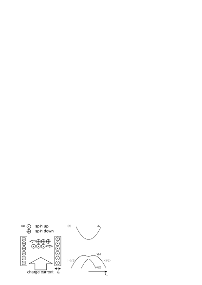
SHE is due to so-called Mott-scattering Mott1965 , known in atomic physics, that is the asymmetry of the scattering relative to the plane determined by momentum and spin that in turn is due to SOC. In semiconductors the role of SOC increases and such an effect is several order of magnitude stronger. In 1971 Dyakonov and Perel predicted this phenomenon in semiconductors Dyakonov1971 ; Dyakonov1971a . The name SHE was introduced later by Hirsch in 1999 Hirsch1999 and the fist experimental observation of SHE was in Awschalom group Kato2004 through more than 30 years after the prediction. The qualitative picture of SHE is depicted in Fig. 1a, where one can see, that the electrons with opposite spin orientation experience the scattering predominantly in opposite directions. This leads to accumulation of carriers with opposite spin projection at opposite sides of the sample at the length scales about spin diffusion length .
The inverse SHE, i.e. the appearance of the dc current due to the nonhomogeneous spin polarization, was predicted by Averkiev and Dyakonov in 1983 Averkiev1983 and detected by Bakun et al. Bakun1984 in the case, when inhomogeneous spin polarization appears due to spin diffusion after interband excitation under condition of optical orientation.
There are two main differences between CISP and SHE: (i) homogeneous vs non-homogeneous spin polarization; (ii) CISP takes place only in gyrotropic semiconductors, while SHE can be realized even in structure with inversion center.
Phenomenologically CISP is described by second rank pseudotensor linking the current density vector and average spin pseudovector
| (1) |
From the symmetry point of view the gyrotropy means that the polar vector (current density) and axial vector (spin) transform under the same irreducible representation. Phenomenological description (1) shows that pseudotensor has non-zero component only if and equally transform under all symmetry operations of the point group of structure. Thus, the relative orientation of spin and current is completely determined by the point group symmetry of the structure. The details of symmetry analysis for frequent two-dimensional (2D) structures one can find e.g. in Ref. Ganichev2014 .
In gyrotropic point symmetry groups there is no difference between components of polar vector (e.g. electric field or current) and axial vector (e.g. magnetic field or spin). The necessary requirement for gyrotropy is the lack of inversion center. However, there is misleading statement, that the gyrotropic crystalls have no reflection planes. Nevertheless, this is too strict requirement, and among 21 classes without spatial inversion only 3 (, and ) are non-gyrotropic, and among the remaining 18 ones only 11 are chiral (have no reflection planes or rotation-reflection axes). The III-V-semiconductors with zinc-blende lattice possess -symmetry and hence are non-gyrotropic, but any symmetry reduction such as strain or dimension lowering leads to CISP. The wurtzite semiconductors (point group ) are initially gyrotropic.
For the first time, the possibility of CISP was proposed for bulk semiconductor tellurium Ivchenko1978 . In this case due to specific band structure (see Fig. 1b), caused by strong SOC, the electric current along trigonal axis leads to non-zero spin oriented in that direction. The effect was detected by means of additional rotation of polarization plane of the light Vorobev1979 .
The carriers acquire the energy in electric field and this process is counterbalanced by scattering, thus, electron distribution is shifted to the following magnitude of quasi-momentum
| (2) |
This anisotropy of carrier distribution leads to uncompensated average spin in non-degenerate in spin band such as tellurium valence band. Here is the electric field and is the momentum relaxation time.
In 2D electron structures the CISP mechanism is sufficiently different from that in tellurium. The conduction band spin-splitting is determined in 2D-structures by the Hamiltonian
| (3) |
where is the effective mass, () are Pauli matrices, () are the components of in-plane wave vector, and components of pseudotensor depend on structure symmetry. From the symmetry point of view the tensors and in Eq. (1) are equivalent.
The first mention on possibility of CISP in 2D-structure due to Rashba spin-splitting Bychkov1984 was in Ref. Vasko1979 . The consistent theory of CISP in 2D-structures was almost simultaneously proposed in Refs. Aronov1989 ; Edelstein1990 . In this connection CISP frequently referred in literature as the Edelstein effect. More complete theory for strained semiconductors and 2D systems was developed in Ref. Aronov1991 . The microscopical calculation of CISP is usually based on the solution of quantum kinetic equation
| (4) |
where is the density matrix, that is diagonal in subband or momentum index, stands for commutator, is the Hamiltonian describing spin-orbit splitting of conduction band (subband), is the collision integral taking into account the processes of elastic scattering. This equation usually can be solved by iterations taking into account the weakness of spin-orbit splitting and electric field. It should be noted, that SOC has to be taken into account in collision integral in contrast to consideration of spin relaxation.
After Aronov1989 ; Edelstein1990 ; Aronov1991 theoretical works extensively reported about CISP in 2D-structures with different symmetry and different types of SOC Chaplik2002 ; Averkiev2005 ; Raichev2007 ; Trushin2007 ; Golub2011 , such as structure inversion asymmetry (SIA) Bychkov1984 due to asymmetry of quantum well (QW) and bulk inversion asymmetry (BIA) Dyakonov1986 that is due to lack of inversion center in semiconductor material Dresselhaus1955 .
The average spin per particle can be estimated as
| (5) |
where is the character energy, that is the temperature in non-degenerate case and the Fermi energy in degenerate one. A parameter depends on specific scattering mechanism.
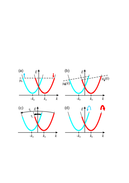
In 2D structures the microscopic mechanism of CISP is other than in tellurium. The three ingredients are necessary for CISP in 2D-system (see Fig. 2): (i) spin-splitting; (ii) electric field, that creates anisotropy of distribution function; (iii) spin relaxation that can be due to -dependent scattering or due to spin precession by Dyakonov-Perel (DP) mechanism Dyakonov1972 .
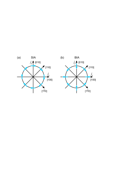
CISP that arises in asymmetric QW due to SIA ( group) is always perpendicular to the current direction (see Fig. 3a), while in the system with BIA ( group) direction of spin polarization crucially depends on the current direction relative to crystal axes as depicted in Fig. 3b. Thus, in [001]-grown QWs the charge current leads to in-plane spin polarization only independently on symmetry of QW, its interfaces and relative contribution of Rashba and Dresselhaus SOC-terms. The magnitude of spin polarization in this case can be up to 5 percent. The out-of-plane spin components can be generated in QW-structures of lower symmetry, e.g. grown in direction [110], [112], [113] etc. The exact relation may be established utilizing the symmetry consideration only.
In significantly high electric field the regime known as ’streaming’ is realized, when the electron accelerates in electric field up to the energy of optic phonon after that phonon is emitted and the process will repeat. The CISP in this case can reach about 2% Golub2013 . Note here another mechanism of CISP: (i) based on spin-dependent scattering even without spin-splitting Tarasenko2006 , (ii) bulk spin polarization generated by the spin Hall current Korenev2006 .
It seems, that CISP has to be more efficient in one-dimensional (1D) systems (quantum wires) due to enhanced relaxation time according to Eqs. (5),(2). However, there is the theorem asserting that in strictly 1D geometry all effects caused by SOC (including CISP) are absent Entin2004 .
Nevertheless, we have recently shown Kokurin2015 that in quasi-1D structure with more than one subband occupied due to possibility of inter-subband scattering CISP is nonzero. For the system with Rashba SOC the simple estimation was found in the case of simple isotropic momentum relaxation
| (6) |
where is the momentum relaxation time in 1D (for simplicity we suppose the same time for intra- and inter-subband scattering), and is the energy between the ground and the first excited quantized subband. This equation differs from that in 2D by replacement [cf. Eq. (5) with from (2)]. Since , but we can conclude that in quasi-1D case the CISP has the efficiency close to that in 2D case.
Another picture can be realized in quasi-1D structures with strong SOC. In this case the spin-splitted subbands with two minima and one maximum (W-shaped) take place, e.g. in InAs-nanowires with tubular electron gas Kokurin2014 ; Kokurin2015a , that resembles the tellurium valence band spectrum. The main difference from tellurium (where extrema of valence band are at side valleys) is the two-fold Kramers degeneracy, because the electrons in mentioned structure are at -point of Brillouin zone. Nevertheless the applied magnetic field lifts above degeneracy and CISP can be separated from equilibrium polarization that is due to applied field. An advantage of InAs-nanowires is the possibility to alter concentration (or position of Fermi energy) by gate, that significantly affect the CISP and average spin has non-monotonic dependence on Fermi energy. Our estimations give close to 10% depending on concentration at reasonable magnitudes of electric field and structure parameters.
Let us now discuss some experimental techniques to measure CISP. In tellurium the electric current applied along -axis leads to spin oriented in the same direction, . In experiment Vorobev1979 the Faraday rotation was utilized to detect the CISP-effect. However, tellurium possesses the natural optical activity, and rotates the polarization plane of linearly polarized light without any electric field or currents. Nevertheless, because of the linear-in-current dependence the CISP-effect was separated by means of inversion of current direction.
In QWs the effect was registered using a circular polarization of photoluminescence at additional non-polarized interband excitation Silov2004 and by Faraday Ganichev2006 or Kerr effect Yang2006 . In Faraday and Kerr effects the rotation of polarization plane is proportional to the spin component along the probe beam. This can complicate the measurement for structure that generates only spin which is normal to the direction of light propagation. However, an applied weak magnetic field rotates the spin that leads to non-zero Faraday (Kerr) signal Kato2004a .
The strong CISP dependence on the crystal axis along which the electric field is applied was detected for [110]-grown QW in Ref. Sih2005 , reflecting the anisotropy of the SOC (SOC contain the term proportional to with ).
In conclusion, we present here the short overview of theoretical and experimental works concerning CISP-effect and some related phenomena. The different mechanisms leading to CISP in semiconductors of various dimensionality are discussed, including specificity of band structure and relaxation features. Our recent results concerning the CISP in quasi-1D systems are presented as well.
Acknowledgement
We are grateful to L.E. Golub for useful discussions. This work was supported by the Government of the Russian Federation (project No. 14.Z50.31.0021 with leading scientist M. Bayer).
References
- (1) N. F. Mott, H. S. W. Massey, The Theory of Atomic Collisions, 3rd Edition, Clarendon Press, Oxford, 1965.
- (2) M. I. Dyakonov, V. I. Perel, Current-induced spin orientation of electrons in semiconductors, Phys. Lett. A 35, 459 (1971). doi:http://dx.doi.org/10.1016/0375-9601(71)90196-4.
- (3) M. I. Dyakonov, V. I. Perel, Possibility of orientating electron spins with current, JETP Lett. 13, 467 (1971).
- (4) J. E. Hirsch, Spin Hall effect, Phys. Rev. Lett. 83, 1834 (1999). doi:10.1103/PhysRevLett.83.1834.
- (5) Y. K. Kato, R. C. Myers, A. C. Gossard, D. D. Awschalom, Observation of the spin Hall effect in semiconductors, Science 306, 1910 (2004). doi:10.1126/science.1105514.
- (6) N. S. Averkiev, M. I. Dyakonov, Sov. Phys. Semicond. 17, 393 (1983).
- (7) A. A. Bakun, B. P. Zakharchenya, A. A. Rogachev, M. N. Tkachuk, V. G. Fleisher, Detection of a surface photocurrent due to electron optical orientation in a semiconductor, JETP Lett. 40, 1293 (1984).
- (8) S. D. Ganichev, L. E. Golub, Interplay of Rashba/Dresselhaus spin splittings probed by photogalvanic spectroscopy - a review, Phys. Status Solidi B 251, 1801 (2014). doi:10.1002/pssb.201350261.
- (9) E. L. Ivchenko, G. E. Pikus, New photogalvanic effect in gyrotropic crystals, JETP Lett. 27, 604 (1978).
- (10) L. E. Vorob’ev, E. L. Ivchenko, G. E. Pikus, I. I. Farbstein, V. A. Shalygin, A. V. Shturbin, Optical activity in tellurium induced by a current, JETP Lett. 29, 441 (1979).
- (11) Y. A. Bychkov, E. I. Rashba, Properties of a 2D electron gas with lifted spectral degeneracy, JETP Lett. 39, 78 (1984).
- (12) F. T. Vasko, N. A. Prima, Sov. Phys. Solid State 21, 994 (1979).
- (13) A. G. Aronov, Y. B. Lyanda-Geller, Nuclear electric resonance and orientation of carrier spins by an electric field, JETP Lett. 50, 431 (1989).
- (14) V. M. Edelstein, Spin polarization of conduction electrons induced by electric current in two-dimensional asymmetric electron systems, Solid State Commun. 73, 233 (1990). doi:http://dx.doi.org/10.1016/0038-1098(90)90963-C.
- (15) A. G. Aronov, Y. B. Lyanda-Geller, G. E. Pikus, Spin polarization of electrons by an electric current, Sov. Phys. JETP 73, 537 (1991).
- (16) A. V. Chaplik, M. V. Entin, L. I. Magarill, Spin orientation of electrons by lateral electric field in 2D system without inversion symmetry, Physica E 13, 744 (2002). doi:http://dx.doi.org/10.1016/S1386-9477(02)00273-4.
- (17) N. S. Averkiev, A. Y. Silov, Circular polarization of luminescence caused by the current in quantum wells, Semiconductors 39, 1323 (2005).
- (18) O. E. Raichev, Frequency dependence of induced spin polarization and spin current in quantum wells, Phys. Rev. B 75, 205340 (2007). doi:10.1103/PhysRevB.75.205340.
- (19) M. Trushin, J. Schliemann, Anisotropic current-induced spin accumulation in the two-dimensional electron gas with spin-orbit coupling, Phys. Rev. B 75, 155323 (2007). doi:10.1103/PhysRevB.75.155323.
- (20) L. E. Golub, E. L. Ivchenko, Spin orientation by electric current in (110) quantum wells, Phys. Rev. B 84, 115303 (2011). doi:10.1103/PhysRevB.84.115303.
- (21) M. I. Dyakonov, V. Y. Kachorovskii, Sov. Phys. Semicond. 20, 110 (1986).
- (22) G. Dresselhaus, Spin-orbit coupling effects in zinc blende structures, Phys. Rev. 100, 580 (1955). doi:10.1103/PhysRev.100.580.
- (23) M. I. Dyakonov, V. I. Perel, Sov. Phys. Solid State 13, 3023 (1972).
- (24) L. E. Golub, E. L. Ivchenko, Spin-dependent phenomena in semiconductors in strong electric fields, New J. Phys. 15, 125003 (2013). doi:10.1088/1367-2630/15/12/125003.
- (25) S. A. Tarasenko, Scattering induced spin orientation and spin currents in gyrotropic structures, JETP Lett. 84, 199 (2006). doi:10.1134/S0021364006160077.
- (26) V. L. Korenev, Bulk electron spin polarization generated by the spin Hall current, Phys. Rev. B 74, 041308 (2006). doi:10.1103/PhysRevB.74.041308.
- (27) M. V. Entin, L. I. Magarill, EPL (Europhy. Letters) 68, 853 (2004). doi:10.1209/epl/i2004-10294-2.
- (28) I. A. Kokurin, N. S. Averkiev, Orientation of electron spins by the current in a quasi-one-dimensional system, JETP Lett. 101, 568 (2015). doi:10.1134/S002136401508007X.
- (29) I. A. Kokurin, Determination of Rashba-coupling strength for surface two-dimensional electron gas in InAs nanowires, Solid State Commun. 195, 49 (2014). doi:http://dx.doi.org/10.1016/j.ssc.2014.07.002.
- (30) I. A. Kokurin, Effect of spin orbit coupling on spectral and transport properties of tubular electron gas in InAs nanowires, Physica E 74, 264 (2015). doi:http://dx.doi.org/10.1016/j.physe.2015.07.003.
- (31) A. Y. Silov, P. A. Blajnov, J. H. Wolter, R. Hey, K. H. Ploog, N. S. Averkiev, Current-induced spin polarization at a single heterojunction, Appl. Phys. Lett. 85, 5929 (2004). doi:http://dx.doi.org/10.1063/1.1833565.
- (32) S. D. Ganichev, S. N. Danilov, P. Schneider, V. V. Bel kov, L. E. Golub, W. Wegscheider, D. Weiss, W. Prettl, Electric current-induced spin orientation in quantum well structures, J. Magn. Magn. Mater. 300, 127 (2006). doi:http://dx.doi.org/10.1016/j.jmmm.2005.10.048.
- (33) C. L. Yang, H. T. He, L. Ding, L. J. Cui, Y. P. Zeng, J. N. Wang, W. K. Ge, Spectral dependence of spin photocurrent and current-induced spin polarization in an InGaAs/InAlAs two-dimensional electron gas, Phys. Rev. Lett. 96, 186605 (2006). doi:10.1103/PhysRevLett.96.186605.
- (34) Y. K. Kato, R. C. Myers, A. C. Gossard, D. D. Awschalom, Current-induced spin polarization in strained semiconductors, Phys. Rev. Lett. 93, 176601 (2004). doi:10.1103/PhysRevLett.93.176601.
- (35) V. Sih, R. C. Myers, Y. K. Kato, W. H. Lau, A. C. Gossard, D. D. Awschalom, Spatial imaging of the spin Hall effect and current-induced polarization in two-dimensional electron gases, Nature Phys. 1, 31 (2005). doi:10.1038/nphys009.