Topological Phase Transition in Layered XIn2P2 (X = Ca, Sr)
00footnotetext: * Corresponding author.
E-mail addresses: wangtao@henannu.edu.cn
Abstract
Based on fully relativistic first-principles calculations, we studied the topological properties of layered XIn2P2 (X = Ca, Sr). Band inversion can be induced by strain without SOC, forming one nodal ring in the kz = 0 plane, which is protected by the coexistence of time-reversal and mirror-reflection symmetry. Including SOC, a substantial band gap is opened along the nodal line and the line-node semimetal would evolve into a topological insulator. These results reveal a category of materials showing quantum phase transition from trivial semiconductor and topologically nontrivial insulator by the tuneable elastic strain engineering. Our investigations provide a new perspective about the formation of topological line-node semimetal under stain.
I INTRODUCTION
Topological insulator(TI) TL1 ; TL2 is a new kind of material possessing gapped bulk states and exotic metallic surface states. The robust surface state in a 3D system, sheltered against backscattering from nonmagnetic impurities as long as the bulk gap remains open and the time-reversal symmetry is preserved serve1 ; serve2 ; serve3 ; serve4 ; serve5 ; serve6 ; serve7 ; serve8 . The unique feature of the surface state has attracted enormous attentions in the theoretical calculations and experimental observations TR3 ; TR4 , not only because of their theoretical importance but also because of their great potential applications app1 ; app2 ; app3 . Recently, the topological properties have been extended into a variety of three dimensional (3D) topological semimetal (TSM) systems pro3 ; pro4 ; pro5 ; pro6 ; pro7 . In most Weyl/Dirac semimetals, conduction bands overlap with valence bands at certain momentum points. For instance, the topological properties of Na3Bi Na1 ; Na2 and Cd2As3 Ta1 ; Ta2 semimetals have been experimentally confirmed. However, in line-node semimetals, the band crossing points around the Fermi level (EF) form a closed loop. Many systems have been proposed as line-node semimetals included Mackay-Terrones crystal (MTC) MTC , Bernal stacked graphene bilayer C , antiperovskite Cu3PdN CuPdN and so on. Such line-node band structure has been measured by the angle-resolved photoelectron spectroscopy (ARPES) in PbTaSe2 exe2 and ZrSiS exe3 . Interestingly, in addition to these materials, researchers also found node line structures in the photonics crystals pho and spin liquids liq . The line-node material is becoming a hot topic.
The topological line-node semimetal could be driven into 3D TI or Dirac semimetal by the SOC and strain. For example, CaTe Ca is a TSM, possessing the nodal rings without SOC, exhibiting Dirac semimetal behavior when SOC is included. When it was applied by appropriate strain, it becomes a strong topological insulator Ca . However, the CaAgX (X = P, As) can be driven into a Tl phase from line-node semimetal by taking into account of SOC Ag .
Bulk CaIn2P2 and SrIn2P2 are layered semiconductors with indirect-gap and direct-gap respectively. They have been investigated with their electronic and optical properties opt . Up to now, their topological properties have not been studied. In this study, we find that the indirect-gap semiconductor can be changed into ‘direct’-gap by applying uniaxial strain slightly. Further Increasing strain, the compound undergoes a transition from trivial insulator to a line-node semimetal with a nodal ring in the kz = 0 plane. When SOC is taken into account, the compounds become a nontrivial topological insulator with Z2 index (1,000). Our results provide a new perspective to understand the effect of strain and SOC on the formation of topological line-node semimetal and insulator.
II CRYSTAL STRUCTURE AND METHOD
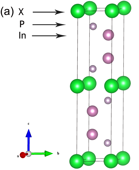
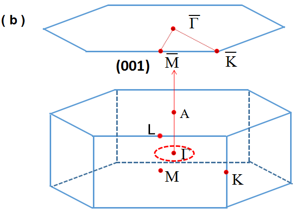
The ternary compound CaIn2P2 is isostructural with SrIn2P2 and crystallizes in a hexagonal structure with the space group P63/mmc struct . The alkaline earth cations X (Ca or Sr) are located at a site with m symmetry; In and P are located at sites with 3m symmetry. The lattice constants of CaIn2P2 and SrIn2P2 are a=b= 4.022 Å, c= 17.408 Åand a=b= 4.094 Å, c= 17.812 Å, respectively exe2 . The corresponding unit cell of the XIn2P2 (X = Ca, Sr) compounds is depicted in Fig.1(a). It contains two chemical formula units, the layers of X2+ cations are separated by [In2P2]2- layers. The atoms positioned at the following Wyckoff positions: X (Ca, Sr): 2a (0, 0, 1/2), In: 4f (2/3, 1/3, 0.329) and P: 4f (1/3, 2/3, 0.396). The bulk Brillouin zone (BZ) and projected surface Brillouin zones of (001) plane are illustrated in Fig.1(b).
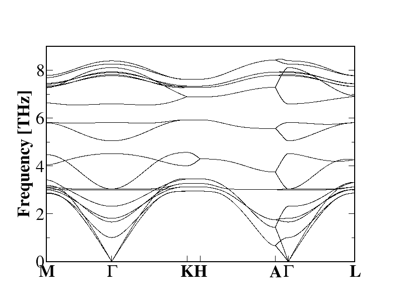
Firstly, we perform density functional calculations by using the WIEN2K package WIEN , with the modified Becke-Johnson exchange potential (mBJ) to get the accurate band gap mbj . The valence configurations of the Ca, Sr, P and In atoms are as Ca , Sr , P and In , respectively. The plane-wave cutoff parameter RMTKmax is set to 7 and a 12 12 3 K-mesh is used for the BZ integral. The SOC interaction is included by using the second-order variational procedure. The tight binding model based on maximally localized Wannier functions (MLWF) method MLWF1 ; MLWF2 has been constructed in order to investigate the surface states. The surface Green’s function of the semi-infinite system, whose imaginary part is the local density of states to obtain the dispersion of the surface states, can be calculated through an iterative methodsancho1984 ; sancho1985 ; wuquansheng . To conform the compounds are dynamicly stable, the phonon spectrum was calculated by using the PHONON code ph .
III Results and discussion
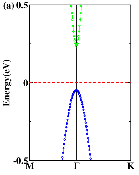
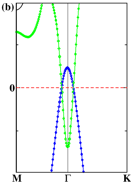
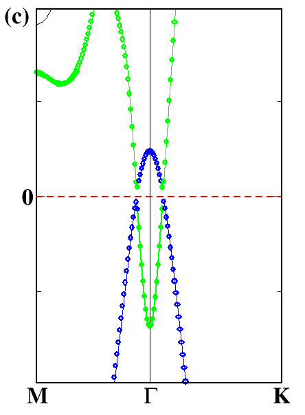
The electronic band structures of the unstrained and 5% strained CaIn2P2 (a/a0=1.05) with SOC are depicted in Fig.2(a) and (b). The unstrained CaIn2P2 has an indirect band gap about 0.5 eV, which agrees with previous studies opt . In Fig.2(a), the 8+ band was pushed down, while the 8- was pushed up, when we induced tensile stress in the a-b plane and compressive stress along c-axis, i.e. increasing a-axis and decreasing c-axis with fixed cell volume. When a1%a0, the compound becomes direct band gap insulator. At the critical point a=2%a0, the 8+ and 8- touch each other. When we further increase a-axis to a=5%a0 the 8+ dropped below 8- band in Fig.2(b). Comparing Fig.2(a) and Fig.2(b), we find that it is the strain rather than the SOC that induces the ‘band-invertion’ PRL108 . From the inset figure in Fig.2(b), we can see a band gap about 35 meV. It is well know that the inversion of bands with opposite parity is a strong indication of the formation of topologically nontrivial phases. This suggests that the strain induces a topological phase transition in CaIn2P2. The band structure of SrIn2P2 has the similar property, excepted its 0.3 eV direct bang gap.
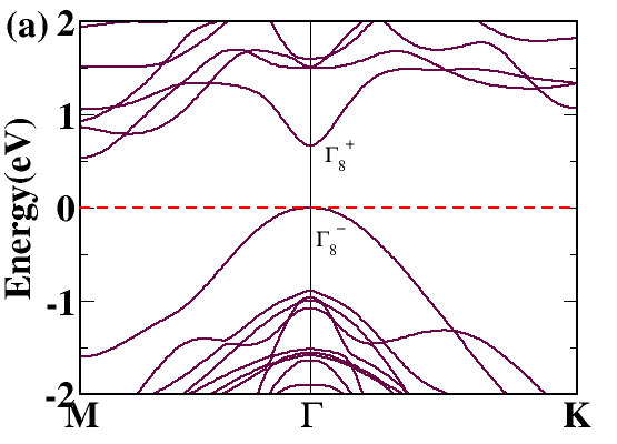
To confirm the topological nature of CaIn2P2, all four Z2 topological invariants (v0; v1 v2 v3 ) Fu were calculated before ( zero strained ) and after ( 5% strained ) the band inversion structures. Following the method developed by Fu and Kane Fu , we calculate directly the Z2 topological invariants from knowledge about the parity of each pair of Kramer’s degenerate occupied energy bands at the eight time-reversal momenta (1, 3M, 1A, and 3L), because of the existence of inversion symmetry in our compounds. Before the band inversion, the products of parities i are identical, yielding a value of zero for all four Z2 topological invariants, i.e., a topologically trivial state (0;000). When the bands with 8+ and 8- symmetries switch around EF, see Figs. 2(a) and 2(b), Γ changes its sign while all other seven i remain unchanged. The parities of time-reversal momenta are listed in Table I. It gives rise to a topological state with Z2 class (1;000) and confirms that the strain induces a topological phase transition.
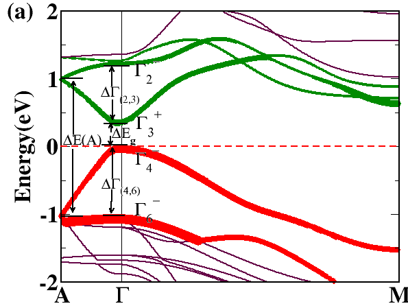
Generally, the band inversion is generated by SOC, formatting the topologically nontrivial state, similar to the prototypical 3D topological insulator Sr2Pb and Bi2Te3 fan1 ; fan2 . However, in our study, the band inversion was induced by the strain only, without considering any SOC. Then, what roles the strain and SOC play in the topological phase transformation of XIn2P2? In Fig.4, we take SrIn2P2 as the example to answer the question. Fig.4 shows the orbital characteristic band structure ( around the and near Fermi energy ) of SrIn2P2 under the different strains. To quantify the effects of strain and SOC on the band inversion in SrIn2P2, we temporally switch off the SOC in Figs.4(a) and 4(b). For the unstrained compound ( Figs.4a ), there is a direct band gap about 0.3 eV, with the In-s state above the P-p state, indicating a trivial topological insulator. When we induce the strain with a=5%a0 and without SOC, the In-s state was pushed down the P-p state, resulting band inversion and line-node band structure ( Fig.4b ). This result indicates that the band inversion is caused by the strain rather than the SOC. For the 5% strained compound, when we include SOC, there is a band gap about 35 meV exactly at the Fermi energy. Comparing the three figures in Fig.4, we can draw the conclusion that lattice strain induces the ‘band inversion’ while SOC opens the band gap.
| M | A | L | Z2 | ||||||||||||||||||||||||||
|---|---|---|---|---|---|---|---|---|---|---|---|---|---|---|---|---|---|---|---|---|---|---|---|---|---|---|---|---|---|
| SOC, strain=0 | + | + | + | + | 0 | ||||||||||||||||||||||||
| SOC, strain=5 | - | + | + | + | 1 |
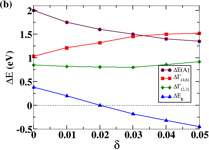
To gain further insight into the mechanism of the strain induced band inversion, we study the electronic structure of unstrained SrIn2P2 around EF in more detail. Without SOC, the projected band structure of SrIn2P2 has been shown in Fig.5(a). It shows that the valence bands 6 and 4 are dominated by the P-pz states, while the conduction bands 2 and 3 are mainly composed of In-s state. Both the valence bands and conduct bands are doubly degenerated at A-point, and they split up into 2-/3+ and 4-/6- bands, respectively. As a result, the 3+ and 4- bands give rise to the conduction band minimum and valence band maximum, respectively. The relative position of the 3+ and 4- bands decides whether a band inversion occurs or not. The energy difference E(A) is determined by the intra-slab covalent s-pz hybridization, while E(4,6) and E(2,3) are related to inter-slab van der Waals pz-pz and s-s interactions. This observation is in line with findings for layered transition metal dichalcogenide semiconductors, such as MoS2 MoS1 ; MoS2 . We have determined the four parameters E(A), E(4,6), E(2,3), and Eg as functions of the uniaxial strain (a-a0)/a0 (volume is fixed). The results are presented in Fig.5(b). With increasing tensile strain in the ab-plane and compressive strain along c-axis, the intra-slab interaction decreases, resulting the increment of the energy spilt E(4,6). However, the inter-slab interaction increase with c-axis decreasing, resulting a strongly reduced E(A), indicating strongly intra-slab covalent s-pz hybridization. The energy level ( derived from P-pz orbit ) increases with c-axis decreasing. So the band gap Eg decreases with the strain increment, and the band gap closes at the critical point =0.02. With further increasing the strain, the band inversion takes place and the compound becomes topological nontrivial line-node semimetal. SOC opens the band gap along the nodal ring and drives the compound into topological nontrivial insulator.
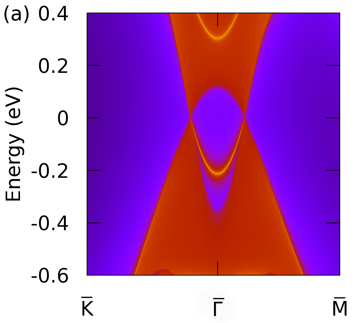
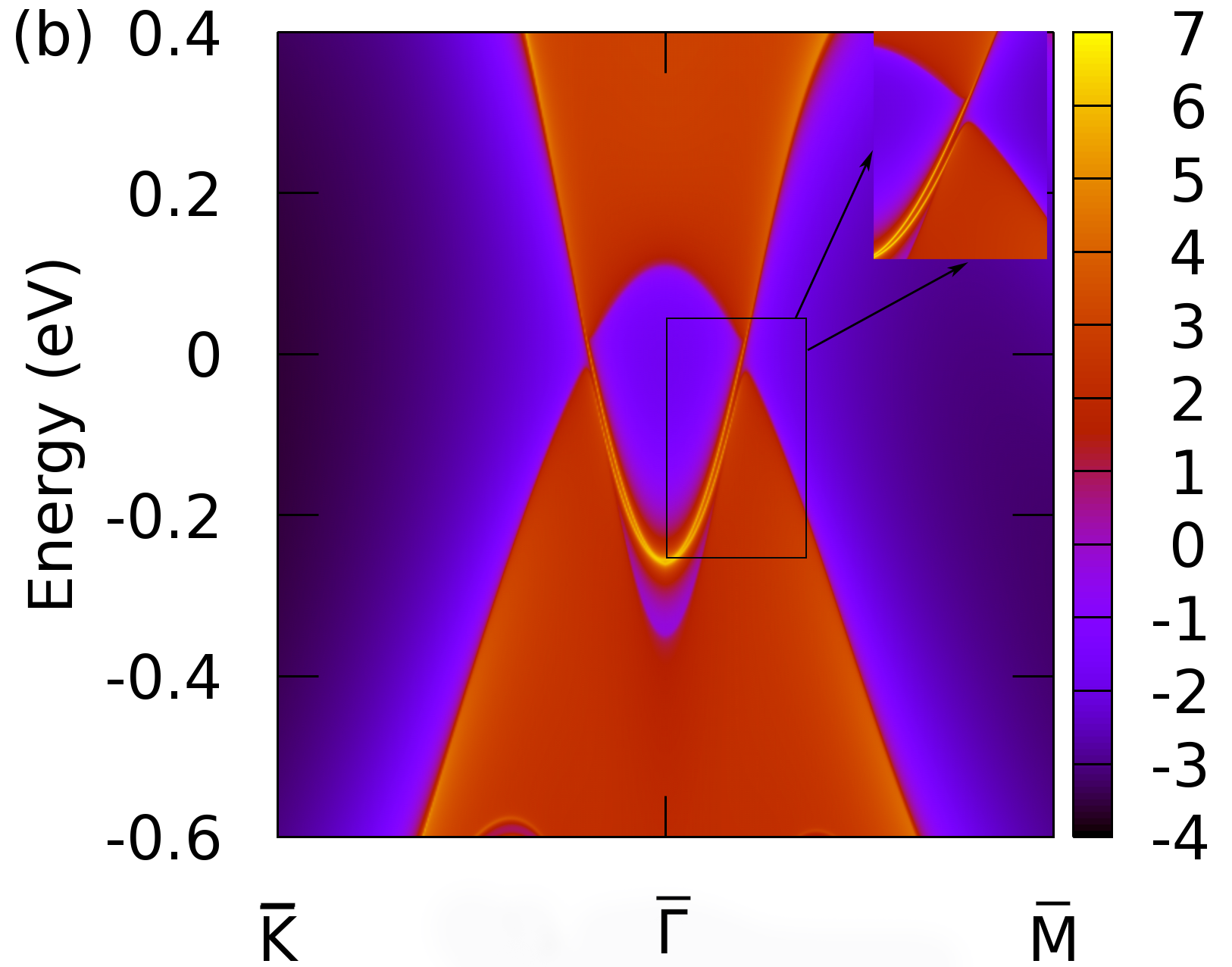
For the topological materials, the existence of the topological prevent surface states is an important character. So we calculate the (001) surface of SrIn2P2 by preforming the WANNIERTOOLS package tool in a tight-binding (TB) scheme based on the maximally localized Wannier functions (MLWFs) MLWF1 . The surface state of Sr2In2P2 (001) surface without and with SOC have been shown in Fig.6(a) and (b), respectively. When SOC is ignored, the system is a line-node semimetal, with the bulk bands touched along , lines and a surface state lining two touching points. This is similar to CaAgAs Ag , protected by the coexistence of time-reversal and mirror-reflection symmetry. When SOC is included, a gap opened at the two touching points, and the compound became an topological nontrivial insulator, with two surfaces states connecting bulk valance and conduction bands (see Fig.6b), coinciding with the previous calculated Z2 ( Table. I).
IV CONCLUSION
In conclusion, by the first-principles calculations, we find the quantum phase transition in XIn2P2 from conventional semiconductor into the line node semimetal by strain engineering only without SOC. While SOC takes the role as opening band gap along the line node and gives rise to the nontrivial topological insulator state.
Acknowledgements.
The authors acknowledge support from the NSF of China (No.11274095, No.10947001) and the Program for Science and Technology Innovation Talents in the Universities of Henan Province (No.2012HASTIT009, No.104200510014, and No.114100510021). This work is supported by The High Performance Computing Center (HPC) of Henan Normal University.References
- (1) J. Moore, Nat. Phys. 5, 378 (2009).
- (2) M. Z. Hasan and C. L. Kane, Rev. Mod. Phys. 82, 3045 (2010).
- (3) M. Z. Hasan and C. L. Kane, Rev. Mod. Phys. 82, 3045 (2010).
- (4) X. L. Qi and S. C. Zhang, Rev. Mod. Phys. 83, 1057 (2011).
- (5) B. A. Bernevig, T. L. Hughes, and S.-C. Zhang, Science 314, 1757 (2006).
- (6) C. L. Kane and E. J. Mele, Phys. Rev. Lett. 95, 226801 (2005).
- (7) H.Zhang,C.-X.Liu,X.-L.Qi,X.Dai,Z.Fang,andS.-C.Zhang, Nat. Phys. 5, 438 (2009).
- (8) K?nig M, Wiedmann S, Brš¹ne C, et al, Science 318, 766 (2007).
- (9) J. Moore, Nat. Phys. 5, 378 (2009).
- (10) X.-L. Qi and S.-C. Zhang, Phys. Today 63, 33 (2010).
- (11) X.-L. Qi and S.-C. Zhang, Phys. Today 63, 33 (2010).
- (12) X.-L. Qi and S.-C. Zhang, Rev. Mod. Phys. 83, 1057 (2011).
- (13) Fu, Liang, and Charles L. Kane, Phys. Rev. Lett. 100, 096407 (2008).
- (14) Qi X L, Hughes T L and Zhang S C Phys. Rev. B, 78, 195424 (2008). Qi X-L, Li R, Zang J and Zhang S-C, Science 323, 1184 (2009).
- (15) Essin A M, Moore J E and Vanderbilt D, Phys. Rev. Lett. 102, 146805 (2009).
- (16) X. Wan, A. M. Turner, A. Vishwanath, and S. Y. Savrasov, Phys. Rev. B 83, 205101 (2011).
- (17) L. Balents, Physics 4, 36 (2011).
- (18) Y. Ando, J. Phys. Soc. of Jpn. 82, 102001 (2013).
- (19) K.-Y. Yang, Y.-M. Lu, and Y. Ran, Phys. Rev. B 84, 075129 (2011).
- (20) T. O. Wehling, A. M. Black-Schaffer, and A. V. Balatsky, Adv. Phys. 63, 1 (2014).
- (21) Z. Wang, Y. Sun, X.-Q. Chen, C. Franchini, G. Xu, H. Weng, X. Dai, and Z. Fang, Phys. Rev. B 85, 195320 (2012).
- (22) Z. K. Liu, B. Zhou, Y. Zhang, Z. J. Wang, H. M. Weng, D. Prabhakaran,S.-K.Mo, Z.X.Shen, Z.Fang, X.Dai, Z.Hussain and Y. L. Chen, Science 343, 864 (2014).
- (23) Z. Wang, H. Weng, Q. Wu, X. Dai, and Z. Fang, Phys. Rev. B 88, 125427 (2013).
- (24) Z. K. Liu, J. Jiang, B. Zhou, Z. J. Wang, Y. Zhang, H. M. Weng, D. Prabhakaran, S.-K. Mo, H. Peng, P. Dudin, T. Kim, M. Hoesch, Z. Fang, X. Dai, Z. X. Shen, D. L. Feng, Z. Hussain, and Y. L. Chen, Nat. Mater. 13, 677 (2014).
- (25) Z. Gao, M. Hua, H. Zhang, and X. Zhang, arXiv:1507.07504.
- (26) J.-W. Rhim and Y. B. Kim, Phys. Rev. B 92, 045126 (2015).
- (27) Yu R, Weng H, Fang Z, et al. Physical review letters, 2015, 115(3): 036807.
- (28) G. Bian, T.-R. Chang, R. Sankar, S.-Y. Xu, H. Zheng, T. Neupert, C.-K. Chiu, S.-M. Huang, G. Chang, I. Belopolski, D. S. Sanchez, M. Neupane, N. Alidoust, C. Liu, B. Wang, C.-C. Lee, H.-T. Jeng, A. Bansil, F. Chou, H. Lin, and M. Zahid Hasan, arXiv:1505.03069.
- (29) L. M. Schoop, M. N. Ali, C. Straer, V. Duppel, S. S. P. Parkin, B. V. Lotsch, and C. R. Ast, arXiv:1509.00861.
- (30) L. Lu, L. Fu, J. D. Joannopoulos, and M. Soljai, Nat. Photonics 7, 294 (2013).
- (31) W. M. H. Natori, E. Miranda, and R. G. Pereira, arXiv:1505.06171.
- (32) Du Y, Tang F, Wang D, et al. arXiv preprint arXiv:1605.07998, 2016.
- (33) Yamakage A, Yamakawa Y, Tanaka Y, et al. Journal of the Physical Society of Japan, 85(1): 013708 (2015).
- (34) Guechi N, Bouhemadou A, Guechi A, et al. Journal of Alloys and Compounds, 577: 587-599 (2013).
- (35) J.F. Rauscher, C.L. Condron, T. Beault, S.M. Kauzlarich, N. Jensen, P. Klavins, S. MaQuilon, Z. Fisk, M.M. Olmstead, Acta Cryst. C 65, 69 (2009).
- (36) P. Blaha, K. Schwarz, G.K.H. Madsen, D. Kvasnicka, and L. Luitz, (Technical University of Vienna, Vienna, 2001).
- (37) F. Tran and P. Blaha, Phys. Rev. Lett. 102, 226401 (2009).
- (38) A. A. Mostofi, J. R. Yates, Y.-S. Lee, I. Souza, D. Vanderbilt, and N. Marzari, Comput. Phys. Commun. 178, 685 (2008).
- (39) N. Marzari, A. A. Mostofi, J. R. Yates, I. Souza, and D. Vanderbilt, Rev. Mod. Phys. 84, 1419 (2012).
- (40) J. M .Sancho, J. Math. Phys., 25(2), 354 (1984).
- (41) J. M. Sancho, Phys. Rev. A 31 (5), 3523 (1985 ).
- (42) G. W. Winkler, Q. S. Wu, et. al,, arxiv:1602.07001; A. Tamai, Q. S. Wu, I. Cucchi, and et. al., Phys. Rev. X 6, 031021 (2016).
- (43) X. Gonze and C. Lee, Phys. Rev. B 55, 10355 (1997).
- (44) Zhu Z, Cheng Y, Schwingenschl?gl U, Physical review letters, 108(26): 266805 (2012).
- (45) L. Fu and C.L. Kane, Phys. Rev. B 76, 045302 (2007).
- (46) H.Zhang, C.-X.Liu, X.-L.Qi, X.Dai, Z.Fang,andS.-C.Zhang, Nat. Phys. 5, 438 (2009).
- (47) Y. Sun, X.-Q. Chen, C. Franchini, D. Li, S. Yunoki, Y. Li, and Z. Fang, Phys. Rev. B 84, 165127 (2011).
- (48) Zhu, Z. Y., Y. C. Cheng, and Udo Schwingenschl?gl., Phys. Rev. B 84, 153402 (2011).
- (49) K.F. Mak, C. Lee, J. Hone, J. Shan, and T.F. Heinz, Phys. Rev. Lett. 105, 136805 (2010).
- (50) Q. S. Wu, https://github.com/quanshengwu/wanniertools (2015).
- (51) N. Kopnin, T. Heikkil, and G. Volovik, Phys. Rev. B 83, 220503 (2011).