Demystifying the Characteristics of 3D-Stacked Memories: A Case Study for Hybrid Memory Cube
Abstract
Three-dimensional (3D)-stacking technology, which enables the integration of DRAM and logic dies, offers high bandwidth and low energy consumption. This technology also empowers new memory designs for executing tasks not traditionally associated with memories. A practical 3D-stacked memory is Hybrid Memory Cube (HMC), which provides significant access bandwidth and low power consumption in a small area. Although several studies have taken advantage of the novel architecture of HMC, its characteristics in terms of latency and bandwidth or their correlation with temperature and power consumption have not been fully explored. This paper is the first, to the best of our knowledge, to characterize the thermal behavior of HMC in a real environment using the AC-510 accelerator and to identify temperature as a new limitation for this state-of-the-art design space. Moreover, besides bandwidth studies, we deconstruct factors that contribute to latency and reveal their sources for high- and low-load accesses. The results of this paper demonstrates essential behaviors and performance bottlenecks for future explorations of packet-switched and 3D-stacked memories.
I Introduction and Motivation
To date, the dominant architecture for computing systems has been the processor-centric architecture, in which the processor and DIMM-based memories are separate units connected via the JEDEC protocol [1]. This architecture inherently enables the use of a large centralized memory accessed by multiple processors. However, the quest for increasing memory bandwidth has led to the development of 3D-DRAM packages and the resulting emergence of on-package, high-bandwidth 3D memory tightly integrated with the processor, two examples of which are High Bandwidth Memory (HBM) [2] and Hybrid Memory Cube (HMC) [3]. While HBM provides high bandwidth on top of the traditional JEDEC-based communication, HMC utilizes modern packet-based interfaces and relies on high degree of internal concurrency. Further, to eliminate costly data movement between the processor and memory subsystems, researchers are exploring the integration of compute units within such high-bandwidth memories (e.g., the integration of CMOS logic and DRAM dies within a 3D stack). This paper reports on experimental characterizations of HMC to provide an understanding of sources of high performance and bottlenecks; and therefore, implications for effective application design for both traditional and processor-in-memory (PIM) configurations.
The novel structure of HMC has motivated researchers to develop architectures based on concepts introduced in HMC [4, 5, 6, 7, 8]. Although many researchers have studied the 3D-stacked layered integration of computation and memory based on simulation, experimental studies are few [9, 10, 11]. In particular, to the best of our knowledge, no experimental work has sought to characterize the relationship between temperature, power consumption, bandwidth, and latency111This paper uses the term latency and round-trip time interchangeably. of these memories. Importantly, in PIM configurations, a sustained operation can eventually lead to failure by exceeding the operational temperature of HMC, assumed to be °C [12, 13]. Furthermore, the physical organization of 3D-stacked memories introduces new structural abstractions with corresponding new latency and bandwidth hierarchies. Therefore, maximizing bandwidth utilization relies on data mappings and associated reference patterns that are well matched to the concurrency of the internal organization of HMC. Our analysis examines the implications of this internal organization on the mapping of data structures in applications.

Characterizations in this paper, as shown in Figure 1, seek to explore and quantify the conceptual relationships between bandwidth, temperature, power consumption, and latency. Figure 1a depicts the first relationship: as bandwidth increases, temperature increases that can eventually exceed the operational range. To mitigate high temperatures, systems must use costlier cooling solutions.222For instance, AMD Radeon R9 Fury X GPU, which integrates an HBM and a GPU on an interposer, requires a liquid cooling solution [14]. Moreover, higher temperatures trigger mechanisms such as frequent refresh [15], which also increases power consumption. Therefore, as Figure 1b depicts, as bandwidth increases, the power consumption of a device and its required cooling power rises. In addition, to determine the benefits of HMC in a system, an integral asset is the relationship between the bandwidth and latency (Figure 1c). Since we use a prototype infrastructure, we deconstruct elements that contribute to latency under low- and high-load utilizations with various bandwidth profiles. We believe that understanding the impact of such elements provides insights about the full-system impact of the HMC in particular, and 3D-stacked memories in systems in general.
To this end, in this paper, we use a system with a controllable cooling system and an AC-510 [16] accelerator board, which includes an HMC 1.1 (Gen2) [15] and an FPGA. On the FPGA, we systematically generate synthetic workloads using customized Verilog implementations based on GUPS (giga updates per second) such as various combinations of high-load, low-load, random, and linear access patterns, which are building blocks of real applications. We analyze the bandwidth, latency, and power consumption of HMC while using a thermal camera to record its temperature. This paper contributes the following: (\romannum1) This is the first study, to the best of our knowledge, that measures the effects of increased bandwidth on temperature and power altogether in a real 3D-stacked memory system and explores the sensitivities to, and consequences of, thermal limits; (\romannum2) it exposes the interactions among bandwidth utilization, power consumption, and access patterns in a real 3D-stacked memory system; (\romannum3) it explores contributing factors to latency and yields insights into why, when, and how HMC benefits applications; and (\romannum4) it presents an analysis of latencies in HMC based on the impact of packet-switched interfaces, and the relationship to the structural organization (i.e., vaults, banks, and quadrants).
II Hybrid Memory Cube
This section introduces the architectural organization, communication interface and protocol, and address space mapping of the HMC. We focus on the HMC 1.1 specification [15] for which the hardware is currently available and used in the experiments described in this paper. We also briefly compare the specification of HMC 2.0 [17], whose hardware is yet to be available, HMC 1.1 (Gen2), and HMC 1.0 (Gen1) [18].
II-A HMC Structure
HMC is a 3D-stacked memory composed of a logic die upon which multiple DRAM layers are stacked. The dies are vertically connected by through-silicon-vias (TSVs), which provide higher internal bandwidth, lower latency, and lower communication energy consumption within a cube than comparable 2D structures [6, 3, 19]. Figure 2 shows the HMC 1.1 structure, composed of one logic layer and eight DRAM layers, each divided into 16 partitions. Accordingly, the 3D stack is divided into 16 vertical vaults [18], each with its own memory controller in the logic layer, connected to DRAM partitions by 32 data TSVs333 Another reference [15] mentions that internally within each vault the granularity of the DRAM data bus is 32 B. reside above it [3].
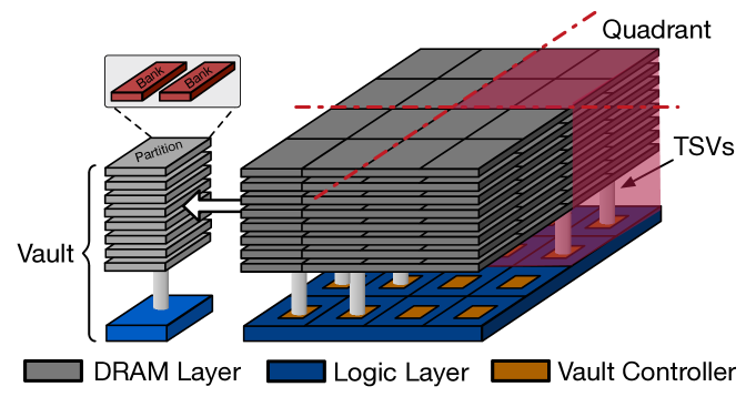
Therefore, in HMC 1.1, each memory controller is responsible for eight partitions of DRAM layers. As shown in the figure, a collection of four vaults is called a quadrant, whose vaults share a single external link.444As shown in Table II-A, each quadrants contains 8 vaults in HMC 2.0. Each DRAM layer in a Gen1 device (HMC 1.0) is a 1 Gb die manufactured in 50 nm technology [3]. Each Gen1 device has four layers of DRAM and the size of a Gen1 device is . Further, each layer is composed of 16 partitions, so the size of each DRAM partition is . In addition, in Gen1 devices, each DRAM partition has two independent DRAM banks [3], each . In Gen2 devices, the number and size of DRAM layers increase from four to eight and 1 Gb to 4 Gb, respectively, with the same number of partitions. Thus, each partition is 32 MB, and each bank is 16 MB [15]. Therefore, the number of banks in each Gen2 device is equal to
| (1) |
For HMC 2.0, the number of vaults increases to 32, and DRAM layers are denser. Table II-A summarizes the structural properties of each generation of HMC devices.
[h] Properties of HMC Versions [15, 18, 17, 3]. HMC 1.0 HMC 1.1 HMC 2.0† (Gen1)† (Gen2)† Size 0.5 GB 2/4 GB 4/8 GB # DRAM Layers 4 4/8 4/8 DRAM Layer Size 1 Gb 4 Gb 4/8 Gb # Quadrants 4 4 4 # Vaults 16 16 32 Vault/Quadrant 4 4 8 # Banks 128 128/256 256/512 # Banks/Vault 8 8/16 16/32 Bank Size 4 MB 16 MB 16 MB Partition Size 8 MB 32 MB 32 MB
-
†
Reported values are for the four-link configuration. While HMC 2.0 only supports the four-link configuration, HMC 1.x supports both four- and eight-link configurations.
II-B HMC Communication Protocol
The HMC interface utilizes a packet-based communication protocol implemented with high speed serialization/deserialization (SerDes) circuits. Hence, implementations achieve higher raw link bandwidth than achievable with synchronous bus-based interfaces implementing the traditional JEDEC protocol. Packets are partitioned into 16-byte elements, called flits. Supported packet sizes for data payloads range from one flit (16 B) to eight flits (128 B). Each packet also carries an eight-byte header and an eight-byte tail; therefore, each request/response has an overhead of one flit [9]. The header and tail ensure packet integrity and proper flow control [15]. Table I shows each HMC transaction size in flits.
| Type | Read | Write | ||
|---|---|---|---|---|
| Request | Response | Request | Response | |
| Data Size | Empty | 18 Flits | 18 Flits | Empty |
| Overhead | 1 Flit | 1 Flit | 1 Flit | 1 Flit |
| Total Size | 1 Flit | 29 Flits | 29 Flits | 1 Flit |
To connect to other HMCs or hosts, an HMC uses two or four external links. Each independent link is connected to a quadrant that is internally connected to other quadrants, which routes packets to their corresponding vaults. As a result, an access to a local vault in a quadrant incurs lower latency than an access to a vault in another quadrant [15]. Furthermore, each external link is a 16- (full-width) or eight-lane (half-width) connection that supports full-duplex serialized communication across each bit lane with configurable speeds of 10, 12.5, or 15 Gbps. For instance, a two-link half-width HMC device whose link operates at 15 Gbps has a maximum bandwidth of
| (2) |
II-C HMC Memory Addressing
This section presents the internal address mapping used in HMC and explores some of its implications and opportunities for optimization. In HMC, DRAM operation follows a closed-page policy [3]; therefore, on completion of a memory reference, the sense amplifiers are precharged and the DRAM row is closed. The page size (i.e., row size) in HMC is 256 B [3], smaller than that in DDR4 [1] which varies from 512 to 2,048 B. Since HMC has several banks, keeping DRAM rows open incures high power consumption, so HMC employs the closed-page policy. This policy and the small page size reduce the power consumption for accesses with low temporal locality and high miss ratio. Moreover, internally within each vault, the granularity of the DRAM data bus is 32 B [15]. Thus, as the specification points out, starting or ending a request on a 16-byte boundary uses the DRAM bus inefficiently . As a result, an application that targets bandwidth optimization should issue requests on 32-byte boundaries.
The request header of HMC contains a 34-bit address field (16 GB addressable memory). However, because current hardware does not support a 16 GB capacity, the two high-order address bits are ignored. HMC employs a low-order-interleaving policy for mapping the memory blocks across vaults and banks as illustrated in Figure 3. The block size is 16 B, so low-order four bits are ignored. Next address bits define the maximum block size in accessing the HMC. Figure 3a illustrates mapping for the default maximum block size of 128 B.555 The maximum block size is controlled with the Address Mapping Mode Register to be 16, 32, 64, or 128 B. The default mapping is defined by setting Address Mapping Mode Register to 0x2, or 128 B max block size. The next four address bits are used to identify a vault followed by four bits to identify a bank within the selected vault. Thus, sequential blocks are first distributed across various vaults and then banks. According to the specification, the user may fine-tune the address mapping scheme by changing bit positions used for vault and bank mapping. This paper studies the default address mapping of HMC.††footnotemark:
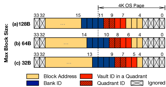

In a higher level of abstraction, a 4 KB OS page is allocated in two banks across all vaults (HMC 1.1),666Note that two banks is when the max block size is set to 128 B. We can increase BLP in accessing a single page by reducing the max block size (Figure 3). promoting memory level parallelism for reading/writing the contents of a page. When we access multiple pages allocated serially in the physical address space, as the number of concurrent accesses to these pages increases, bank-level parallelism (BLP) increases as well. For instance, in a 4 GB HMC 1.1 with 16 banks per vault, because a single page occupies two banks in a vault, up to eight allocated pages reside in a vault. Therefore, for 16 vaults, the total number of pages we can access while increasing BLP is . In fact, combined with BLP that each page utilizes, the low-order-interleaved address mapping enables maximum BLP for sequential page accesses. To conclude, 3D DRAM exemplified by HMC presents new address space abstractions and associated performance implications, the understanding of which is necessary for optimizing compilers and data layout algorithms for maximizing performance potential. In a scenario that an application randomly accesses multiple pages, the frequency, size, and coverage (in terms of number of banks, vaults, and rows) of accesses determine performance. In this paper, we explore HMC design space to understand its full-scale impact on applications.
III Experimental Setup
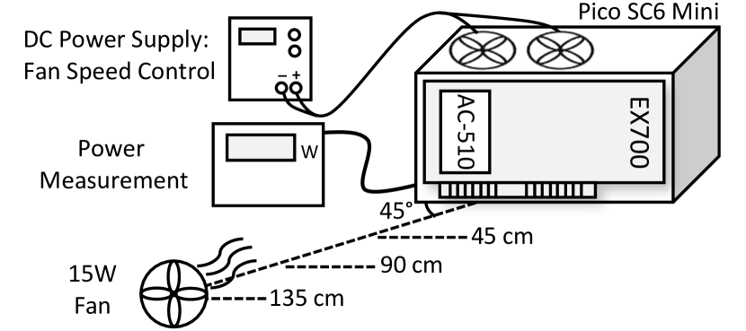
This section introduces the infrastructure, cooling equipment, and firmware, all of which are shown in Figure 4.
III-A Infrastructure Overview
Hardware: Our infrastructure, Pico SC-6 Mini [20], contains an EX700 [21] backplane, a PCIe 3.0 x16 board with 32 GB/s bandwidth. EX700 integrates a PCIe switch that routes host communication to up to six AC-510 [16] accelerator modules via PCIe 3.0 x8 buses. Each module has a Kintex UltraScale Xilinx FPGA777Part#: xcku060-ffva1156-2-e connected to a 4 GB HMC Gen2 (the same as Figure 2) with two half-width (8 lanes) links operating at 15 Gbps, so the bi-directional peak bandwidth is 60 GB/s, as Equation 2.
Thermal Measurements: To cool both the FPGA and HMC, an active heatsink equivalent to a low-end active cooling solution with $30 cost [12] is attached on top of the accelerator module. Figure 5a and 5b display the accelerator module with and without the heatsink, respectively. For thermal evaluations, we run each experiment for 200 seconds,888For all experiments, after 200 seconds, temperature is stable. and we measure the heatsink surface temperature of HMC using a thermal camera (Flir One [22]). Since thermal resistance of a transistor chip is smaller than that of the external heatsink, temperature of the heatsink surface is 5–10 degrees Celsius lower than that of the in-package junction [23]. The FPGA and HMC share the heatsink, but HMC is distinguishable in thermal images, and it has a higher temperature than its surroundings do, as seen in the thermal images of HMC at two temperatures in Figure 5c and 5d.
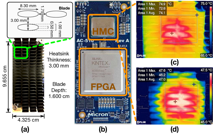
In other words, the shared heatsink does not prevent us from observing the effect of temperature variation because (\romannum1) HMC creates a heat island, which indicates it causes temperature increments, (\romannum2) FPGA performs the same tasks during experiments, so its heat dissipation is constant, and (\romannum3) in real systems, one component in the box is always affected by the heat profile of other components. In near-processor architectures, the temperature of an HMC is always affected by the temperature of a computational component such as a GPU, a CPU, or an FPGA. The thermal coupling between the FPGA and HMC is a factor of the integration substrate. Our measurements represent the PCB coupling, a much weaker coupling than integration of compute and memory in interposer or 3D. Thus, the configuration of our experiments is a realistic representation of a future design.
| Configuration | DC Power Supply: | 15 W Fan | Average HMC | |
|---|---|---|---|---|
| Name | Voltage | Current | Distance | Idle Temperature |
| Cfg1 | 12 V | 0.36 A | 45 cm | C |
| Cfg2 | 10 V | 0.29 A | 90 cm | C |
| Cfg3 | 6.5 V | 0.14 A | 90 cm | C |
| Cfg4 | 6.0 V | 0.13 A | 135 cm | C |
Cooling Environment: The PCIe backplane resides in a case and is air cooled via two fans attached to the top of the case111111These fans are for cooling only the backplane and not the machine. (total measured power of 4.5 W with 12 V). To mimic the thermal impact of PIM techniques, which is a potential application for 3D-stacked memories, we create various thermal environments (see Table II) by tuning the speed of the fans with a DC power supply, and placing a commodity fan (Vornado Flippi V8) with a measured power of 15 W and at an angle of at three distances (45, 90, and 135 cm). Figure 4(a) shows a diagram of our cooling environment.
Power Measurements: During the experiments, with a power analyzer, we monitor the power consumption of the machine, which includes the power of the FPGA, HMC, and PCIe switch on the backplane, and report the average of the power usage. Cooling fans are connected to another power source. Since during experiments the host and FPGA do not communicate, the power consumption of the PCIe switch is negligible. Thus, power consumption above the idle power of the machine, 100 W, is counted towards the activity of the HMC and the FPGA. In our infrastructure, we cannot decouple the power consumption of these two components since they share the same board and power supply. However, since the FPGA performs same task in all the experiments, variation in measured power is attributed to the HMC.
III-B Firmware and Software Overview
We use various firmware (i.e., digital design on the FPGA) and software combinations to perform experiments. To measure the properties of accesses to the HMC with various address patterns, we use the Pico API [24] and a Verilog implementation of GUPS, which measures how frequently we can generate requests to access memory locations (Figure 4(b)). The FPGA uses Micron’s controller [25] to generate packets for the multi-port AXI-4 interface between the FPGA and HMC. The Pico API initializes the hardware and provides an environment with the host OS to communicate with the FPGA on each accelerator module. Although the Pico API provides an interface to access HMC through the FPGA, since its read and write operations are bundled with software, a pure software solution to measure the bandwidth lacks sufficient speed. Therefore, to generate and send various mixes of requests, we use GUPS, which utilizes the full potential of available HMC bandwidth. As the frequency of the FPGA is low (187.5 MHz), to saturate the available bandwidth, GUPS uses nine copies of the same module, or ports to generate requests. Each port includes a configurable address generator, a monitoring unit to measure read latencies, a read tag pool with the depth of 64, and an arbitration unit to generate the type of a request (read or write). Each port is configurable to send read only (ro), write only (wo), or read-modify-write (rw) requests for random, or linear mode of addressing. Furthermore, requests can be mapped to a specific part of the HMC by forcing some bits of the address to zero/one by using address mask/anti-mask registers. We use the following three implementations:
Full-scale GUPS: To measure bandwidth, temperature, and high-load latency of various access patterns, we use full-scale GUPS, which utilizes all nine ports. For such experiments, first, we activate the ports, set the type of requests and size, their mask and anti-mask, and linear or random addressing mode. Then, we read the total number of accesses, maximum/minimum of read latency, and aggregate read latency after 20 seconds for bandwidth and 200 seconds for thermal measurements. We calculate bandwidth by multiplying the number of accesses by the cumulative size of request and response packets including header, tail and data payload (shown in Table I), and dividing it by the elapsed time. Experiments are done with full-scale GUPS, unless stated otherwise.
Small-scale GUPS: To measure latency-bandwidth relationships, we use a variation of full-scale GUPS, small-scale GUPS, in which we change the number of active ports to tune the request bandwidth. Similar to full-scale GUPS, we perform each experiment for 20 seconds.
Stream GUPS: We use Xilinx’s AXI-Stream interface to send/receive a group of requests/responses through streams to each port. Stream interface provides fast and efficient communication between the host and the FPGA. With stream GUPS, we also confirm the data integrity of our writes and reads. To measure low-load latency, we use stream GUPS, so that we can tune the number of requests.
IV Experimental Results
IV-A Address Mapping Experiments
To characterize the bandwidth properties of HMC, we explore a range of address space mappings to its abstraction hierarchy (i.e., quadrants, vaults, and banks) by generating random accesses throughout the address space and evaluating the achieved bandwidth. Address space mappings are achieved by starting with the default low-order interleaved address space mapping with 128 B blocks (as described in Section II-C) and then applying an eight-bit mask, which forces eight bits of address to 0. By applying the mask to various bit positions we map the address space across quadrants, vaults and banks. Figure 6 shows measured bandwidth for three request types of ro, wo, and rw with the size of 128 B.
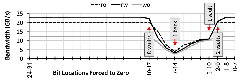
In this figure, bandwidth is the lowest when the mask is applied to bits 7-14, which forces all references to bank 0 of vault 0 in quadrant 0 (Figure 3a). The bandwidth rises with masking higher bits after the lowest bandwidth point because we incrementally spread the requests over more vaults, quadrants, and banks with the masks after that. Bandwidth experiences a large drop from masking bits 2-9 to the masking bits 3-10 in ro and rw because for the latter mask the accesses are restricted to a single vault with maximum internal bandwidth of 10 GB/s [26]. In the rest of the paper, based on the results of this section, we create targeted access patterns. For instance, a 2-bank access pattern targets two banks within a vault, and a 4-vault access pattern targets all the banks within four vaults.
IV-B Bandwidth Experiments
Figure 7 illustrates the bandwidth of various access patterns. As we pointed out in Section IV-A, since the bandwidth of a vault is limited to 10 GB/s, we observe that accessing more than eight banks of a vault does not affect the bandwidth for all types of accesses. For distributed accesses, in which addresses are spread across the address space (e.g., across vaults and banks), bandwidth of rw is higher than that of ro because as read-modify-write operations consists of a read followed by a write, both its request and response include data payloads, so rw utilizes bi-directional links more effectively. Meanwhile, as reads and writes are not independent, the number of reads are limited by the number of writes. Therefore, the bandwidth of rw is roughly double the bandwidth of wo.
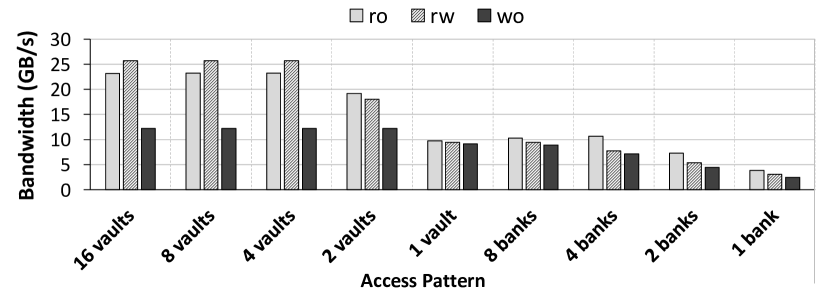
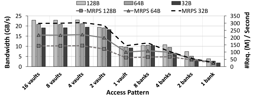
Figure 8 depicts the bandwidth of ro with the request sizes of 128, 64, and 32 B. As discussed in Section II-C, the granularity of the DRAM data bus within a vault is 32 B, and DRAM row size is 256 B. Therefore, reading the values smaller than 32 B requires one data transfer, and reading values larger than 32 B requires multiple data transfers. Note that since the maximum request size is smaller than the DRAM row size and HMC follows the closed-page policy, each request incurs the cost of opening just one DRAM row. (We investigate the effects of closed-page policy in Section IV-D.) Figure 8 also presents million requests per second (MRPS) for each data size. Although for less distributed access patterns (e.g., two banks) we see a similar number of requests, for distributed access patterns (e.g., 4, 8, and 16 vaults), the MRPS differs in various request sizes. For instance, when accesses distributed over 16 vaults, for small request sizes such as 32 B, HMC handles twice as many requests as large request sizes such as 128 B. This behavior in the number of requests handled by HMC, combined with the relatively same bandwidth utilization for various request sizes, demonstrates that the bottleneck in bandwidth is limited by DRAM timings and communication bandwidth, rather than the size of components in the FPGA such as GUPS buffers, tag-pool, or in internal memory controllers within vaults. In addition to request sizes shown in Figure 8, we perform the same experiments with all possible request sizes121212Possible request sizes are: 16, 32, 48, 64, 80, 96, 112, and 128 B. Note that for each request, we have an overhead of 16 B as well. Therefore, as size increases, the efficiency of data size to overhead also increases. and discover that the trend in both bandwidth and MRPS is similar.
IV-C Thermal and Power Experiments
In general, 3D systems present limiting thermal and power challenges. Therefore, we are interested in understanding the relationships between temperature, bandwidth, and power consumption particularly considering that the high speed links are responsible for significant power consumption. We are specially interested in the perspective of future PIM architectures that will create higher temperatures. Therefore, we push operation to the thermal limits by creating high-temperature environments through manipulation of the cooling configurations in Table II to study the relationship between temperature and bandwidth. We use synthetic address generation to explore these limits, and follow the methodology presented in Section III-B for temperature and power experiments. Figure 9 shows the outcomes of thermal experiments for cooling configurations shown in Table II. (This figure does not include configurations that trigger HMC failures.) Although experiments are limited by the resolution of the experimental infrastructure (°C), the absolute temperature values provide a close approximation for temperature-related behaviors.
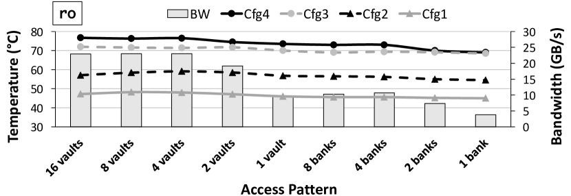
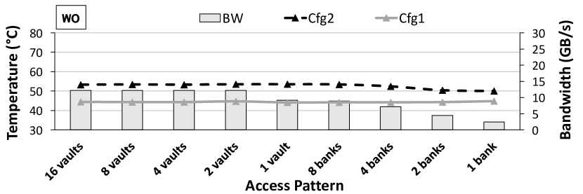
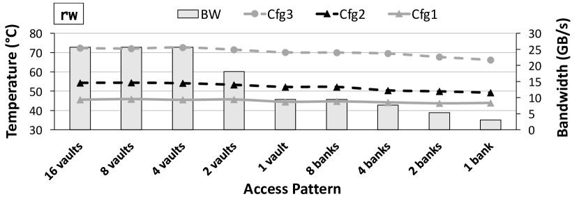
The first observation is that the behavior of HMC temperature (i.e., the reduction of temperature when bandwidth decreases) is similar in all cooling environments. That is, during the first three access patterns (accessing 16 to four vaults), in which bandwidth utilizations are similar, temperature remains constant. Then, during the execution of the rest of the access patterns (accessing two vaults to one bank), in which the bandwidth utilization decreases, temperature drops. In fact, more bandwidth utilization causes more accesses in DRAM layers, processes in memory controller, and data transfers in SerDes circuits, which consume 43% of total power [4, 3, 5]. As bandwidth utilization increases, HMC temperature rises, which directly affects the power consumption. Note that the bandwidth profile is directly affected by access patterns. Since HMC, a 3D-stacked design, has a smaller size than traditional DRAM DIMMs and has the capability to achieve high bandwidth (by exploiting serial communication and high BLP), we conclude that HMC and generally 3D-stacked memories are susceptible to thermal bottleneck.
As mentioned, previous work assumed that the reliable temperature bound of DRAM is °C [12, 13]. To distinguish the operational temperature for HMC, we run several experiments, forcing higher thermal fields by controlling the cooling configurations during which failures occur around the same temperatures. Operationally, to indicate an inevitable thermal failure (i.e., shutdown), HMC uses the head/tail of response messages to transmit this information to the host. Occurrence of a thermal failure during an experiment stops the HMC and recovery from it entails following steps: Cooling down, resetting HMC, resetting FPGA modules such as transceivers, and initializing HMC and FPGA. Notice that when failure occurs, stored data in DRAM is lost. Data recovery must rely on external techniques such as checkpointing and rollback. During our experiments, we observe that read-only accesses do not experience any thermal failures, even with the lowest cooling environment in Cfg1, in which temperature reaches to °C. However, for wo and rw requests, the same cooling environment (Cfg1) triggers thermal failures. Hence, our experiments indicate that reliable temperature bound is lower for workloads with significant write content - around °C, which is about °C lower than that for read-intensive accesses.
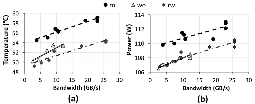
The relationship between the bandwidth and temperature, shown conceptually in Figure 1a, is drawn in Figure 11a with a linear regression fit to measured data. Figure 11 is extracted based on results in Cfg2, a configuration with highest temperature, in which none of the ro, wo, or rw experienced any thermally induced failures, providing a fair comparison. As this graph illustrates, when bandwidth increases from five to 20 GB/s, the temperature rises °C and °C for ro and rw accesses respectively. The positive slope of all three lines in the graph illustrates that the temperature bottleneck with increasing bandwidth is inevitable in such 3D memory organizations and therefore this characterization is important. Also, the greater slope of the line corresponding to wo indicates that write operations are more temperature sensitive across this bandwidth range. We could not assert the reason behind this with our current infrastructure. However, the results suggest that such sensitivity favors read-intensive workloads such as streaming applications to maximize bandwidth capacity.
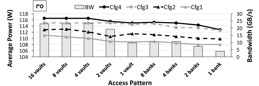
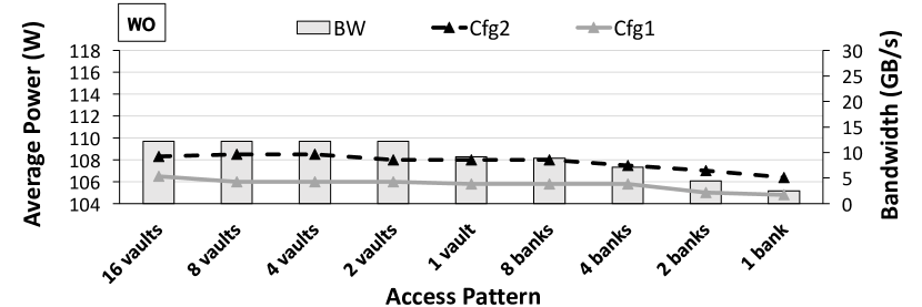
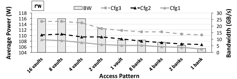
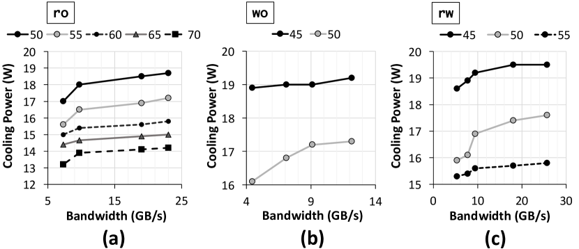
Figure 10 illustrates power consumption behavior across request types and distributions. First, as one might expect power consumption increases with increased bandwidth. Second, decreased cooling capacity leads to higher power consumption for the same bandwidth reflecting the coupling between power and temperature. This is particularly important to be aware of for PIM configurations. Figure 11b provides a linear regression fit line based on data from Figure 10. The figure illustrates a 2 W increment in device power consumption when bandwidth utilization rises from five to 20 GB/s. However, cooling capacity is also another contributing factor to power consumption. In fact, the cooling solution that is required to maintain a device at a reliable temperature, can consume significant power, and we study the impact as follows. With respect to voltage and current, listed in Table II for two PCIe backplane fans, and by the fact that as distance increases, the effective power consumption for cooling of the external fan decreases, we calculated the power consumption of each cooling configurations as 19.32, 15.9, 13.9, and 10.78 W for Cfg1 to Cfg4, respectively. Then, by using linear regression over measured data of temperature and bandwidth (Figure 9), we extract the graphs in Figure 12, which reflect the conceptual behaviors shown in Figure 1b. In Figure 12, each line shows required cooling power for maintaining a specific temperature as bandwidth utilization increases. Note that the absolute values of cooling power are related to our cooling infrastructure. However, Figure 11b and 12 indicate that as bandwidth utilization increases, power consumption of both the device and the cooling solution increases. In average, an increase of 16 GB/s in bandwidth causes a growth of 1.5 W in cooling power. Also, as the peak temperature increases exponentially with the proximity of the compute unit [12], adding PIM-like capabilities in the logic layer significantly increases the cost of cooling.
IV-D Closed-Page Policy Experiments

As discussed in Section II-C, the HMC implements a closed-page policy. While with the open-page policy, the average latency of linear accesses is lower than that of random accesses because of row buffer hits; with a closed-page policy, the average latencies of linear and random accesses should be the same. To illustrate this, we perform an experiment by issuing linear and random addresses and measure the bandwidth utilization. As Figure 13 illustrates, the bandwidth of random and linear accesses are similar (random accesses, compared to linear accesses, have slightly higher bandwidth because of fewer conflicts on any of the shared resources). We conjecture that the increase in bandwidth from 32 B blocks to 128 B blocks is due to efficiencies in streaming a block size greater than the width of the 32 B DRAM bus and reduced packet overhead due to the larger data size. We observe that applications benefit from increasing parallelism over vaults and banks (e.g., stripe data across the vaults and banks), rather than increasing reference locality. For instance, a streaming application that exhibits linear references should not allocate data sequentially within a vault for two reasons: (\romannum1) The maximum internal bandwidth of a vault is 10 GB/s, which limits the total bandwidth; and (\romannum2) references to successive addresses cannot exploit spatial locality because of the closed-page policy. Furthermore, to increase the effective bandwidth, the application should use 128 B size for requests because each request/response has an overhead of one flit, so a larger data size utilizes the available bandwidth more effectively. For instance, when using 128 B request size, the effective bandwidth is of raw bandwidth. However, when using 16 B request size, the effective bandwidth is of raw bandwidth. Therefore, the OS, memory controller, or programmer has to promote parallelism, remapping of data, and concatenation of requests to achieve high effective bandwidth.
IV-E Latency Experiments
As HMC, a 3D-stacked design, exploits packet-switched interfaces for scalability and PIM features, it yields another important performance attribute, latency, a less-focused attribute in traditional DIMM memories because of their constant timing characteristics. Thus, we dedicate this section to latency experiments and deconstruction of its contributing factors.
1) Contributing factors: Each port in the GUPS (Section III-B) measures the read latency as the number of cycles from when a read request is submitted to the HMC controller (on the FPGA) until the port receives the read response. This latency includes cycles for (1) arbitrating among ports, (2) creating a packet (i.e., generating head and tail flits, converting to flits, adding sequence numbers, and generating CRCs), (3) performing flow control, (4) converting the packet to the SerDes protocol [15], (5) serializing the packet, (6) transmitting the packet on the links, (7) processing the packet in the HMC (or memory) and generating a response, (8) transmitting the response back, (9) deserializing the response, (10) performing necessary verifications (i.e., checking errors and sequence numbers), and (11) routing the response back. Although conventional memory access latency for DDR memories is only reported by including items 6 to 8, a comprehensive latency should also include the number of cycles of similar related items.131313The reason for that items from 6 to 8 are reported in the JEDEC is that the standard specifies deterministic latencies, and the memory controller is on the host side. Therefore, memory vendors are not responsible for extra latencies. In addition, since packet communication enables features such as data integrity, remaining items might have noticeable latencies, so reporting only the items from 6 to 8 does not faithfully represent latency.
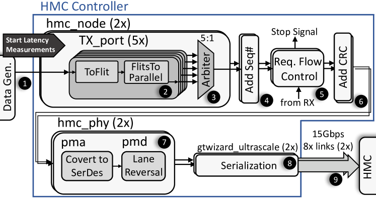
To understand the factors which contribute to latency, we inspect the latencies associated with each module in the transmit (TX) and receive (RX) paths by time stamping requests and reading the stamps from each module. Figure 14 presents the latency deconstruction of the TX path after a request is submitted to the HMC controller. Each external link is connected to an hmc_node module, which consists of five TX_ports that correspond to a port. Since the AC-510 has two links to the HMC, this means 10 ports are available on the FPGA, but one is reserved for system use. After a request is submitted to the HMC controller (❶ in Figure 14), the TX_port unit converts it to flits and buffers up to five flits in the FlitsToParallel unit (❷), which takes ten cycles or 53.3 ns (based on the max frequency of the FPGA at 187.5 MHz). Then, flits from each port are routed to subsequent units in a round-robin fashion by an arbiter (❸). This routing latency is between two to nine cycles. Afterwards, Add-Seq#, Req. Flow Control, and Add-CRC units contribute a latency of ten cycles (❹, ❺, and ❻, respectively). These units add fields in packets for reordering and data integrity. Moreover, if the number of outstanding requests exceeds a threshold, the request flow-control unit sends a stop signal to the corresponding port (❺) requesting a pause in the generation of memory access requests. For low-contention latency measurements, the request flow-control unit does not stop the transfer of any flit. Finally, flits are converted to the SerDes protocol [15] and serialized (❼ and ❽, respectively), which takes around ten cycles. In addition, transmitting one 128 B request takes around 15 cycles (❾). Overall, up to 54 cycles, or 287 ns, are spent on the TX path. Similarly, for a packet, 260 ns are spent on the RX path. In total, 547 ns of measured latency is related to link transfers and packet generation on the FPGA. Note that this is the minimum latency and is incurred when the flow-control unit does not stall transfers. For high-load studies, queuing delays will substantially increase this latency measurement.
2) Low-load latency: This paragraph explores the latency of low-load read accesses (i.e., no-load latency) and demonstrates the correlation between latency and the number of read accesses for varied packet sizes. As mentioned in Section III-B, for these explorations, we use stream GUPS. Each subfigure of Figure 15 shows variations in average, minimum, and maximum latency when the number of read requests in a stream changes from two to 28. This figure provides the following information about the behavior of low-load accesses.
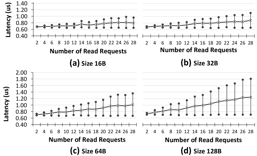
First, a comparison between the slopes of four diagrams in this figure reveals that when the request size is larger, latency increases faster with regard to the number of read requests. In other words, the latency of a stream of 28 large packets (i.e., 128 B packets) is 1.5x as high as that of a stream of 28 short packets (i.e., 16 B packets). However, a small stream (e.g., a stream of two packets) incurs almost the same latency regardless of packet size. Second, based on Figure 15, as we expected, the increase in average latency comes from increasing maximum latencies. This is probably primarily as a result of interference between packets in the logic layer which increases with number of references and size of packets. In addition, unlike maximum latencies, minimum latencies have a constant value as the number of requests increases. Third, the results for various sizes show that the minimum latency of 128 B packet sizes is 711 ns, 56 ns higher than that of 16 B packet sizes. We should also add delay for transition across the interface between a GUPS port and the HMC controller — not expected to be more than a few cycles in the low-load case. These latencies contain 547 ns infrastructure-related latency, so in average 125 ns is spent in the HMC. The latency variation within HMC is due to packet-switched interface, and TSV and DRAM timings. In comparison with typical DRAM access latency for a closed-page policy, we estimate the latency impact of a packet-switched interface to be about two times higher. In return, we obtain higher bandwidths via high BLP, more scalability via the interconnect, and better package-level fault tolerance via rerouting around failed packages.
3) High-load latency:
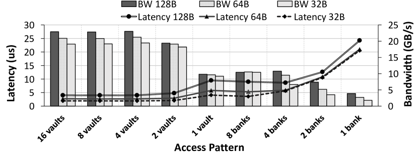
Figure 16 illustrates the latency behavior of high-load accesses (ro). The read latency varies from 1,966 ns for 32 B requests spread across 16 vaults to 24,233 ns for 128 B requests targeted to a single bank. The average reference latency of a high-load access pattern is 12 times as high as that of a low-load access pattern. These latency measurements are made at the data generation component of a GUPS port and prior to the HMC controller. At high loads, reference requests are queued up at the HMC controller input and we conjecture that the bulk of the growth in latency is due to this queuing delay. This observation is supported by the fact that the bandwidth utilization profile is similar across all experiments described earlier. Further, the latency of 32 B read requests is always lower than that of 64 B and 128 B read requests because the granularity of the DRAM data bus within each vault is 32 B, as pointed out in Section II-C. Therefore, the memory controller in the logic layer has to wait a few more cycles when accessing data larger than 32 B. Figure 16 shows that latency is directly related to bandwidth. A more distributed access pattern exploits both multiple vault controllers and BLP. By contrast, a targeted access pattern to a vault or to the banks within a vault incurs high latency because of the serialization of requests and limited number of resources per bank. The micro-second order of reported values for latency illustrates the importance of understanding the internal structure and abstractions supported by HMC, sensitivity to the internal frequency of operation,141414 As Lee et al. [27] pointed out, current 3D-stacked designs operate at lower frequencies than DDRs (e.g., Wide I/O [28] operates at 200-266 MHz while DDR3 operates at 2,133 MHz). and the importance of the design of the host-side memory interfaces.
4) Bandwidth-latency relationship: To explore bandwidth and latency relationship, we first examine two specific access patterns, and then all access patterns by using small-scale GUPS. As pointed out in Section III-B, we use small-scale GUPS to tune the request rate by changing the number of active ports. Figure 17a presents the results for read accesses to four banks within a vault. The figure, an actual demonstration of Figure 1c, shows that latency saturates at some rates that vary according to the packet size. This limiting factor that causes saturation can be the size of a queue in the vault controller. By assuming that a vault controller is a black box that includes a server and a queue, the average number of requests in a vault controller can be calculated based on Little’s law by multiplying the average time a request spends in the controller (i.e., vertical axis) by the input rate (i.e., horizontal axis) at the saturated point, the result of which provides the number of outstanding requests in terms of bytes. By accounting for the request sizes, we achieve a constant number, 375.
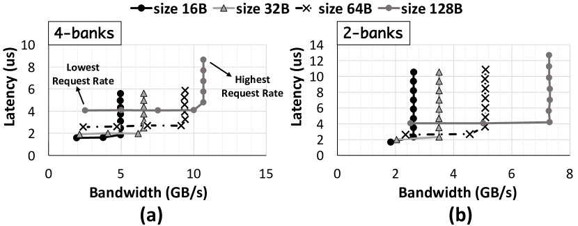
Similar analysis of Figure 17b infers that the number of outstanding requests for two-bank accesses is half of that for four-bank accesses. This observation suggests that a vault controller has one queue for each bank or for each DRAM layer.
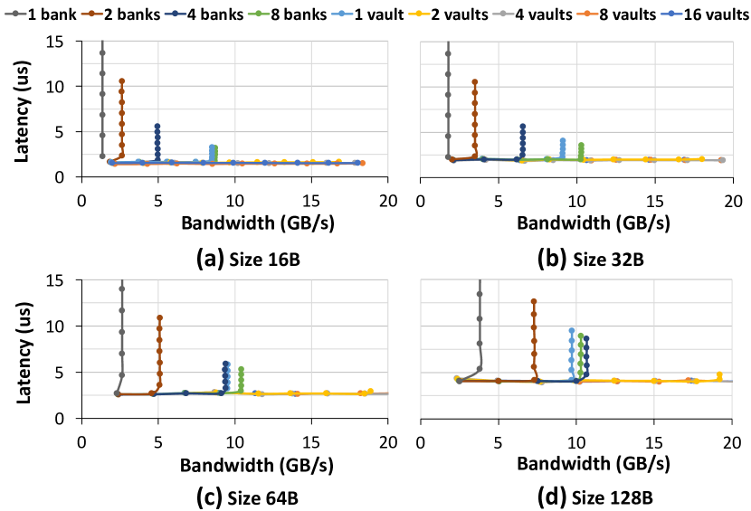
To explore further the limits of latency, Figure 18 presents an extended version of Figure 17 for various sizes and access patterns. As shown, accesses to more than eight banks of a vault do not follow the inferred trend of doubling the number of outstanding requests (i.e., benefiting from BLP) followed by accesses to one, two, and four banks. In fact, another factor, which is 10 GB/s access bandwidth within a vault, is responsible for this limitation. In addition, when accesses are spread over two vaults, the saturation point occurs at 19 GB/s, which is about 2x as high as that at 10 GB/s, the bandwidth limit of a vault. Notice that since we could not generate more parallel accesses to the HMC, the saturation points of accesses to more than two vaults does not occur. These results reiterate the importance of understanding the internal structure and abstractions of HMC for maximizing application performance. Besides, some limits exist on vault bandwidth (10 GB/s) that can be exceeded by appropriate data layout schemes. Further, we note the asymmetry in requests, for example each read request can consume 128 B of return bandwidth while the request itself takes only 16 B. Thus, achievable bidirectional bandwidth is derated from the peak bandwidth. Appropriate data mappings are necessary to not derate achievable bandwidth further.
V Related Work
HMC is a practical 3D-stacked memory that integrates DRAM dies and computational logic. Understanding the features of HMC is crucial for state-of-the-art applications that want to benefit from high bandwidth or low latency. Therefore, this work, in continuation of previous studies, have explored the characterization of HMC in terms of bandwidth, latency, thermal behavior, and power consumption. Recently, actual hardware-based studies continued the trend of HMC characterization, started by simulation-based explorations. In a technical report, Rosenfeld et al. [29] explored HMC performance in terms of bandwidth, latency and power consumption under HMCSim simulation. They showed that maximum link efficiency is achieved by a read ratio between 53% to 60% (based on packet size). The conclusion was while only memory-intensive applications achieve remarkable speedup from HMC, all applications may benefit from the low power consumption of HMC. In the first real-world HMC characterization work, Gokhale et al. [11] measured bandwidth and latency of HMC 1.1 by running a set of data-centric benchmark using an FGPA emulator. They showed that read-dominated applications achieve a 80% of peak bandwidth. Moreover, they discern that high concurrency of accesses leads to an exponential increase in latency. Furthermore, they reported a correlation between latency and bandwidth, in which latency changes from 80 ns for serial workloads, to 130 ns for concurrent workloads, while the bandwidth increases from 1 GB/s to 65 GB/s and power consumption increases from 11 W to 20 W.
In another real-world characterization study, Schmidt et al. [9] characterized HMC 1.0 using OpenHMC, an open-source digital design (i.e., infrastructure). They confirmed previously mentioned simulation-based results that a read ratio between 53% to 66% maximizes the access bandwidth of HMC. Moreover, they showed that read latency increases dramatically to more than 4000 ns, if the read ratio exceeds the optimal rate. However, for less than 53% read ratio, a total read latency of 192 ns and 224 ns (for 12.5 and 10 Gpbs respectively) is reported. Also, the power consumption, measured in that paper is up to 9 W. In another experimental paper, Ibrahim et al. [10] analyzed the effect of spatial and temporal locality of accesses to HMC on its throughput with an EX800 backplane consisting of four Stratix FPGAs. They emphasized that access patterns with high temporal and spatial locality can operate up to 20 times as fast as other applications. Similar to our result, their outcome reveals that write bandwidth is lower than read bandwidth. While these studies, including our work, agree on the general performance behaviors in terms of bandwidth and latency, as a result of varied platforms, some of the provided results are slightly different. Although previous work have illustrated fascinating facts about the features of HMC, these real-world characterization studies have not covered the impact of utilizing desirable features of HMC on temperature, power consumption, and latency.
In the meantime, some of the recent studies explored thermal behavior of HMC by simulation. Zhu et al. [12] analyzed the thermal behavior of PIM systems, in which processing elements are integrated with die-stacked memory. They show that a higher ambient temperature lowers the power budget for each functional unit at PIM. Also, to provide a safe operational environment for PIM, a stronger cooling solution (i.e. costlier in terms of price and power consumption) should be used. In addition, Eckert et al. [13] evaluated various cooling solutions for PIM-based systems. Their simulation using HotSpot showed that a low-cost passive heatsink is enough for keeping DRAM under the threshold temperature (C), while provisioning sufficient power for computations in memory. While simulation-based thermal analysis in these works yields useful insights, it does not accurately reflect the actual issues and the correlation between bandwidth, temperature, and power consumption.
VI Conclusion
This work demystified the characteristics of HMC, one of the two commodity 3D-DRAM technologies, which represents a class of 3D memories with high internal concurrency. The insights and projected results are generic not only to the class of 3D-memory systems but also to architectures that utilize packet-switched communications. Our experiments revealed the following key insights: (\romannum1) To efficiently utilize bi-directional bandwidth, accesses should have large sizes and use a mix of reads and writes. (\romannum2) To avoid structural bottlenecks and to exploit BLP, accesses should be distributed and request rate should be controlled from any level of abstraction (i.e., OS, compiler, software, or hardware). (\romannum3) To avoid complexity, one should not consider to improve performance resulting from spatial locality. (\romannum4) To benefit from scalability of packet-switched communications, a low-latency infrastructure is crucial. (\romannum5) To enable temperature-sensitive operations, fault-tolerant mechanisms should be employed. (\romannum6) To attain high bandwidth, optimized low-power mechanisms should be integrated with proper cooling solutions. While some experiments in this papers provide anticipated results, they yield a concrete real measured data to verify and also to explore future architecture research for an emerging technology.
Acknowledgments
We thank anonymous reviewers for their valuable comments and feedbacks for improving the paper. Our experimental hardware is partially supported by Micron. This study was supported in part by National Science Foundation under grant number CCF-1533767.
References
- [1] JEDEC Solid State Technology Association and others, “JEDEC Standard: DDR4 SDRAM,” JESD79-4, Sep, 2012.
- [2] D. U. Lee et al., “25.2 A 1.2V 8Gb 8-channel 128GB/s High-Bandwidth Memory (HBM) Stacked DRAM with Effective Microbump I/O Test Methods Using 29nm Process and TSV,” in ISSCC’14, pp. 432–433.
- [3] J. Jeddeloh and B. Keeth, “Hybrid Memory Cube New DRAM Architecture Increases Density and Performance,” in VLSIT’12, pp. 87–88.
- [4] S. Pugsley et al., “NDC: Analyzing the Impact of 3D-Stacked Memory+Logic Devices on MapReduce Workloads,” in ISPASS’14, pp. 190–200.
- [5] L. Nai et al., “GraphPIM: Enabling Instruction-Level PIM Offloading in Graph Computing Frameworks,” in HPCA’17, pp. 457–468.
- [6] D. Zhang et al., “TOP-PIM: Throughput-Oriented Programmable Processing in Memory,” in HPDC’14, pp. 85–98.
- [7] G. Kim et al., “Memory-Centric System Interconnect Design with Hybrid Memory Cubes,” in PACT’13, pp. 145–156.
- [8] K. Hsieh et al., “Transparent Offloading and Mapping (TOM): Enabling Programmer-Transparent Near-data Processing in GPU Systems,” in ISCA’16, pp. 204–216.
- [9] J. Schmidt et al., “Exploring Time and Energy for Complex Accesses to a Hybrid Memory Cube,” in MEMSYS’16, pp. 142–150.
- [10] K. Z. Ibrahim et al., “Characterizing the Performance of Hybrid Memory Cube Using ApexMAP Application Probes,” in MEMSYS’16, pp. 429–436.
- [11] M. Gokhale et al., “Hybrid Memory Cube Performance Characterization on Data-Centric Workloads,” in IA3’15, pp. 7:1–7:8.
- [12] Y. Zhu et al., “Integrated Thermal Analysis for Processing In Die-Stacking Memory,” in MEMSYS’16, pp. 402–414.
- [13] Y. Eckert et al., “Thermal Feasibility of Die-Stacked Processing in Memory,” in WoNDP’14.
- [14] J. Macri, “AMD’s Next Generation GPU and High Bandwidth Memory Architecture: FURY,” in HCS’15, pp. 1–26.
- [15] HMC Consortium, “Hybrid Memory Cube Specification 1.1,” Retrieved from hybridmemorycube.org, [Online; accessed 6/1/17].
- [16] PicoComputing, “AC-510 HPC Module,” http://picocomputing.com/ac-510-superprocessor-module/, [Online; accessed 6/1/17].
- [17] HMC Consortium, “Hybrid Memory Cube Specification 2.0,” Retrieved from hybridmemorycube.org, [Online; accessed 6/1/17].
- [18] HMC Consortium, “Hybrid Memory Cube Specification 1.0,” Retrieved from hybridmemorycube.org, [Online; accessed 6/1/17].
- [19] T. Pawlowski, “Hybrid Memory Cube (HMC),” in HCS’11, pp. 1–24.
- [20] PicoComputing, “SC6-Mini,” http://picocomputing.com/products/picocube/picomini/, [Online; accessed 6/1/17].
- [21] PicoComputing, “EX700 Backplane,” http://picocomputing.com/products/backplanes/ex-700/, [Online; accessed 6/1/17].
- [22] FLIR, “FLIR One Thermal Camera,” http://www.flir.com/flirone/ios-android/, [Online; accessed 6/1/17].
- [23] E. Bogatin et al., Roadmaps of Packaging Technology. Integrated Circuit Engineering, 1997.
- [24] PicoComputing, “Pico Framework Documentation,” http://picocomputing.zendesk.com/hc/, [Online; accessed 6/1/17].
- [25] PicoComputing, “HMC Controller IP,” [Online; accessed 6/1/17].
- [26] Rosenfeld, Paul, “Performance Exploration of the Hybrid Memory Cube,” Ph.D. dissertation, University of Maryland, College Park, 2014.
- [27] D. Lee et al., “Simultaneous Multi-Layer Access: Improving 3D-Stacked Memory Bandwidth at Low Cost,” TACO, vol. 12, no. 4, pp. 63:1–63:29, 2016.
- [28] J.-S. Kim et al., “A 1.2 V 12.8 GB/s 2 Gb Mobile Wide-I/O DRAM With 4 x 128 I/Os Using TSV Based Stacking,” Journal of Solid-State Circuits, vol. 47, no. 1, pp. 107–116, 2012.
- [29] P. Rosenfeld et al., “Peering Over the Memory Wall: Design Space and Performance Analysis of the Hybrid Memory Cube,” Technical Report UMD-SCA-2012-10-01, University of Maryland, Tech. Rep.