Passivation of dangling bonds on hydrogenated Si(100)-21: a possible method for error correction in hydrogen lithography
Abstract
Using combined low temperature scanning tunneling microscopy (STM) and atomic force microscopy (AFM), we demonstrate hydrogen passivation of individual, selected dangling bonds (DBs) on a hydrogen-passivated Si(100)-21 surface (H–Si) by atom manipulation. This method allows erasing of DBs and thus provides an error-correction scheme for hydrogen lithography. Si-terminated tips (Si tips) for hydrogen desorption and H-terminated tips (H tips) for hydrogen passivation are both created by deliberate contact to the H–Si surface and are assigned by their characteristic contrast in AFM. DB passivation is achieved by transferring the H atom that is at the apex of an H tip to the DB, reestablishing a locally defect-free H–Si surface.
pacs:
61.43.-j,68.35.Dv,68.37.Ef,68.37.Ps,71.55.Ak,72.20.Jv,81.65.RvI Introduction
Hydrogen lithography Lyding et al. (1994); Shen et al. (1995), that is controlled dehydrogenation of H-passivated semiconductor surfaces has become an important tool in the development of novel atomic scale logic devices and for the study of nanoscale and quantum physics. To this end, individual H atoms are deliberately desorbed from an H-passivated surface using a scanning probe microscopy tip by applying a voltage between tip and sample. An individual DB is created where a H atom is removed. Such DBs can be employed directly to construct atomically precise DB structures or they can be used for further processing. Importantly, DBs provide adsorption sites for single molecules, e. g. phosphine, which after incorporation and activation provides individual phosphorous dopants Schofield et al. (2003); Ruess et al. (2004). In addition, individual organic molecules can be captured and studied at individual DBs Hersam, Guisinger, and Lyding (2000); Piva et al. (2005); Godlewski et al. (2013).
Several proposals for novel, disruptive technologies are based on hydrogen lithography with atomic precision. These proposals include silicon-based solid state quantum computers Simmons et al. (2003), field-coupled silicon atomic quantum dots Wolkow et al. (2014), quantum Hamiltonian boolean logic gates Kolmer et al. (2015). Single atom transistors Fuechsle et al. (2012) and atomic-scale wires Weber et al. (2012) fabricated by hydrogen lithography followed by phosphor doping have already been demonstrated. Moreover, DBs provide an interesting model system for studying quantum physics, e. g. artificial molecules can be created and studied Schofield et al. (2013); Wood et al. (2016). Importantly, the DBs can adopt different charge states, depending on the global doping concentration and precise location of nearby charges, providing possible electrostatic coupling and switching schemes Haider et al. (2009); Labidi et al. (2015). In addition, the position of a DB can be switched within a dimer Bellec et al. (2013); Engelund et al. (2016), molecules can be adsorbed at DBs Hersam, Guisinger, and Lyding (2000); Piva et al. (2005), and their orientation can be changed by atomic manipulation Godlewski et al. (2016) representing mechanical atomic switches.
For complex devices, single DBs have to be placed with atomic precision with a high yield. The yield has been extensively studied and continuously been improved over the last two decades Shen et al. (1995); Stokbro et al. (1998); Soukiassian et al. (2003); Randall et al. (2009); Ballard et al. (2013); Kolmer et al. (2014); Wolkow et al. (2014); Møller et al. (2017), now reaching a yield of 0.8 to 0.9 (Ref. Wolkow et al., 2014). However, for complex, atomically precise structures needed for the envisioned applications an almost perfect yield is desired. Here, we demonstrate error correction for hydrogen lithography. We describe and demonstrate a method that can be used to cure, i. e., passivate individual selected DBs at will, recovering locally a defect-free hydrogen passivated surface. The method is fully compatible with hydrogen lithography. Therefore, faulty written DB structures can be erased and rewritten until all errors are removed yielding atomically precise DB structures.
To the best of our knowledge, erasing single DBs selectively by hydrogenation has not been shown before. Reversible passivation of silicon dangling bonds was demonstrated using a radical organic molecule adsorbed at the DB Pitters et al. (2003). Hydride formation by atomic manipulation was to date only reported on bare, non-passivated Si surfaces and only from molecular hydrogen (H2) by applying voltage pulses Kuramochi, Uchida, and Aono (1994); Kuramochi, Uchida, and Kuwahara (1997); Labidi, Kantorovich, and Riedel (2012).
The key for the correction of DB structures is the control of the tip functionalization. It has been shown before that the final tip atom is of utmost importance for AFM imaging with atomic resolution Gross et al. (2009); Sharp et al. (2012); Yurtsever et al. (2013); Sweetman et al. (2016); Labidi et al. (2017) and the importance of the tip for hydrogen lithography has been pointed out Møller et al. (2017). On hydrogenated Si surfaces two distinctly different tip functionalizations have been achieved, characterized and assigned using the combination of STM and AFM Sharp et al. (2012); Yurtsever et al. (2013); Sweetman et al. (2016); Labidi et al. (2017). On the one hand a chemically inert tip was assigned as an H tip Sharp et al. (2012); Labidi et al. (2017), and on the other hand a highly reactive tip was assigned as a Si tip Sweetman et al. (2016), the latter enabling even room-temperature atomic-resolution imaging of organic molecules by AFM Iwata et al. (2015). We achieved writing and correcting Si DBs by employing these two different tip functionalizations: a Si tip is used to write DBs, that is for hydrogen desorption, and a H tip is used for error correction, that is for hydrogen passivation. In the latter case the H from the tip apex is transferred into the DB, removing the defect, resulting in an H-terminated Si surface that cannot be distinguished from the pristine H–Si surface and at the same time the tip is changed from an H to a Si tip.
II Experimental details
We used a Si(100) wafer with high n-type doping (phosphor dopant concentration of , room temperature resistivity of ). To prepare the sample in UHV (base pressure ) the wafer was flash-annealed to several times to remove the native oxide. During the final anneal the chamber pressure remained below . Subsequently, the sample was H-passivated for using a hydrogen atom beam source at a partial H2 pressure of , with the sample held at a temperature of . Then, the sample was transferred to the STM/AFM stage.
All experiments were carried out at a temperature of using a qPlus sensor Giessibl (1998) (eigenfrequency , stiffness , quality factor ) operated in frequency-modulation modeAlbrecht et al. (1991). The oscillation amplitude was set to . The bias voltage was applied to the sample. The PtIr tip of the sensor had previously been cut by focused ion beam and then, in UHV at low temperature, indented into a Cu(111) sample to obtain an atomically sharp, metallic, Cu covered tip.
STM (AFM) images were recorded in constant-current (constant-height) mode and show the topography (frequency shift ). All filled (empty) state STM images shown here were acquired at () with the tunneling current set to . AFM images were recorded at . The height offset, (), is given for each AFM image with respect to the STM set point for filled (empty) state imaging above the bare H–Si surface. Both Si and H tips were created by bringing the tip into contact with the H–Si surface at . The tips were assigned by their AFM contrast as explained in the following.
III Results
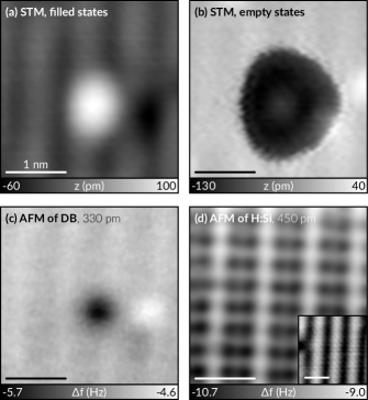
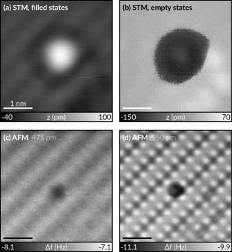
STM and AFM images with the different tip functionalizations are shown in Fig. 1 for the reactive Si tip and in Fig. 2 for the inert H tip, respectively. Our results are in agreement with previous studies Livadaru et al. (2011); Yurtsever et al. (2013); Taucer et al. (2014); Rashidi et al. (2016); Sharp et al. (2012); Sweetman et al. (2016); Labidi et al. (2017). For STM images we observed a qualitatively similar contrast for both tips and the tips cannot unambiguously be assigned by STM images. At filled state imaging with both tips [Fig. 1(a) and Fig. 2(a)] the dimer rows appear as faint protrusions and the DB appears as a protrusion with an lateral extension of about and an apparent height of about . At empty state imaging [Fig. 1(b) and Fig. 2(b)] the DB appears as a dark disc (depression) of about lateral extensions and an apparent depth of about with a faint protrusion in the center. Recently, the STM contrast could be successfully explained in detail by Refs. Livadaru et al., 2011; Taucer et al., 2014; Rashidi et al., 2016. Importantly, the charge state of the DB is affected during imaging by both tip-induced band bending (TIBB) and, in the opposite way, by dynamic charging through electron attachment/detachment by tunneling from/onto the tip. Therefore, the contrast crucially depends on the applied voltage, the lateral and vertical tip location, and the doping of the substrate. Sharp transitions in the STM images indicate a change of the DB charge state as a function of lateral tip position, e. g. observed at the rim of the dark disc in Fig. 1(b) and Fig. 2(b).
We obtained constant-height AFM images with both tips at different tip heights . To achieve atomic resolution in AFM, the tip is approached considerably compared to STM imaging. First, we discuss the frequency shift contrast of a Si tip. Fig. 1(c) shows an AFM image of the same area as Figs. 1(a,b) at with the dimer rows appearing slightly darker (more negative ) than the background, and the DB appearing as a dark circular feature. Typically, approaching a Si tip closer to a DB results in tip changes and local destruction of the surface, presumably due to bond formation between tip and sample. Therefore, to illustrate the atomic contrast of Si tips, Fig. 1(d) shows an AFM image of a defect-free area with the same Si tip at . The hydrogenated Si atoms appear as dark circular features revealing the reconstruction.
Next, we discuss the frequency shift contrast with a H tip. Figs. 2(c) and 2(d) show AFM images of the same area as Figs. 2(a,b) at and , respectively. As in the case of Si tips described in the previous section, the dimer rows appear slightly darker than the background in Fig. 2(c), and the DB appears as the darkest feature. Importantly, in contrast to the Si tip, the hydrogenated Si atoms appear as bright circular features with the H tip at closer approach [Fig. 2(d)] in agreement with Ref. Labidi et al., 2017. Dark corresponds to a decreased (more negative) frequency shift and, as we work in the attractive regime, i. e., on the rising branch of (where a larger corresponds to a larger tip-sample distance), this corresponds to increased attractive forces. As described in Refs. Sharp et al., 2012; Sweetman et al., 2016 the Si tip yields an increase in attractive forces above hydrogenated Si sites while the passivated H tip yields a slightly reduced attraction above hydrogenated Si sites compared to the average H–Si surface.
The DB itself is imaged dark with both tips [Fig. 1(c) and Fig. 2(c,d)]. The contrast can be tentatively explained by attractive electrostatic interaction due to a negatively charged DB. Note that the contrast changes for differently charged DBs. However, a detailed investigation of the charge state of the DB within the band gap, based on Kelvin probe force microscopy, goes beyond the scope of this paper.
We used Si tips to write DBs. Typically, a voltage of at tunneling currents on the order of was used to create an individual DB within less than . We did not optimize the writing of DBs in our work, which had been investigated systematically before Ballard et al. (2013); Kolmer et al. (2014); Møller et al. (2017); Wolkow et al. (2014).
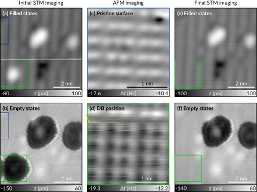
In the following, the controlled specific hydrogenation of a DB is demonstrated in Fig. 3. First, we imaged an area with several DBs using STM with a H tip, see Fig. 3(a,b). The H functionalization of the tip is confirmed by its characteristic AFM contrast (hydrogenated Si sites appear bright) on a DB-free area, as presented in Fig. 3(c). A zoom-in on the DB in the region indicated by the green square is shown in Fig. 3(d). During that AFM image [Fig. 3(d)], which was recorded at a tip height closer to the surface as compared to Fig. 2(d), the contrast suddenly changed from that of a H tip (hydrogenated Si sites bright) to the typical contrast of a Si tip (hydrogenated Si sites dark). After that AFM image no trace of the DB could be observed in subsequent STM images [Fig. 3(e,f)] signaling that the DB was removed. We can conclude that the H atom of the H tip apex was transferred to the DB during the AFM image in Fig. 3(d). In contrast to the hydrogen desorption process (DB creation) no voltage or tunnel current was applied for the DB hydrogenation.
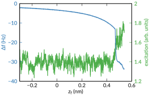
H passivation of DB was achieved routinely when a H tip was used. The H was transferred from the tip to the DB during imaging. Passivation could also be achieved by vertical manipulation, i. e. approaching a H tip vertically towards a DB as demonstrated in Fig. 4. In that case, DB passivation is signalled by a sudden change in frequency shift (to more negative values) and a correlating increase in the excitation signal of the sensor. In general, the requirement for DB passivation was a tip approach closer to the surface than necessary for typical AFM imaging. When the DB got passivated, the H tip was converted into a Si tip.
IV Conclusion
We demonstrated that an individual, deliberately chosen DB defect on a H–Si surface can be hydrogen-passivated to reestablish a locally defect-free surface. Passivation is achieved by atomic manipulation, transferring the H atom of a hydrogen-terminated tip into the DB. This method provides a proof of concept for error correction for hydrogen lithography and thus could significantly increase the yield for atomic precise structures written by hydrogen lithography. While AFM is very useful for the assignment of the tips, the correction method could also be established by STM only.
Acknowledgements.
We thank A. Fuhrer for discussions and help with the preparation of clean Si surfaces, and Rolf Allenspach for valuable comments on the manuscript. The research leading to these results received funding from the ERC Advanced Grant CEMAS (agreement no. 291194), the ERC Consolidator Grant AMSEL (682144), and the EU project PAMS (610446).References
- Lyding et al. (1994) J. W. Lyding, T. C. Shen, J. S. Hubacek, J. R. Tucker, and G. C. Abeln, Appl. Phys. Lett. 64, 2010 (1994).
- Shen et al. (1995) T. C. Shen, C. Wang, G. C. Abeln, J. R. Tucker, J. W. Lyding, P. Avouris, and R. E. Walkup, Science 268, 1590 (1995).
- Schofield et al. (2003) S. R. Schofield, N. J. Curson, M. Y. Simmons, F. J. Rueß, T. Hallam, L. Oberbeck, and R. G. Clark, Phys. Rev. Lett. 91, 136104 (2003).
- Ruess et al. (2004) F. J. Ruess, L. Oberbeck, M. Y. Simmons, K. E. J. Goh, A. R. Hamilton, T. Hallam, S. R. Schofield, N. J. Curson, and R. G. Clark, Nano Lett. 4, 1969 (2004).
- Hersam, Guisinger, and Lyding (2000) M. C. Hersam, N. P. Guisinger, and J. W. Lyding, Nanotechnology 11, 70 (2000).
- Piva et al. (2005) P. G. Piva, G. A. DiLabio, J. L. Pitters, J. Zikovsky, M. Rezeq, S. Dogel, W. A. Hofer, and R. A. Wolkow, Nature 435, 658 (2005).
- Godlewski et al. (2013) S. Godlewski, M. Kolmer, H. Kawai, B. Such, R. Zuzak, M. Saeys, P. de Mendoza, A. M. Echavarren, C. Joachim, and M. Szymonski, ACS Nano 7, 10105 (2013).
- Simmons et al. (2003) M. Y. Simmons, S. R. Schofield, J. L. O’Brien, N. J. Curson, L. Oberbeck, T. Hallam, and R. G. Clark, Surface Science 532-535, 1209 (2003).
- Wolkow et al. (2014) R. A. Wolkow, L. Livadaru, J. L. Pitters, M. Taucer, P. Piva, M. Salomons, M. Cloutier, and B. V. C. Martins, in Field-Coupled Nanocomputing (Springer Berlin Heidelberg, Berlin, Heidelberg, 2014) pp. 33–58.
- Kolmer et al. (2015) M. Kolmer, R. Zuzak, G. Dridi, S. Godlewski, C. Joachim, and M. Szymonski, Nanoscale 7, 12325 (2015).
- Fuechsle et al. (2012) M. Fuechsle, J. A. Miwa, S. Mahapatra, H. Ryu, S. Lee, O. Warschkow, L. C. L. Hollenberg, G. Klimeck, and M. Y. Simmons, Nature Nanotech. 7, 242 (2012).
- Weber et al. (2012) B. Weber, S. Mahapatra, H. Ryu, S. Lee, A. Fuhrer, T. C. G. Reusch, D. L. Thompson, W. C. T. Lee, G. Klimeck, L. C. L. Hollenberg, and M. Y. Simmons, Science 335, 64 (2012).
- Schofield et al. (2013) S. R. Schofield, P. Studer, C. F. Hirjibehedin, N. J. Curson, G. Aeppli, and D. R. Bowler, Nature Comm. 4, 1649 (2013).
- Wood et al. (2016) J. A. Wood, M. A. Rashidi, M. Koleini, J. L. Pitters, and R. A. Wolkow, (2016), 1607.06050 [cond-mat.mes-hall] .
- Haider et al. (2009) M. B. Haider, J. L. Pitters, G. A. DiLabio, L. Livadaru, J. Y. Mutus, and R. A. Wolkow, Phys. Rev. Lett. 102, 046805 (2009).
- Labidi et al. (2015) H. Labidi, M. Taucer, M. A. Rashidi, M. Koleini, L. Livadaru, J. L. Pitters, M. Cloutier, M. Salomons, and R. A. Wolkow, New J. Phys. 17, 073023 (2015).
- Bellec et al. (2013) A. Bellec, L. Chaput, G. Dujardin, D. Riedel, L. Stauffer, and P. Sonnet, Phys. Rev. B 88, 241406 (2013).
- Engelund et al. (2016) M. Engelund, S. Godlewski, M. Kolmer, R. Zuzak, B. Such, T. Frederiksen, M. Szymonski, and D. Sánchez-Portal, Phys. Chem. Chem. Phys. 18, 19309 (2016).
- Godlewski et al. (2016) S. Godlewski, H. Kawai, M. Kolmer, R. Zuzak, A. M. Echavarren, C. Joachim, M. Szymonski, and M. Saeys, ACS Nano 10, 8499 (2016).
- Stokbro et al. (1998) K. Stokbro, C. Thirstrup, M. Sakurai, U. Quaade, B. Y.-K. Hu, F. Perez-Murano, and F. Grey, Phys. Rev. Lett. 80, 2618 (1998).
- Soukiassian et al. (2003) L. Soukiassian, A. J. Mayne, M. Carbone, and G. Dujardin, Phys. Rev. B 68, 035303 (2003).
- Randall et al. (2009) J. N. Randall, J. W. Lyding, S. Schmucker, J. R. Von Ehr, J. Ballard, R. Saini, H. Xu, and Y. Ding, J. Vac. Sci. Technol. B 27, 2764 (2009).
- Ballard et al. (2013) J. B. Ballard, T. W. Sisson, J. H. G. Owen, W. R. Owen, E. Fuchs, J. Alexander, J. N. Randall, and J. R. Von Ehr, Journal of Vacuum Science & Technology B, Nanotechnology and Microelectronics: Materials, Processing, Measurement, and Phenomena 31, 06FC01 (2013).
- Kolmer et al. (2014) M. Kolmer, S. Godlewski, R. Zuzak, M. Wojtaszek, C. Rauer, A. Thuaire, J.-M. Hartmann, H. Moriceau, C. Joachim, and M. Szymonski, Applied Surface Science 288, 83 (2014).
- Møller et al. (2017) M. Møller, S. P. Jarvis, L. Guérinet, P. Sharp, R. Woolley, P. Rahe, and P. Moriarty, Nanotechnology 28, 075302 (2017).
- Pitters et al. (2003) J. L. Pitters, P. G. Piva, X. Tong, and R. A. Wolkow, Nano Lett. 3, 1431 (2003).
- Kuramochi, Uchida, and Aono (1994) H. Kuramochi, H. Uchida, and M. Aono, Phys. Rev. Lett. 72, 932 (1994).
- Kuramochi, Uchida, and Kuwahara (1997) H. Kuramochi, H. Uchida, and Y. Kuwahara, Jpn. J. Appl. Phys. 36, L1343 (1997).
- Labidi, Kantorovich, and Riedel (2012) H. Labidi, L. N. Kantorovich, and D. Riedel, Phys. Rev. B 86, 165441 (2012).
- Gross et al. (2009) L. Gross, F. Mohn, N. Moll, P. Liljeroth, and G. Meyer, Science 325, 1110 (2009).
- Sharp et al. (2012) P. Sharp, S. P. Jarvis, R. Woolley, A. M. Sweetman, L. N. Kantorovich, C. Pakes, and P. Moriarty, Appl. Phys. Lett. 100, 233120 (2012).
- Yurtsever et al. (2013) A. Yurtsever, Y. Sugimoto, H. Tanaka, M. Abe, S. Morita, M. Ondráček, P. Pou, R. Pérez, and P. Jelínek, Phys. Rev. B 87, 155403 (2013).
- Sweetman et al. (2016) A. M. Sweetman, J. Stirling, S. P. Jarvis, P. Rahe, and P. Moriarty, Phys. Rev. B 94, 115440 (2016).
- Labidi et al. (2017) H. Labidi, M. Koleini, T. Huff, M. Salomons, M. Cloutier, J. L. Pitters, and R. A. Wolkow, Nature Comm. 8, 14222 (2017).
- Iwata et al. (2015) K. Iwata, S. Yamazaki, P. Mutombo, P. Hapala, M. Ondráček, P. Jelínek, and Y. Sugimoto, Nature Comm. 6, 7766 (2015).
- Giessibl (1998) F. J. Giessibl, Appl. Phys. Lett. 73, 3956 (1998).
- Albrecht et al. (1991) T. R. Albrecht, P. Grütter, D. Horne, and D. Rugar, J. Appl. Phys. 69, 668 (1991).
- Livadaru et al. (2011) L. Livadaru, J. L. Pitters, M. Taucer, and R. A. Wolkow, Phys. Rev. B 84, 205416 (2011).
- Taucer et al. (2014) M. Taucer, L. Livadaru, P. G. Piva, R. Achal, H. Labidi, J. L. Pitters, and R. A. Wolkow, Phys. Rev. Lett. 112, 256801 (2014).
- Rashidi et al. (2016) M. Rashidi, M. Taucer, I. Ozfidan, E. Lloyd, and M. Koleini, Phys. Rev. Lett. 117, 276805 (2016).