————————–
Achiral tilted domain walls in perpendicularly magnetized nanowires
Abstract
Perpendicularly magnetized nanowires exhibit distinct domain wall types depending on the geometry. Wide wires contain Bloch walls, narrow wires Néel walls. Here, the transition region is investigated by direct imaging of the wall structure using high-resolution spin-polarized scanning electron microscopy. An achiral intermediate wall type is discovered that is unpredicted by established theoretical models. With the help of micromagnetic simulations, the formation of this novel wall type is explained.
In recent years, domain walls in perpendicularly magnetized materials have been intensely investigated because they are narrower than in in-plane systems and therefore, when used to store a data bit, promise higher storage density. In perpendicularly magnetized systems, domain walls are of Bloch type, i.e., the magnetization rotates within the wall plane. In in-plane magnetized systems, in contrast, diverse wall types exist. In bulk, again Bloch walls prevail, whereas in thin films, the energetically favored wall type is a Néel wall, i.e., the magnetization rotates perpendicularly to the plane of the wall. In between, a finite film-thickness range exists in which domain walls are neither of Bloch nor of Néel type. They are characterized by more complex arrangements of spins, such as zigzag patterns Shtrikman and Treves (1960), cross-ties Torok, Olson, and Oredson (1965) or continuous asymmetric deformations Rivkin et al. (2009). The Bloch wall is the energetically preferred state in perpendicularly magnetized films irrespective of film thickness. Néel walls can be made the ground state by changing the geometry to wires Martinez, Torres, and Lopez-Diaz (2011); DeJong and Livesey (2015) or adding constrictions Jubert and Allenspach (2005), by applying magnetic fields Miron et al. (2011); Ryu et al. (2013), or by introducing Dzyaloshinskii–Moriya exchange interaction (DMI) Thiaville et al. (2012).
The Bloch–Néel wall transition in perpendicularly magnetized nanowires, as a function of the wire width, was indirectly observed by measuring a change in the anisotropic magnetoresistance (AMR) Koyama et al. (2011). Most recently, it was studied analytically DeJong and Livesey (2015). A direct observation of this transition in real space is missing. Both Bloch and Néel walls were observed in thin films by spin-polarized scanning tunneling microscopy Meckler et al. (2009), in multilayers by spin-polarized low-energy electron microscopy Chen et al. (2013a), and in nanowires by optically monitoring the Zeeman shift of the electron spin in a nitrogen-vacancy defect in diamond Tetienne et al. (2015).
In this work, we investigate domain walls at the Bloch–Néel wall transition in flat nanowires (or “nanostrips”) with perpendicular magnetic anisotropy as a function of the nanowire width. We image the wall structure in real space using high-resolution spin-polarized scanning electron microscopy (spin-SEM), which is capable of determining the specimen’s magnetization by measuring the spin polarization of the low-energy secondary electrons emitted. We find Bloch domain walls in wide nanowires and Néel walls in narrow wires, and an intermediate domain wall type in between. This intermediate wall is characterized by a tilted magnetization direction pointing neither along the wire nor perpendicular to it. It marks the Bloch–Néel wall transition and has never been imaged before. We determine the domain wall profile and the azimuthal angle of the magnetization by fitting the profiles with a one-dimensional (1D) wall model. Micromagnetic simulations confirm this continuous transition via an intermediate domain wall and prove that this wall requires a nontrivial 2D arrangement of the spins.
The magnetic thin films Ta()/Pt()/ /Co()/Pt() were sputter deposited onto a Si/SiOx() substrate. Vibrating sample magnetometry was used to determine the saturation magnetization and the perpendicular anisotropy of the films. The nanowires were fabricated by Ar-ion milling through a 15-nm-thick Al mask that was patterned by electron-beam lithography and lift-off. The wires were shaped like a narrow bowtie, thus trapping the domain wall close to the center of the constriction upon application of an alternating perpendicular field to inject domain walls from adjacent large pads. Prior to magnetic imaging, the samples were sputtered with a ion beam of energy at normal incidence and a beam dose of in our ultra-high-vacuum system () to remove 1 nm of the Pt capping layer, thereby enhancing the spin polarization of the secondary electrons while still keeping the perpendicular anisotropy of the Co/Pt interface. The sputtering process is controlled by monitoring the atomic composition of the thin-film surface by Auger electron spectroscopy.
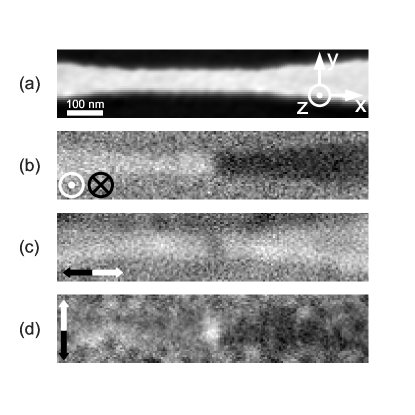
Magnetic nanowires of different widths were imaged in our spin-SEM Allenspach (2000). We present results from nanostrips with width between and , focusing mainly on a 70-nm-wide wire. The wire width was determined at the position of the domain wall directly from the scanning electron micrograph with an uncertainty of . The spin detector measures two components of the magnetization simultaneously. All three magnetization components were accessed by taking two consecutive images, the second one after rotating the sample by .
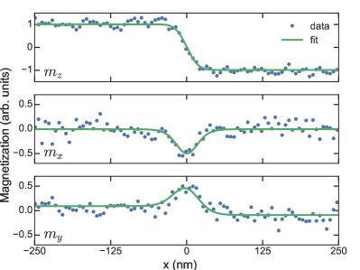
Figure 1 shows that the domain wall in the 70-nm-wide wire has magnetization components in both in-plane directions: It is neither a pure Bloch nor Néel wall, but intermediate between the two. A closer look reveals that the domain wall is inclined by with respect to the wire’s cross section. In Fig. 2 we plot the domain wall profiles () averaged along the y-direction across the wire. The wall profile in the 1D model is Jung et al. (2008):
| (1) | ||||
where is the domain wall width and is the center of the wall. The azimuthal angle is (or ) for a Néel wall and (or ) for a Bloch wall. In order to fit and , we take the finite resolution of the microscope into account, by assuming a Gaussian beam profile with a standard deviation of . Finally, by simultaneously fitting the profiles of the wall in the 70-nm-wide nanowire, we find and which is equivalent to . In the following, for convenience, we will display always as the smallest multiple. A small asymmetry in the measurement of the component is present, corresponding to a rotation of of the secondary electrons, which we attribute to a combination of misalignment of the sample normal with respect to the detector axes and spin rotation through the electron optics.
The results of several fitted walls are shown in Table 1.
| Nanowire width (nm) | (nm) | () |
|---|---|---|
| 57 | ||
| 70 | ||
| 93 | ||
| 300 |
We observe Bloch walls in nanowires of 93-nm width and above, a Néel wall in the 57-nm and an intermediate wall in the 70-nm-wide wire.
In the 1D wall model, the demagnetizing energy determines whether a Bloch or a Néel wall is the lowest energy state. Although surface and volume magnetic charges are arranged in a 2D fashion, overall the demagnetizing energy can be considered as a transverse anisotropy which depends on the nanowire dimensions Jung et al. (2008); Koyama et al. (2011). A consequence of the model is that the azimuthal angle changes discontinuously as a function of the nanowire width and thickness Jung et al. (2008); DeJong and Livesey (2015), contrary to our experimental findings. The possible existence of a “mixed wall” was discussed by Aharoni Aharoni (1966) in the context of in-plane magnetized films and discarded for the 1D case by a rigorous energy minimization of all possible configurations. However, he conjectured that wall types with 2D spin arrangements with lower energy might exist, explaining, for instance, the occurrence of cross-tie walls Torok, Olson, and Oredson (1965).
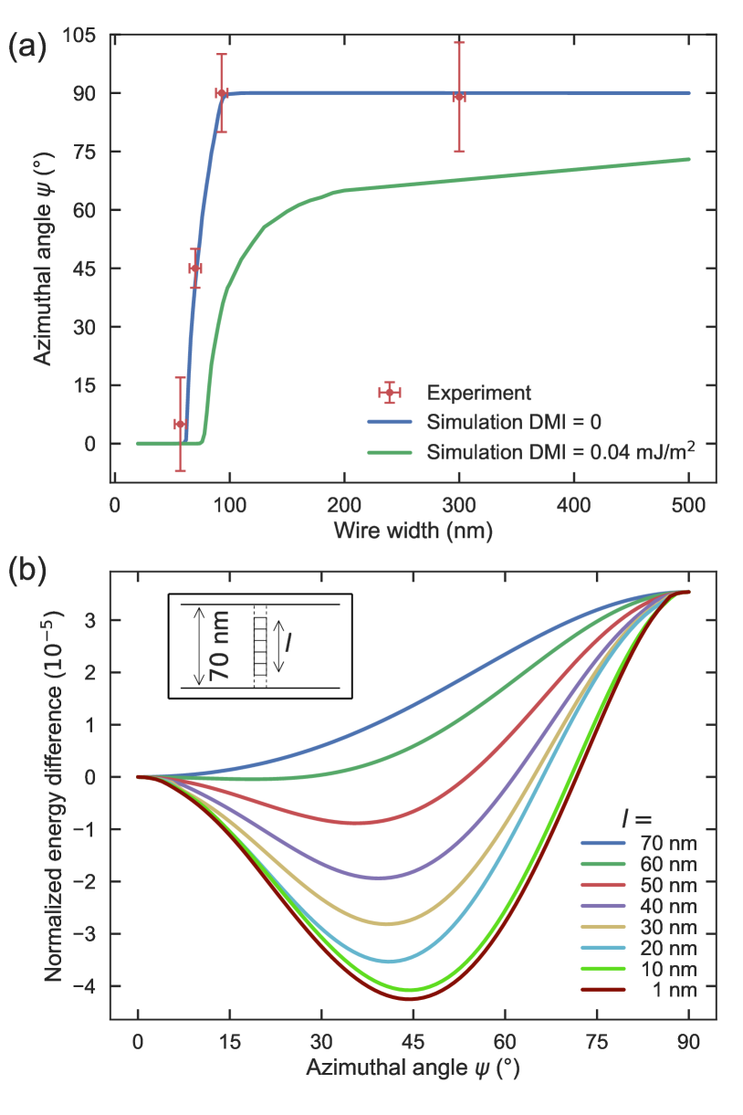
To overcome the limitations of the 1D model, we performed 2D micromagnetic simulations using OOMMF Donahue and Porter (1999). A wire with a length of 1200 nm and a width varying from 20 to 500 nm was modeled with a cell size of 1 nm 1 nm 3.8 nm. The material parameters used were , , and an exchange stiffness . For each simulation, the azimuthal angle was deduced from the relaxed energy state, see Fig. 3(a). As expected, we found Néel walls for narrow wires and Bloch walls for wide ones. The transition is not abrupt: changes continuously between and . The width at which this transition occurs depends on the values of the material parameters: For larger or larger the width gets larger, while for larger it gets smaller.
In order to scrutinize the discrepancy between the analytical model and micromagnetic simulations, a series of 2D simulations was run for a wire of 70-nm width. A line of spins within the wall was kept fixed (see inset in Fig. 3(b)), with their azimuthal angle varying from 0 to in increments of . The energy of the system is plotted in Fig. 3(b). For all spins fixed along the entire width, the lowest energy state is a Néel wall; no stable intermediate wall forms, despite the fact that the simulation is 2D. We then sequentially reduced the length of the line of fixed spins. In each series, starting from the edges, more spins were freed until in the extreme case only the spin in the center cell was kept fixed. A pronounced energy minimum develops at a non-trivial angle, i.e., an intermediate wall has formed. This proves that the intermediate wall is a consequence of the 2D nature of a domain wall in perpendicularly magnetized wires.
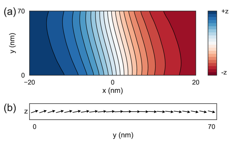
In this 2D wall, the spins tend to align parallel to the edges in order to lower magnetostatic energy, similar to the formation of a Néel cap at the surface of a bulk ferromagnet Scheinfein et al. (1989), and contrary to a tilted 1D wall. In a perpendicularly magnetized ferromagnet, uniaxial anisotropy energy can be gained by tilting the spins within the wall out of the plane. In in-plane magnetized materials, such a tilting generally occurs by forming a C- or S-shaped spin arrangement Guslienko et al. (2001), with a slight preference for the C-type because of the more complete flux closure of the stray field. Correspondingly, in our perpendicularly magnetized wire, a C-shaped arrangement is set up along the wire’s cross section, as shown in Fig. 4(b). Within the wire plane, a C-shape cannot evolve into the adjacent up/down magnetization in a continuous way, and hence an S-shape establishes itself, see Fig. 4(a), with an overall canting angle of the wall of . This inclination of the domain wall can also be seen in the measurements of Fig. 1(b)–(c). The contour levels in Fig. 4(a) reveal that the domain wall is slightly narrower at the edges than in the center, illustrating that spins tilt out-of-plane, which reduces the uniaxial anisotropy energy near the edges. Indeed, the overall energy gain of the intermediate wall compared with the Néel wall shown in Fig. 3(b) can be attributed to the anisotropy energy contribution. The azimuthal tilting of the spin within the wall is thus a consequence of the subtle interplay between anisotropy, exchange and demagnetizing energy. The first tilts the spins out of the plane, while the second keeps neighboring spins as aligned as possible. The third one balances the surface magnetic charges of the Bloch wall with the volume magnetic charges of a Néel wall. We suspect that an analogous situation exists in in-plane magnetized structures that are too small to support the wide extension of a cross-tie wall. Then the curved and tilted walls proposed long ago Shtrikman and Treves (1960) might form.
So far, we neglected another mechanism that can strongly influence the structure of the domain wall: The Dzyaloshinskii–Moriya exchange interaction Heide, Bihlmayer, and Blügel (2008); Thiaville et al. (2012); Chen et al. (2013a); Hrabec et al. (2014). Its strength is described by the constant , and its energy contribution per unit area for a Néel wall is depending on the chirality of the wall, and zero for the Bloch wall Thiaville et al. (2012). Strong DMI has been observed in asymmetric Co/Ni multilayers Chen et al. (2013b). It influences the Bloch–Néel transition by expanding the Néel wall regime towards wider and thicker nanowires, so that in films the preferred domain wall will be of Néel type or Bloch type with a strong Néel component, i.e., a chiral intermediate wall.
In our wires, however, DMI is not the cause of the intermediate domain wall. First of all, we find Bloch walls in extended square structures ( ) and in the film. Second, from Table 1, we see that in a 93-nm-wide nanowire and in a 300-nm-wide one. Within the experimental uncertainty, these walls can be considered as Bloch walls with vanishing (or very small) Néel component. A Néel component induced by DMI would be considerably more pronounced. To substantiate this, the micromagnetic simulations were repeated for wires with . The results are shown in Fig. 3(a). The striking difference is that deviates strongly from even at very large nanowire widths, for instance for a width of 500 nm. For the curve shown in Fig. 3(a), we have deliberately chosen a very small value of . The trend to favor a Néel wall component is even more pronounced for larger , which is reported in material stacks similar to ours Chen et al. (2013b). Therefore, we exclude that the intermediate walls we observe are caused by DMI.
An overall inclination of the wall, which in our intermediate wall is a direct consequence of the magnetization tilt, was observed in domain-wall motion experiments Yamanouchi et al. (2006); Ryu et al. (2012). It affects current-induced wall motion because of the induced wall pressure Viret et al. (2005). It was proposed that this inclination can be exploited to deduce the DMI value Boulle et al. (2013). With our finding of an intermediate wall, one needs to carefully examine in each case whether such an inclination is caused by DMI alone or whether an achiral intermediate wall – unrelated to DMI – contributes.
It is remarkable that this new wall type has been overlooked for so long. In wires in which both Bloch and Néel walls were identified Koyama et al. (2011), intermediate walls should show up with a distinct AMR, provided the equilibrium state is attained. In micromagnetic simulations, the intermediate wall is missed if the starting configuration is a Bloch or a Néel wall, as for instance in Ref. Martinez, Torres, and Lopez-Diaz (2011): The energy landscape is too flat there. Analytical approaches DeJong and Livesey (2015) captured the transition width accurately by developing sophisticated models for the magnetostatic energy, but were also unaware of the existence of a lower-energy 2D wall structure.
In conclusion, we determined the structure of domain walls as a function of the width of perpendicularly magnetized Co/Ni nanowires. Bloch walls prevail for wires wider than , Néel walls for wires narrower than . The transition is not abrupt, contrary to expectations based on the commonly considered 1D model: Intermediate walls form. We showed that such a transition does not require additional effective transverse fields nor DMI. The subtle balance of the various energy terms requires that the magnetization configuration adopts a 2D distribution across the wire. In particular, the spins within the wall tilt out of the plane when approaching the wire edge, in striking contrast to both a Bloch and a Néel wall. We argue that this intermediate wall type is a general phenomenon that should occur in any perpendicularly magnetized material provided the wire width is chosen appropriately. This width can be tuned by the perpendicular anisotropy, saturation magnetization, and exchange stiffness.
It would be interesting to investigate the consequences such continuous transition regions have on effects that rely on the discrete Bloch-to-Néel transition, such as the reported drastic reduction of the critical current in spin-transfer-driven domain wall motion Jung et al. (2008) or the deferral of the Walker breakdown to higher fields Martinez, Torres, and Lopez-Diaz (2011).
The authors are grateful to Karen L. Livesey for detailed insight into the one dimensional model and Gianfranco Durin and Simone Moretti for discussions. The research leading to these results has received funding from the European Union Seventh Framework Programme [FP7-People-2012-ITN] under grant agreements 316657 (SpinIcur) and 608031 (Wall).
References
- Shtrikman and Treves (1960) S. Shtrikman and D. Treves, J. Appl. Phys. 31, 1304 (1960).
- Torok, Olson, and Oredson (1965) E. J. Torok, A. L. Olson, and H. N. Oredson, J. Appl. Phys. 36, 1394 (1965).
- Rivkin et al. (2009) K. Rivkin, K. Romanov, Y. Adamov, A. Abanov, V. Pokrovsky, and W. M. Saslow, Europhys. Lett. 85, 57006 (2009).
- Martinez, Torres, and Lopez-Diaz (2011) E. Martinez, L. Torres, and L. Lopez-Diaz, Phys. Rev. B 83, 174444 (2011).
- DeJong and Livesey (2015) M. D. DeJong and K. L. Livesey, Phys. Rev. B 92, 214420 (2015).
- Jubert and Allenspach (2005) P.-O. Jubert and R. Allenspach, J. Magn. Magn. Mater. 290-291, 758 (2005).
- Miron et al. (2011) I. M. Miron, T. Moore, H. Szambolics, L. D. Buda-Prejbeanu, S. Auffret, B. Rodmacq, S. Pizzini, J. Vogel, M. Bonfim, A. Schuhl, and G. Gaudin, Nat. Mater. 10, 419 (2011).
- Ryu et al. (2013) K.-S. Ryu, L. Thomas, S.-H. Yang, and S. Parkin, Nat. Nanotech. 8, 527 (2013).
- Thiaville et al. (2012) A. Thiaville, S. Rohart, É. Jué, V. Cros, and A. Fert, Europhys. Lett. 100, 57002 (2012).
- Koyama et al. (2011) T. Koyama, D. Chiba, K. Ueda, K. Kondou, H. Tanigawa, S. Fukami, T. Suzuki, N. Ohshima, N. Ishiwata, Y. Nakatani, K. Kobayashi, and T. Ono, Nat. Mater. 10, 194 (2011).
- Meckler et al. (2009) S. Meckler, N. Mikuszeit, A. Preßler, E. Y. Vedmedenko, O. Pietzsch, and R. Wiesendanger, Phys. Rev. Lett. 103, 157201 (2009).
- Chen et al. (2013a) G. Chen, J. Zhu, A. Quesada, J. Li, A. T. N’Diaye, Y. Huo, T. P. Ma, Y. Chen, H. Y. Kwon, C. Won, Z. Q. Qiu, A. K. Schmid, and Y. Z. Wu, Phys. Rev. Lett. 110, 177204 (2013a).
- Tetienne et al. (2015) J.-P. Tetienne, T. Hingant, L. J. Martínez, S. Rohart, A. Thiaville, L. H. Diez, K. Garcia, J.-P. Adam, J.-V. Kim, J.-F. Roch, I. M. Miron, G. Gaudin, L. Vila, B. Ocker, D. Ravelosona, and V. Jacques, Nat. Commun. 6, 6733 (2015).
- Allenspach (2000) R. Allenspach, IBM J. Res. Develop. 44, 553 (2000).
- Jung et al. (2008) S.-W. Jung, W. Kim, T.-D. Lee, K.-J. Lee, and H.-W. Lee, Appl. Phys. Lett. 92, 202508 (2008).
- Aharoni (1966) A. Aharoni, J. Appl. Phys. 37, 3271 (1966).
- Donahue and Porter (1999) M. Donahue and D. Porter, Interagency Report NISTIR 6376. National Institute of Standards and Technology (1999).
- Scheinfein et al. (1989) M. R. Scheinfein, J. Unguris, R. J. Celotta, and D. T. Pierce, Phys. Rev. Lett. 63, 668 (1989).
- Guslienko et al. (2001) K. Y. Guslienko, V. Novosad, Y. Otani, H. Shima, and K. Fukamichi, Phys. Rev. B 65, 024414 (2001).
- Heide, Bihlmayer, and Blügel (2008) M. Heide, G. Bihlmayer, and S. Blügel, Phys. Rev. B 78, 140403(R) (2008).
- Hrabec et al. (2014) A. Hrabec, N. A. Porter, A. Wells, M. J. Benitez, G. Burnell, S. McVitie, D. McGrouther, T. A. Moore, and C. H. Marrows, Phys. Rev. B 90, 020402(R) (2014).
- Chen et al. (2013b) G. Chen, T. Ma, A. T. N’Diaye, H. Kwon, C. Won, Y. Wu, and A. K. Schmid, Nat. Commun. 4, 2671 (2013b).
- Yamanouchi et al. (2006) M. Yamanouchi, D. Chiba, F. Matsukura, T. Dietl, and H. Ohno, Phys. Rev. Lett. 96, 096601 (2006).
- Ryu et al. (2012) K.-S. Ryu, L. Thomas, S.-H. Yang, and S. S. P. Parkin, Appl. Phys. Express 5, 093006 (2012).
- Viret et al. (2005) M. Viret, A. Vanhaverbeke, F. Ott, and J.-F. Jacquinot, Phys. Rev. B 72, 140403(R) (2005).
- Boulle et al. (2013) O. Boulle, S. Rohart, L. D. Buda-Prejbeanu, É. Jué, I. M. Miron, S. Pizzini, J. Vogel, G. Gaudin, and A. Thiaville, Phys. Rev. Lett. 111, 217203 (2013).