Magnetic Field-Free Giant Magnetoresistance in
a Proximity- and
Gate-Induced Graphene Spin Valve
Abstract
Due to its two dimensional nature, ferromagnetism and charge doping can be induced by proximity and electric field effects in graphene. Taking advantage of these features, we propose an electrically engineered spin valve by combining two magnetic insulators (using EuO, EuS, or YIG) and three coating gates. Two top gates are used to cancel the heavy electron doping’s in these magnets and one back gate is used to utilize the normal or half-metallic ferromagnetisms. We demonstrate that, when the second top gate is tuned to utilize the insulating or spin insulating states, huge giant magnetoresistance (GMR) at high temperature (several times of at 68K and 100K) can be achieved for EuO and YIG. These results imply a distinguished GMR that is magnetism tunable, vertical configured (ferromagnetism versus insulating), and magnetic field-free. Our work may offer a viable path to a tantalizing magnetic field-free spintronics.
Graphene, although a diamagnetic material, is highly promising for spintronics. This is because it supports not only long diffusion lengths and long spin lifetimes at room temperature, but also magnetic moments induced by various methods Han et al. (2014). Introduction of vacancy defects, doping with molecules or elements with high spin-orbital coupling, and tailoring as zig-zag edged nanoribbons can induce ferromagnetism in graphene Han et al. (2014); Feng et al. (2017).
Among the proposed methods, graphene coupling with nearby magnetic insulators are the most intriguing way Feng et al. (2017). Theoretically, EuO, EuS, and yttrium iron garnet Y3Fe5O12 (YIG) have been predicted to induce ferromagnetism with heavy electron doping in graphene through proximity effect Haugen et al. (2008); Yang et al. (2013); Hallal et al. (2017). Nontrivial effects, such as simultaneous spin filter and spin valve effect Song and Dai (2015), pure crossed Andreev reflection Ang et al. (2016), and quantum anomalous Hall effect Su et al. (2017) have been proposed in graphene-EuO heterostructures. Experimentally, EuO has been integrated on graphene, in which ferromagnetism with 67K Curie temperature and heavy electron doping was confirmed Swartz et al. (2012, 2013). On the other hand, anomalous Hall effect Wang et al. (2015), spin-current convention Mendes et al. (2015), spin transport Leutenantsmeyer et al. (2016), and chiral charge pumping Evelt et al. (2017) have been demonstrated as a probe of the ferromagnetism in a graphene/YIG heterostructure. Similarly, Zeeman spin Hall effect Wei et al. (2016) was exhibited for that in a graphene/EuS heterostructure. These works reveal graphene on EuO, EuS, or YIG as emergency 2D ferromagnets.
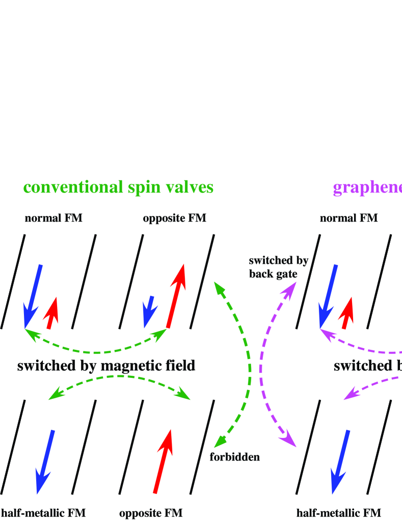
In this work, we explore giant magnetoresistance (GMR) applications of these ferromagnets. We propose a spin valve based on two magnetic insulators and three coating gates. Of them, two top gates are used to cancel the electron doping through the strong electric field effect Novoselov et al. (2004); Kim et al. (2012), and one back gate is used to utilize a normal or half-metallic ferromagnetism. We show that, when the second top gate is changed to make use of the insulating or spin insulating states, huge GMR at high temperature ( at 68 and 100K) can be achieved for EuO and YIG. These results imply a magnetic field-free (electrically engineered), vertical configured, and magnetism tunable GMR, which distinguishes remarkably from the conventional one (see Fig. 1). The proposed GMR offers not only a viable path to the tantalizing magnetic field-free spintronics, but also an evidence for the ferromagnetism. GMR based on graphene has been widely studied before Cheianov and Fal ko (2006); McCann et al. (2006); Haugen et al. (2008); Zhai and Chang (2008); Kim and Kim (2008); Muñoz-Rojas et al. (2009); Zhang et al. (2010); Lu et al. (2011); Bai et al. (2010); Friedman et al. (2010); Liao et al. (2012); Mendes et al. (2015); Gopinadhan et al. (2015); Kisslinger et al. (2015); Zhai and Wang (2016); Wu et al. (2017); El-Ahmar et al. (2017); however, the value is usually small and a magnetic field is indispensable.
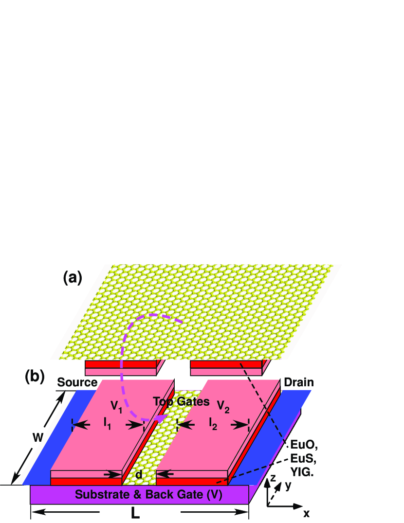
Figure 2 shows the proximity- and gate-induced spin valve. Two EuO(111), EuS(111), or YIG(111) substrates of lengths and and a distance are grown on top of two ‘top’ gates ( and ). On the substrates an Here graphene film is deposited Swartz et al. (2012); Wei et al. (2016); Wang et al. (2015). The whole structure is then turned over and transferred to a substrate contacting with a back gate (). The graphene is further contacted with source and drain electrodes (). As shown by first principle calculations Hallal et al. (2017), all the ferromagnets are heavily electron doped, which limits the spintronic application by a low polarization (about for EuO Yang et al. (2013)). Hole doping by magnetic insulator such as CFO was suggested to overcome this shortcoming Hallal et al. (2017). Here we propose a different way, i.e., by applying top gates. Through the strong electric field effect Novoselov et al. (2004); Kim et al. (2012), the Dirac points of the ferromagnets can be tuned to coincide with the pristine graphene’s.
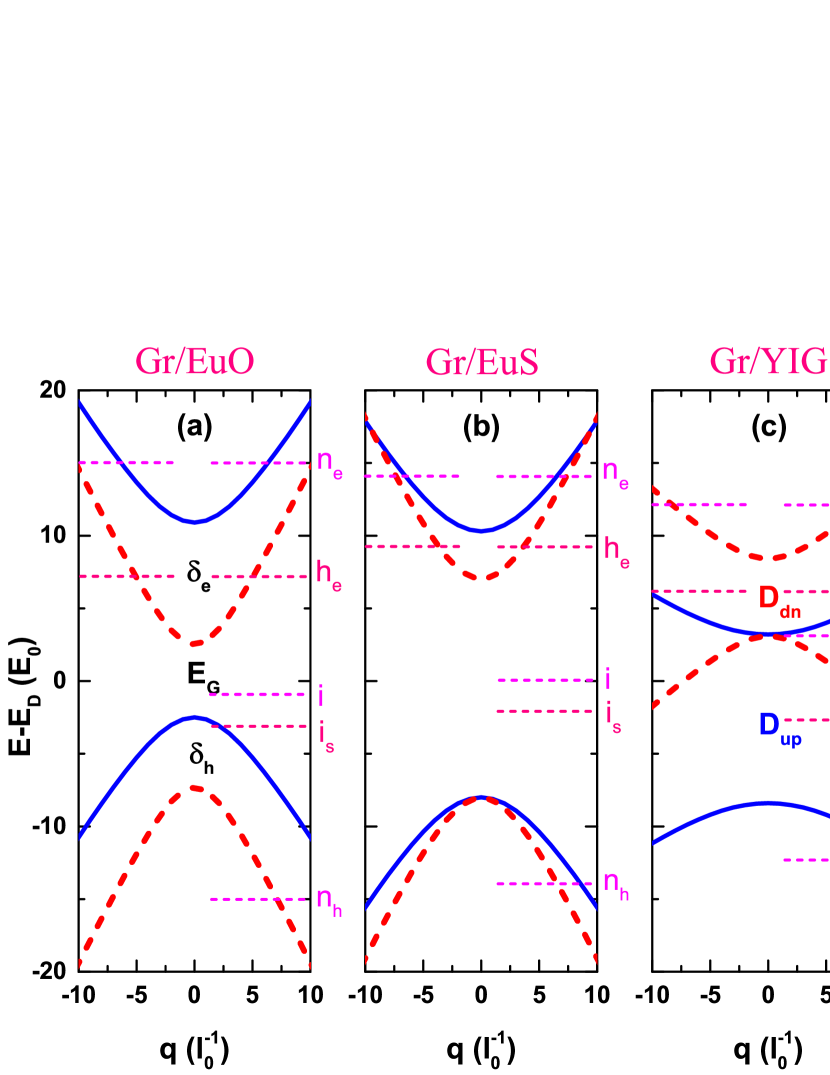
The Eu- (Fe-) states in the EuO and EuS (YIG) substrates are polarized. They overlap with the C- state in graphene and induce the ferromagnetism Yang et al. (2013); Hallal et al. (2017). The predicted energy dispersions of graphene on a six-bilayer EuO, EuS, and six-trilayer YIG substrates at the optimized distances Yang et al. (2013) are plotted in Fig. 3(a)-(c). Parabolic and spin resolved dispersions are clearly seen, from which normal and half-metallic ferromagnetisms for electron and hole (see lines labeled by and ), and insulating and spin insulating states ( and ) can be defined. For EuS the half-metallic ferromagnetism for hole is absent, while for YIG the insulating window is rather narrow. We have proposed to cancel the heavy electron dopings by top gates; here we propose to make use of the ferromagnetisms by the back gate. In the left magnet, both normal and half-metallic ferromagnetisms can be utilized by lifting the Fermi energy into corresponding windows. (Note this is rather hard for the conventional case.) We further propose that, by a top gate difference (), the electron ferromagnetisms in the right magnet can be switched to opposite (hole) ones, and even insulating and spin insulating states. These form the basis for the distinguished GMR.
Heavy electron doping’s (), band gaps opening at the Dirac points (), and exchange splittings ( and ) as labeled in Fig. 3(a) are observed as the ferromagnetisms. Accordingly, dispersions around the Dirac points were described by effective Hamiltonians in a sublattice-spin direct produce space Zollner et al. (2016); Su et al. (2017); Hallal et al. (2017). Note, in this space wave function should be solved as a four-components one even for a single valley Song and Wu (2013). The ferromagnetisms can also be defined by spin up and spin down () Dirac cone dopings (), Dirac gaps (), and Fermi velocities () as labeled in Fig. 3(c). These parameters relate with the above ones by and ; can be fitted from the original data (see Table 1 for parameters). In this view, the three magnets can be described by a uniform effective Hamiltonian in a simple sublattice space,
| (1) |
where is the momentum operator, is the pseudospin Pauli matrices, is the top gate voltages, is the identify matrix, and for valley and . For pristine and contacted graphene .
For brevity, we express all quantities in dimensionless form by means of a characteristic energy meV and corresponding length unit nm. The right- and left-going envelope functions () in the contacted, ferromagnetic, and pristine graphene () can be exactly resolved by decoupling . The result reads , where , , , , and with . From the continuity of envelope functions at the boundaries, transfer matrix can be constructed Song et al. (2012, 2013) and spin-resolved transmission coefficients can be obtained as Born and Wolf (1980). For 100K, the - and - inelastic scatterings can be ignored Morozov et al. (2008); Chen et al. (2008) and the ballistic spin-resolved conductance can be given by the Landauer-Büttiker formula Büttiker et al. (1985)
| (2) |
where is the Fermi-Dirac distribution function, and is the quantum conductance (2 accounts for the valley degeneracy). The zero-temperature conductance can be rewritten as where is half of the number of the transverse modes. The magnetoresistance (MR) is given by (in unit of ), and the GMR is defined by the ratio between the V and P configurations through .
| magnets | |||||||
|---|---|---|---|---|---|---|---|
| Gr/EuO | -132.8 | 13.4 | 1.337 | -139.4 | 9.8 | 1.628 | 69K |
| Gr/EuS | -128.85 | 18.3 | 1.40 | -130.5 | 15 | 1.60 | 16.5K |
| Gr/YIG | -80.6 | 11.6 | 0.63 | -83.75 | 5.3 | 0.70 | 550K |
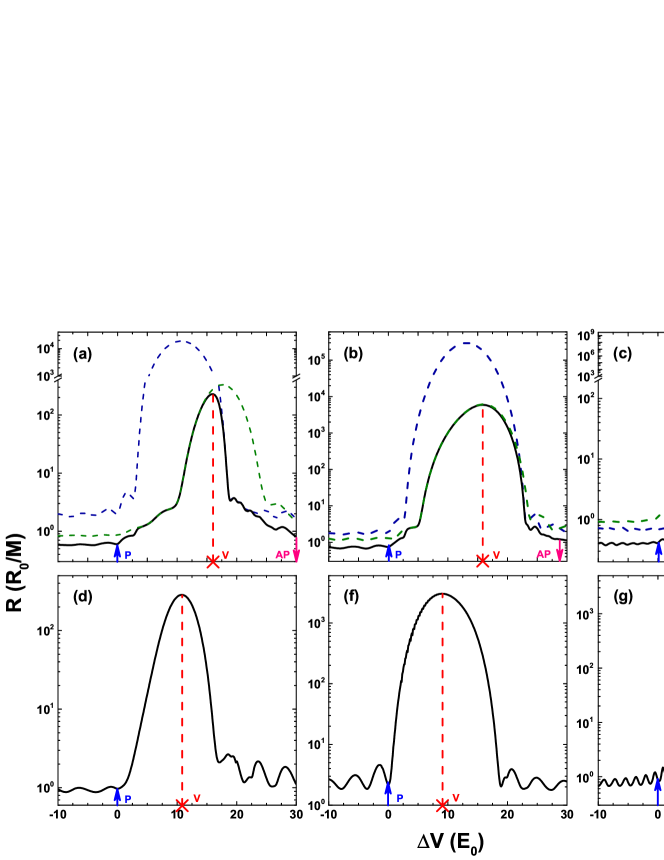
We first consider GMR utilizing the normal ferromagnetism. The MR and its spin components () as a function of the top gate difference are plotted in Fig. 4(a)-(c). As can be seen, the MR is rather low () when a same top gate () is applied on the right magnet (see the arrow labeled by P). This is the P configuration, for which both spins transport through the spin valve quasi-ballistically. When a gate difference is applied, the MR first increases and then decreases. Surprisingly, the maximal MR dose not happens at the AP configuration as the conventional case (see the arrow labeled by AP). Instead, it arises when the insulating state in the second magnet aligns to the Fermi energy (see the arrow labeled by V). This configuration falls in between the P and AP ones and can be defined as a vertical configuration. In the right magnets both spins are blocked for the V configuration, while transport quasi-ballistically again for the AP configuration. Comparing the MRs at these two configurations, we obtain a rather huge GMR with typical value of (see Table 2 for details). It is also seen that, the MR profile for YIG is rather sharp due to the rather narrow insulating window.
We then consider GMR utilizing the half-metallic ferromagnetism, for which only one spin contributes the MR. The MR profiles are plotted in Fig. 4 (d)-(g). It is not surprised that, rather low MR for the P configuration and rather high MR for the V configuration are observed again. Comparing them, a rather huge GMR with typical value of are obtained (see table 2). Interestingly, the high resistance for YIG shows rich resonant peaks. This is due to a much smaller Dirac gap for spin down, which supports much smaller resistance even for a blocked-blocked transport. It seems that, an AP configuration is responsible for the EuO and YIG cases. However, since spin up or spin down is always blocked, only the blocking of the initially transparent spin (spin down or up) is important. This is confirmed by the EuS case, where GMR happens in absence of opposite (hole) half-metallic ferromagnetism.
In conventional spin valves made of no matter normal Baibich et al. (1988) or half-metallic Hwang and Cheong (1997) ferromagnets, P and AP configurations are respectively responsible for the low and high MRs; they are switched by a magnetic field (see the left column in Fig. 1). The mechanism for the proximity- and gate-induced graphene spin valve is totally different. The V configuration is responsible for the high resistance states and it is switched from the P configuration by an electric field. Moreover, normal and half-metallic ferromagnetisms can also be switched by the back gate, which is usually forbidden for the conventional cases (see the right column in Fig. 1)
| ferromagnetisms () | |||
|---|---|---|---|
| 228.4/0.603 | EuO normal (15) | 16 | |
| 5935/0.748 | EuS normal (14) | 15.9 | |
| 108/0.411 | YIG normal (12) | 8.9 | |
| 278.5/0.971 | EuO half-metallic (7) | 10.45 | |
| 3017/2.18 | EuS half-metallic (9) | 8.95 | |
| 968/0.845 | YIG half-metallic (6) | 7.75 |
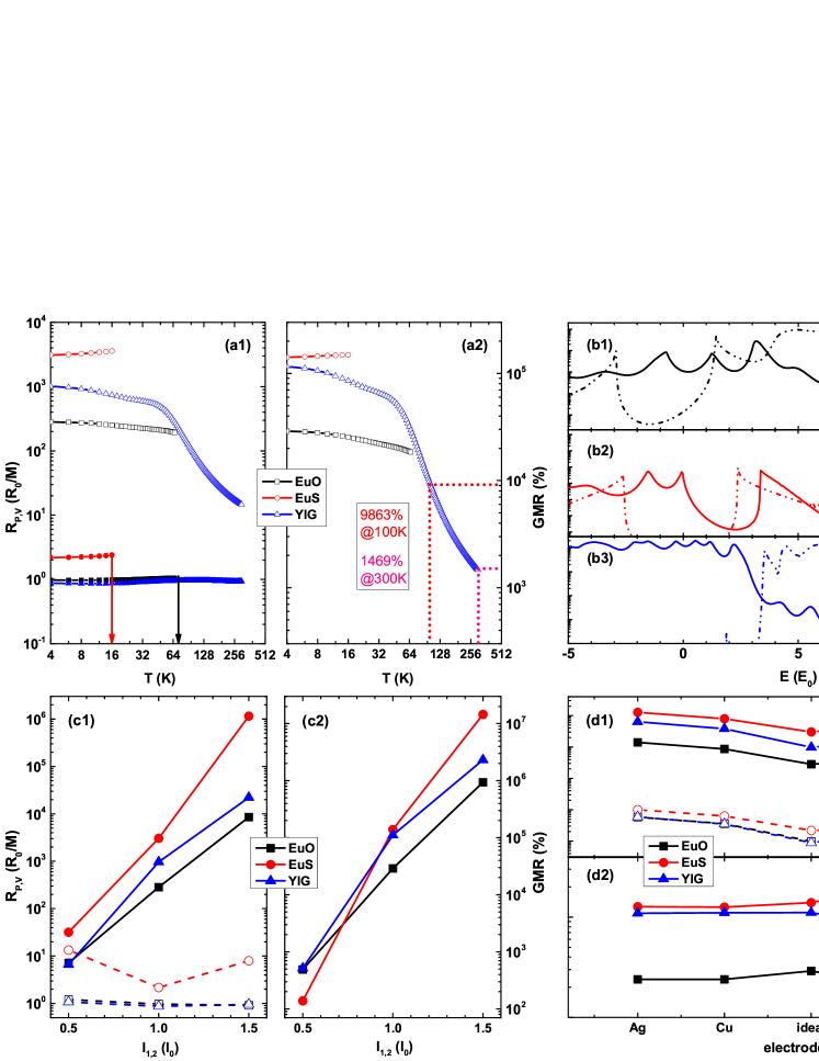
Application at high temperature is crucial. Fig. 5(a) shows , , and GMR as a function of temperature. The temperature range is limited to , for which the ferromagnetisms hold and the inelastic scattering can be ignored. It is seen that, for all ferromagnets increase slightly as the temperature, while shows a complicated dependence. It decreases with temperature for EuO and YIG and increases for EuS. Accordingly, the GMR for EuS/EuO/YIG follows an increasing/decreasing/decreasing behavior, with a value of // observed at 16K/68K/100K. For YIG the Curie temperature is higher than room temperature. A large GMR of is evaluated at 300K by ignoring the inelastic scattering not . These values imply promising high temperature or even room temperature GMR for EuO and YIG.
Due to Eq. (2), spin current at a finite temperature is determined by the zero-temperature ones in an energy range . In Fig. 5(b), we plot the latter for the three magnets and two configurations. It can be seen that, the () conductance for all magnets (EuS) reaches almost the maximum around the Fermi energy. As a result, the higher the temperature, the smaller (bigger) the finite temperature spin current (MR). The cases become opposite for the V configuration of EuO and YIG, because the spin current reaches almost the local minimum at the Fermi energy. The different energy bands are responsible for these different temperature dependences.
Fig. 5(c) shows the dependence of , , and GMR on the magnet length. It is found that, changes slightly with the magnet length while increases exponentially. When the length increase from 1 to 1.5 (still within the ballistic regime), the GMR increases to , , for EuO, EuS, and YIG, respectively. This is as large as the extraordinary magnetoresistance in semiconductor-metal hybrid systems Solin et al. (2000); Hewett and Kusmartsev (2010). For the V configuration, electrons transport evanescently in the second magnet. Due to an imaginary wave vector in the term , this leads a behavior of and . Due to this behavior, the negative temperature dependence (see Fig. 5 (a)) for YIG and EuO can be counteracted, and a huge room temperature GMR is expectable for YIG. Asymmetric spin valves with short left and long right magnets are suggested to enhance the GMR within the ballistic regime.
In all the above calculations, the effect of electrodes is ignored. Such an ideal contact can be achieved by specific metals with special distance to graphene (e.g., Au/Cu/Ag at 3.2/3.4/3.7) Giovannetti et al. (2008). Fig. 5(d) shows the calculated results for several familiar metal electrodes at their equilibrium distances. For Ag, Cu, Au, and Pt, respectively Giovannetti et al. (2008), which are rather smaller than the proximity induced doping’s. It is observed that, no matter for which magnets and for which configurations, the MR increases as the electrode becomes non ideal; the heavier the contact doping, the larger the MR increases. This is because the symmetric pristine-ferromagnetism (insulating)-pristine structure for the left (right) magnets becomes asymmetric doped-ferromagnetism-pristine or pristine-insulating-doped ones. However, the GMR can show different behaviors. It increases for EuS with positive doping (Au and Pt) and for YIG with negative doping (Cu and Ag), while decreases for EuO with any doping and for EuS (YIG) with negative (positive) doping. These results suggest that, the proposed GMR is rather robust to familiar metallic contacts, and can be even enhanced for YIG and EuS with proper contacts.
In summary, we have proposed a distinguished GMR that is magnetic field-free, vertically configured, and magnetism-tunable. The proximity effect and electric field effect in a novel graphene spin valve, both stemming from the 2D nature of graphene, play a central role. Outstanding performances such as huge values at high temperature ( at 68K and 100K), exponential enhancement by magnet length, and robustness to familiar electrodes have been demonstrated. These results may offer a viable path to a magnetic field-free spintronics as well as an evidence for the magnetisms. The uniform Hamiltonian constructed in the sublattice space can be applied to investigate spin transport in related nanostructures. Since the spin Dirac gaps increases as fewer layer Hallal et al. (2017), larger GMR is predicted in graphene grown on thinner substrates. We encourage experimental researches on the proposed GMR and mechanisms.
This work was supported by the National Natural Science Foundation of China (NSFC) under Grant No. 11404300, the Science Challenge Project (SCP) under Grant No. TZ2016003-1, and the ST Innovation Fund of IEE, CAEP under Grant No. S20140807.
References
- Han et al. (2014) W. Han, R. K. Kawakami, M. Gmitra, and J. Fabian, Nature Nanotechnology 9, 794 (2014).
- Feng et al. (2017) Y. P. Feng, L. Shen, M. Yang, A. Wang, M. Zeng, Q. Wu, S. Chintalapati, and C.-R. Chang, Wiley Interdisciplinary Reviews: Computational Molecular Science (2017).
- Haugen et al. (2008) H. Haugen, D. Huertas-Hernando, and A. Brataas, Physical Review B 77, 115406 (2008).
- Yang et al. (2013) H.-X. Yang, A. Hallal, D. Terrade, X. Waintal, S. Roche, and M. Chshiev, Physical Review Letters 110, 046603 (2013).
- Hallal et al. (2017) A. Hallal, F. Ibrahim, H. Yang, S. Roche, and M. Chshiev, 2D Materials (2017).
- Song and Dai (2015) Y. Song and G. Dai, Applied Physics Letters 106, 223104 (2015).
- Ang et al. (2016) Y. S. Ang, L. Ang, C. Zhang, and Z. Ma, Physical Review B 93, 041422 (2016).
- Su et al. (2017) S. Su, Y. Barlas, J. Li, J. Shi, and R. K. Lake, Physical Review B 95, 075418 (2017).
- Swartz et al. (2012) A. G. Swartz, P. M. Odenthal, Y. Hao, R. S. Ruoff, and R. K. Kawakami, ACS Nano 6, 10063 (2012).
- Swartz et al. (2013) A. G. Swartz, K. M. McCreary, W. Han, J. J. Wong, P. M. Odenthal, H. Wen, J.-R. Chen, R. K. Kawakami, Y. Hao, R. S. Ruoff, et al., Journal of Vacuum Science & Technology B, Nanotechnology and Microelectronics: Materials, Processing, Measurement, and Phenomena 31, 04D105 (2013).
- Wang et al. (2015) Z. Wang, C. Tang, R. Sachs, Y. Barlas, and J. Shi, Physical Review Letters 114, 016603 (2015).
- Mendes et al. (2015) J. Mendes, O. A. Santos, L. Meireles, R. Lacerda, L. Vilela-Leão, F. Machado, R. Rodríguez-Suárez, A. Azevedo, and S. Rezende, Physical Review Letters 115, 226601 (2015).
- Leutenantsmeyer et al. (2016) J. C. Leutenantsmeyer, A. A. Kaverzin, M. Wojtaszek, and B. J. van Wees, 2D Materials 4, 014001 (2016).
- Evelt et al. (2017) M. Evelt, H. Ochoa, O. Dzyapko, V. E. Demidov, A. Yurgens, J. Sun, Y. Tserkovnyak, V. Bessonov, A. B. Rinkevich, and S. O. Demokritov, Physical Review B 95, 024408 (2017).
- Wei et al. (2016) P. Wei, S. Lee, F. Lemaitre, L. Pinel, D. Cutaia, W. Cha, F. Katmis, Y. Zhu, D. Heiman, J. Hone, et al., Nature Materials (2016).
- Novoselov et al. (2004) K. S. Novoselov, A. K. Geim, S. V. Morozov, D. Jiang, Y. Zhang, S. V. Dubonos, I. V. Grigorieva, and A. A. Firsov, Science 306, 666 (2004).
- Kim et al. (2012) S. Kim, I. Jo, D. Dillen, D. Ferrer, B. Fallahazad, Z. Yao, S. Banerjee, and E. Tutuc, Physical Review Letters 108, 116404 (2012).
- Baibich et al. (1988) M. N. Baibich, J. M. Broto, A. Fert, F. N. Van Dau, F. Petroff, P. Etienne, G. Creuzet, A. Friederich, and J. Chazelas, Physical Review Letters 61, 2472 (1988).
- Hwang and Cheong (1997) H. Hwang and S.-W. Cheong, Science 278, 1607 (1997).
- Cheianov and Fal ko (2006) V. V. Cheianov and V. I. Fal ko, Physical Review B 74, 041403 (2006).
- McCann et al. (2006) E. McCann, K. Kechedzhi, V. I. Fal ko, H. Suzuura, T. Ando, and B. Altshuler, Physical Review Letters 97, 146805 (2006).
- Zhai and Chang (2008) F. Zhai and K. Chang, Physical Review B 77, 113409 (2008).
- Kim and Kim (2008) W. Y. Kim and K. S. Kim, Nature Nanotechnology 3, 408 (2008).
- Muñoz-Rojas et al. (2009) F. Muñoz-Rojas, J. Fernández-Rossier, and J. Palacios, Physical Review Letters 102, 136810 (2009).
- Zhang et al. (2010) Y.-T. Zhang, H. Jiang, Q.-F. Sun, and X. Xie, Physical Review B 81, 165404 (2010).
- Lu et al. (2011) J. Lu, H. Zhang, W. Shi, Z. Wang, Y. Zheng, T. Zhang, N. Wang, Z. Tang, and P. Sheng, Nano Letters 11, 2973 (2011).
- Bai et al. (2010) J. Bai, R. Cheng, F. Xiu, L. Liao, M. Wang, A. Shailos, K. L. Wang, Y. Huang, and X. Duan, Nature Nanotechnology 5, 655 (2010).
- Friedman et al. (2010) A. L. Friedman, J. L. Tedesco, P. M. Campbell, J. C. Culbertson, E. Aifer, F. K. Perkins, R. L. Myers-Ward, J. K. Hite, C. R. Eddy Jr, G. G. Jernigan, et al., Nano Letters 10, 3962 (2010).
- Liao et al. (2012) Z.-M. Liao, H.-C. Wu, S. Kumar, G. S. Duesberg, Y.-B. Zhou, G. L. Cross, I. V. Shvets, and D.-P. Yu, Advanced Materials 24, 1862 (2012).
- Gopinadhan et al. (2015) K. Gopinadhan, Y. J. Shin, R. Jalil, T. Venkatesan, A. K. Geim, A. H. C. Neto, and H. Yang, Nature Communications 6 (2015).
- Kisslinger et al. (2015) F. Kisslinger, C. Ott, C. Heide, E. Kampert, B. Butz, E. Spiecker, S. Shallcross, and H. B. Weber, Nature Physics 11, 650 (2015).
- Zhai and Wang (2016) M.-X. Zhai and X.-F. Wang, Scientific Reports 6 (2016).
- Wu et al. (2017) H.-C. Wu, A. N. Chaika, M.-C. Hsu, T.-W. Huang, M. Abid, M. Abid, V. Y. Aristov, O. V. Molodtsova, S. V. Babenkov, Y. Niu, et al., Nature Communications 8 (2017).
- El-Ahmar et al. (2017) S. El-Ahmar, W. Koczorowski, A. Poźniak, P. Kuświk, W. Strupiński, and R. Czajka, Applied Physics Letters 110, 043503 (2017).
- (35) Here, is several times of to ensure that the edge effect is negligible.
- Zollner et al. (2016) K. Zollner, M. Gmitra, T. Frank, and J. Fabian, Physical Review B 94, 155441 (2016).
- Song and Wu (2013) Y. Song and H.-C. Wu, Journal of Physics: Condensed Matter 25, 355301 (2013).
- Song et al. (2012) Y. Song, H.-C. Wu, and Y. Guo, Applied Physics Letters 100, 253116 (2012).
- Song et al. (2013) Y. Song, F. Zhai, and Y. Guo, Applied Physics Letters 103, 183111 (2013).
- Born and Wolf (1980) M. Born and E. Wolf, Principles of optics: electromagnetic theory of propagation, interference and diffraction of light (Elsevier, 1980).
- Morozov et al. (2008) S. Morozov, K. Novoselov, M. Katsnelson, F. Schedin, D. Elias, J. A. Jaszczak, and A. Geim, Physical Review Letters 100, 016602 (2008).
- Chen et al. (2008) J.-H. Chen, C. Jang, S. Xiao, M. Ishigami, and M. S. Fuhrer, Nature Nanotechnology 3, 206 (2008).
- Büttiker et al. (1985) M. Büttiker, Y. Imry, R. Landauer, and S. Pinhas, Physical Review B 31, 6207 (1985).
- (44) Note, this value would be smaller when taking into account the scattering.
- Solin et al. (2000) S. Solin, T. Thio, D. Hines, and J. Heremans, Science 289, 1530 (2000).
- Hewett and Kusmartsev (2010) T. H. Hewett and F. Kusmartsev, Physical Review B 82, 212404 (2010).
- Giovannetti et al. (2008) G. Giovannetti, P. Khomyakov, G. Brocks, V. v. Karpan, J. Van den Brink, and P. Kelly, Physical Review Letters 101, 026803 (2008).