Complete photonic bandgaps in supercell photonic crystals
Abstract
We develop a class of supercell photonic crystals supporting complete photonic bandgaps based on breaking spatial symmetries of the underlying primitive photonic crystal. One member of this class based on a two-dimensional honeycomb structure supports a complete bandgap for an index-contrast ratio as low as , making this the first such 2D photonic crystal to support a complete bandgap in lossless materials at visible frequencies. The complete bandgaps found in such supercell photonic crystals do not necessarily monotonically increase as the index-contrast in the system is increased, disproving a long-held conjecture of complete bandgaps in photonic crystals.
Since their discovery, photonic crystals have become an indispensable technology across the entire field of optical physics due to their ability to confine and control light of an arbitrary wavelength Yablonovitch (1987); John (1987); Joannopoulos et al. (1997, 2011). This critical feature is achieved by designing the crystal lattice to possess a complete photonic bandgap, a range of frequencies for which no light can propagate regardless of its momentum or polarization. Unlike their electronic counterparts in conventional crystals, whose band structure is limited to the crystal lattices available in atomic and molecular structures, the dielectric structure comprising a photonic crystal can be specified with nearly complete arbitrariness, yielding a vast design space for optimizing photonic crystals for specific applications that is limited only by the index of refraction of available materials at the operational wavelength. For example, photonic crystals have been developed to promote absorption in monolayer materials Piper and Fan (2014); Piper et al. (2014), or for use in achieving high-power solid-state lasers Noda et al. (2001); Kurosaka et al. (2010); Hirose et al. (2014). Moreover, this design freedom in dielectric structures has been leveraged in numerous studies to optimize the complete bandgaps in high-index materials Fan et al. (1994); Dobson and Cox (1999); Doosje et al. (2000); Cox and Dobson (2000); Johnson and Joannopoulos (2000); Shen et al. (2002); Biswas et al. (2002); Maldovan et al. (2002, 2003); Michielsen and Kole (2003); Sigmund and Jensen (2003); Toader et al. (2003); Jensen and Sigmund (2004); Stanley et al. (2004); Kao et al. (2005); Maldovan and Thomas (2005); Halkjær et al. (2006); Watanabe et al. (2006); Sigmund and Hougaard (2008); Men et al. (2010); Jia and Thomas (2011); Liang and Johnson (2013). Unfortunately, similar efforts to realize new crystal structures or improve upon existing ones to achieve complete bandgaps in low-index materials have yielded only minor improvements upon traditional simple crystal structures with high symmetry Oskooi et al. (2009); Men et al. (2014), i.e. the inverse triangular lattice in two-dimensions Joannopoulos et al. (2011) and the network diamond lattice in three-dimensions Maldovan and Thomas (2004). This has led many to conclude that the known high-symmetry dielectric structures are nearly optimal for achieving low-index complete bandgaps Men et al. (2014).
However, the ability to realize complete bandgaps for low-index materials is critically important to the development of many photonics technologies operating in the visible wavelength range, such as augmented and virtual reality systems, where the highest index lossless materials have –. Currently, there are no known 2D photonic crystals which display a complete bandgap in this index contrast regime, and thus it is not possible to realize dual-polarization in-plane guiding at this index contrast using photonic crystal slabs. Although a few 3D photonic crystals do display a complete bandgap in this range, 3D photonic crystals are difficult to fabricate Yablonovitch (1993); Lin et al. (1998); Noda et al. (2000); Vlasov et al. (2001); Qi et al. (2004).
In this Letter, we demonstrate a new class of complete photonic bandgaps which are achieved by judiciously breaking symmetry, rather than promoting it. By starting with a photonic crystal possessing a large bandgap for one polarization, we show that by expanding the primitive cell of the photonic crystal to form a supercell and then slightly adjusting the dielectric structure within this supercell to break part of the translational symmetry of the original primitive cell, a bandgap in the other polarization can be opened, thus producing a complete bandgap. This method yields a two-dimensional photonic crystal based on a honeycomb lattice with a complete bandgap that persists down to an index-contrast ratio of , the lowest known index-contrast ratio in 2D photonic crystals. Such low index contrast bandgaps can also be translated into photonic crystal slabs, where they represent the first structures able to confine optical frequencies in-plane regardless of their polarization. In contrast to the complete photonic bandgaps found in traditional photonic crystals, complete bandgaps in supercell photonic crystals do not necessarily monotonically increase as a function of the index-contrast ratio, disproving a long-held conjecture in the photonic crystal literature Joannopoulos et al. (2011).
To illuminate how symmetry breaking can help to realize complete photonic bandgaps, we first consider the 2D photonic crystal comprised of a network structure on a honeycomb lattice depicted in Fig. 1(a). The primitive cell of this system contains a pair of vertices in this network lattice, and the system can be parameterized solely in terms of the thickness, , of the lines forming the network structure. Although in a low-index network structure, , a wide range of yields a large transverse electric (TE) bandgap as shown in Fig. 1(b), no complete photonic bandgap exists for any choice of for this choice of .
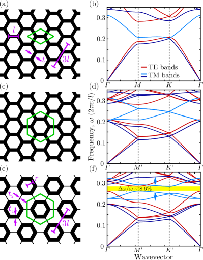
However, starting from the crystal structure as shown in Fig. 1(a), we can find a complete bandgap in a closely related supercell photonic crystal. First, we increase the size of the primitive cell to contain six vertices which form the supercell, as depicted in Fig. 1(c). In doing so, each of the bands in the primitive Brillouin zone fold up into three bands in the supercell Brillouin zone, shown in Fig. 1(d). Along the edge of the supercell Brillouin zone (), pairs of the folded supercell bands can form lines of degeneracies, i.e. degenerate contours Cerjan et al. (2016), and one such degenerate contour is formed per trio of folded bands originating from the same band in the primitive Brillouin zone. From the perspective of the supercell photonic crystal, the degeneracies comprising each of the degenerate contours are accidental, and are only the result of the supercell obeying an extra set of spatial symmetries as it is a three-fold copy of the original photonic crystal. Thus by breaking these symmetries, the degeneracies forming the degenerate contours are lifted, and a gap can begin to open between the two transverse magnetic (TM) bands. The supercell is now characterized in terms of three parameters, the thickness of the center lines, , the thickness of the connecting lines, , and the size of the thick-lined hexagons, , shown in Fig. 1(e). When the symmetry breaking becomes sufficiently strong, a complete photonic bandgap opens between the th and th bands of the system, whose maximum width at can be found numerically to be . Here, is the difference between the minimum of the th band and the maximum of the th band, while is the central frequency between the two bands. Rigorously, after the symmetry of this system is broken, the supercell containing six vertices becomes the primitive cell of the system. However, for semantic convenience, we will continue to refer to this larger primitive cell as the ‘supercell’ and reserve ‘primitive cell’ for the smaller system whose symmetry is intact.
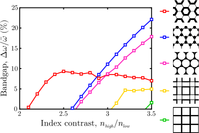
Previously, the lowest index-contrast ratio known to support a complete bandgap in a 2D photonic crystal was a decorated honeycomb lattice, shown as the blue curve in Fig. 2, which has a complete bandgap between the rd and th bands for index-contrast ratios as low as Oskooi et al. (2009). This structure provides a relatively modest improvement upon the traditional triangular lattice of air holes, also shown in Fig. 2 as the pink curve. In contrast, the supercell honeycomb lattice possesses a complete bandgap for index-contrast ratios as low as , and as such is the first 2D photonic crystal design that can realize a complete bandgap for visible wavelengths where the largest index of refraction possible in lossless materials is –, which is found in Diamond Phillip and Taft (1964), Titanium Dioxide DeVore (1951), and Strontium Titanate Weber (1994). Furthermore, this supercell honeycomb structure could also be used in conjunction with high-index materials available in other frequency ranges so that the low-index material used in the structure need not be air. For example, this could enable realizing complete bandgaps in completely solid photonic crystal fibers operating in the communications band, where the high index regions are Silicon, , and the low-index regions are filled with fused silica, , such that for m.
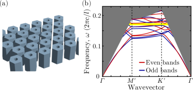
This 2D supercell honeycomb structure can also be used to design new photonic crystal slabs so as to provide confinement in three dimensions. In Fig. 3, we show a supercell honeycomb slab with a complete below-light-line dual-polarization bandgap of for . Note that in photonic crystal slabs, to define a band gap one only considers the phase space regions below the light line, as above the light line the radiations modes form a continuum with no gaps. To the best of our knowledge, this represents the first system which could confine visible frequencies emitted from a omni-polarization source burried within the system. Likewise, this design could also be used to realize entirely solid photonic crystal slabs for communications frequencies where higher index dielectric materials are available.
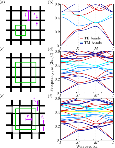
The procedure used above is not restricted to the honeycomb lattice. To illustrate this point, we use the same method to produce a complete bandgap in a 2D supercell square network lattice, as shown in Fig. 4. Unlike in the primitive honeycomb crystal, the TE bandgap in the underlying primitive square lattice is spanned by two TM bands. Thus, a complete bandgap is only realized for sufficiently strong symmetry breaking so that not only does a gap open in each degenerate contour of the folded supercell TM bands, but that a gap opens between these two folded bands. This limits the overall width of the complete bandgap, and the lowest index-contrast ratio for which this structure possesses a complete bandgap is , as shown as the yellow line in Fig. 2. However, this still represents a significant improvement upon the range of index-contrast ratios which can yield a complete bandgap when compared against other 2D photonic crystals based on a square lattice.
Complete bandgaps in supercell photonic crystal possess three features which distinguish them from complete bandgaps found in traditional photonic crystals. First, as noted above, these structures have been designed by specifically breaking symmetry within the system. This is entirely distinct from what is observed for bandgaps found in traditionally designed structures, which consider the high-symmetry triangular lattice in 2D and diamond lattice in 3D to be near optimal. Second, as can be seen in Fig. 2, complete bandgaps in supercell structures do not necessarily monotonically increase in size as a function of the index-contrast. This disproves a long-held conjecture of complete bandgaps in photonic crystals, that the optimized bandgap (between the same two bands) always increases as the index contrast increases Joannopoulos et al. (2011). Finally, the complete bandgap in supercell crystals is found between higher order bands. This is unlike many photonic crystal structures previously considered where the complete bandgap occurs between lower-order bands.
Designing two-dimensional supercell photonic crystals to possess complete bandgaps has three steps. First, a candidate primitive photonic crystal must be constructed which possesses a large bandgap for one polarization, and which is spanned by at most one or two bands in the other polarization. Second, a supercell must be generated from this primitive cell such that the degenerate contours of the folded band spanning the single-polarization bandgap lie entirely within the single-polarization bandgap. Finally, the supercell perturbation which breaks the underlying primitive cell symmetries must be designed, such that a bandgap in the degenerate contour opens before the single-polarization bandgap in the original primitive system closes.
We expect these same design principles to hold for finding complete bandgaps in three-dimensional supercell photonic crystals, but in practice we have been unable to find such a structure. Although the second and third steps in the above procedure are relatively straightforward, finding good candidate primitive cell structures is much more challenging in 3D, as it is rare to find what would be a large bandgap spanned by only a single other band. For comparison, this is relatively easy in 2D, structures with isolated dielectric elements typically possess large TM bandgaps, but not TE bandgaps, while network structures typically possess large TE bandgaps, but no TM bandgaps.
In conclusion, we have developed a new class of photonic crystals which support complete bandgaps which stem from breaking spatial symmetries. These structures can exhibit complete bandgaps for much lower index-contrast ratios than was previously known, enabling the confinement of visible light in two-dimensional structures. The discovery of this new class of supercell structures also provides encouragement that there may be significant improvements remaining to be discovered in designing and optimizing complete bandgaps at low index-contrasts in both two- and three-dimensional systems.
Acknowledgements.
This work was supported by an AFOSR MURI program (Grant No. FA9550-12-1-0471), and an AFOSR project (Grant No. FA9550-16-1-0010).References
- Yablonovitch (1987) E. Yablonovitch, Phys. Rev. Lett. 58, 2059 (1987).
- John (1987) S. John, Phys. Rev. Lett. 58, 2486 (1987).
- Joannopoulos et al. (1997) J. D. Joannopoulos, P. R. Villeneuve, and S. Fan, Nature 386, 143 (1997).
- Joannopoulos et al. (2011) J. D. Joannopoulos, S. G. Johnson, J. N. Winn, and R. D. Meade, Photonic Crystals: Molding the Flow of Light (Second Edition) (Princeton University Press, 2011).
- Piper and Fan (2014) J. R. Piper and S. Fan, ACS Photonics 1, 347 (2014).
- Piper et al. (2014) J. R. Piper, V. Liu, and S. Fan, Appl. Phys. Lett. 104, 251110 (2014).
- Noda et al. (2001) S. Noda, M. Yokoyama, M. Imada, A. Chutinan, and M. Mochizuki, Science 293, 1123 (2001).
- Kurosaka et al. (2010) Y. Kurosaka, S. Iwahashi, Y. Liang, K. Sakai, E. Miyai, W. Kunishi, D. Ohnishi, and S. Noda, Nat Photon 4, 447 (2010).
- Hirose et al. (2014) K. Hirose, Y. Liang, Y. Kurosaka, A. Watanabe, T. Sugiyama, and S. Noda, Nat Photon 8, 406 (2014).
- Fan et al. (1994) S. Fan, P. R. Villeneuve, R. D. Meade, and J. D. Joannopoulos, Appl. Phys. Lett. 65, 1466 (1994).
- Dobson and Cox (1999) D. Dobson and S. Cox, SIAM J. Appl. Math. 59, 2108 (1999).
- Doosje et al. (2000) M. Doosje, B. J. Hoenders, and J. Knoester, J. Opt. Soc. Am. B 17, 600 (2000).
- Cox and Dobson (2000) S. J. Cox and D. C. Dobson, J. Comput. Phys. 158, 214 (2000).
- Johnson and Joannopoulos (2000) S. G. Johnson and J. D. Joannopoulos, Appl. Phys. Lett. 77, 3490 (2000).
- Shen et al. (2002) L. Shen, S. He, and S. Xiao, Phys. Rev. B 66, 165315 (2002).
- Biswas et al. (2002) R. Biswas, M. Sigalas, K. Ho, and S. Lin, Phys. Rev. B 65, 205121 (2002).
- Maldovan et al. (2002) M. Maldovan, A. Urbas, N. Yufa, W. Carter, and E. Thomas, Phys. Rev. B 65, 165123 (2002).
- Maldovan et al. (2003) M. Maldovan, C. K. Ullal, W. C. Carter, and E. L. Thomas, Nat Mater 2, 664 (2003).
- Michielsen and Kole (2003) K. Michielsen and J. S. Kole, Phys. Rev. B 68, 115107 (2003).
- Sigmund and Jensen (2003) O. Sigmund and J. S. Jensen, Philos. Trans. R. Soc. A 361, 1001 (2003).
- Toader et al. (2003) O. Toader, M. Berciu, and S. John, Phys. Rev. Lett. 90, 233901 (2003).
- Jensen and Sigmund (2004) J. S. Jensen and O. Sigmund, Appl. Phys. Lett. 84, 2022 (2004).
- Stanley et al. (2004) M. B. Stanley, S. J. Osher, and E. Yablonovitch, IEICE Trans. Electron. 87, 258 (2004).
- Kao et al. (2005) C. Y. Kao, S. Osher, and E. Yablonovitch, Appl. Phys. B 81, 235 (2005).
- Maldovan and Thomas (2005) M. Maldovan and E. L. Thomas, J. Opt. Soc. Am. B 22, 466 (2005).
- Halkjær et al. (2006) S. Halkjær, O. Sigmund, and J. S. Jensen, Struct. Multidiscip. Optim. 32, 263 (2006).
- Watanabe et al. (2006) Y. Watanabe, Y. Sugimoto, N. Ikeda, N. Ozaki, A. Mizutani, Y. Takata, Y. Kitagawa, and K. Asakawa, Opt. Express 14, 9502 (2006).
- Sigmund and Hougaard (2008) O. Sigmund and K. Hougaard, Phys. Rev. Lett. 100, 153904 (2008).
- Men et al. (2010) H. Men, N. C. Nguyen, R. M. Freund, P. A. Parrilo, and J. Peraire, Journal of Computational Physics 229, 3706 (2010).
- Jia and Thomas (2011) L. Jia and E. L. Thomas, Phys. Rev. A 84, 033810 (2011).
- Liang and Johnson (2013) X. Liang and S. G. Johnson, Opt. Express 21, 30812 (2013).
- Oskooi et al. (2009) A. F. Oskooi, J. D. Joannopoulos, and S. G. Johnson, Opt. Express 17, 10082 (2009).
- Men et al. (2014) H. Men, K. Y. K. Lee, R. M. Freund, J. Peraire, and S. G. Johnson, Opt. Express 22, 22632 (2014).
- Maldovan and Thomas (2004) M. Maldovan and E. L. Thomas, Nat Mater 3, 593 (2004).
- Yablonovitch (1993) E. Yablonovitch, J. Opt. Soc. Am. B 10, 283 (1993).
- Lin et al. (1998) S. Y. Lin, J. G. Fleming, D. L. Hetherington, B. K. Smith, R. Biswas, K. M. Ho, M. M. Sigalas, W. Zubrzycki, S. R. Kurtz, and J. Bur, Nature 394, 251 (1998).
- Noda et al. (2000) S. Noda, K. Tomoda, N. Yamamoto, and A. Chutinan, Science 289, 604 (2000).
- Vlasov et al. (2001) Y. A. Vlasov, X.-Z. Bo, J. C. Sturm, and D. J. Norris, Nature 414, 289 (2001).
- Qi et al. (2004) M. Qi, E. Lidorikis, P. T. Rakich, S. G. Johnson, J. D. Joannopoulos, E. P. Ippen, and H. I. Smith, Nature 429, 538 (2004).
- Johnson and Joannopoulos (2001) S. G. Johnson and J. D. Joannopoulos, Opt. Express 8, 173 (2001).
- Cerjan et al. (2016) A. Cerjan, A. Raman, and S. Fan, Phys. Rev. Lett. 116, 203902 (2016).
- Phillip and Taft (1964) H. R. Phillip and E. A. Taft, Phys. Rev. 136, A1445 (1964).
- DeVore (1951) J. R. DeVore, J. Opt. Soc. Am. 41, 416 (1951).
- Weber (1994) M. J. Weber, CRC Handbook of Laser Science and Technology Supplement 2: Optical Materials (CRC Press, 1994).