Proximity Eliashberg theory of electrostatic field-effect-doping in superconducting films
Abstract
We calculate the effect of a static electric field on the critical temperature of a s-wave one band superconductor in the framework of proximity effect Eliashberg theory. In the weak electrostatic field limit the theory has no free parameters while, in general, the only free parameter is the thickness of the surface layer where the electric field acts. We conclude that the best situation for increasing the critical temperature is to have a very thin film of a superconducting material with a strong increase of electron-phonon (boson) constant upon charging.
pacs:
74.45.+c, 74.62.-c,74.20.FgI INTRODUCTION
In the last decade, electric double layer (EDL) gating has come to the forefront of solid state physics due to its capability to tune the surface carrier density of a wide range of different materials well beyond the limits imposed by solid-gate field-effect devices. The order-of-magnitude enhancement in the gate electric field allows this technique to reach doping levels comparable to those of standard chemical doping. This is possible due to the extremely large specific capacitance of the EDL that builds up at the interface between the electrolyte and the material under study FujimotoReview2013 ; UenoReview2014 ; GoldmanReview2014 ; SaitoReview2016 .
EDL gating was first exploited to control the surface electronic properties of relatively low-carrier density systems, where the electric field effect is more readily observable. Field-induced superconductivity was first demonstrated in strontium titanate UenoNatureMater2008 and zirconium nitride chloride YeNatureMater2010 ; SaitoScience2015 , and subsequently on other insulating systems such as perovskites UenoNatureNano2011 and layered transition-metal dichalcogenides YeScience2012 ; JoNanoLett2015 ; LuScience2015 ; ShiSciRep2015 ; YuNatNano2015 ; CostanzoNatNano2016 ; SaitoNatPhys2016 . Significant effort was also invested in the control of the superconducting properties of cuprates bollinger11 ; LengPRL2011 ; LengPRL2012 ; MaruyamaAPL2015 ; JinSciRep2016 ; FeteAPL2016 ; BurlachkovPRB1993 ; GhinovkerPRB1995 ; walter16 , although in this class of materials the mechanism behind the carrier density modulation is still debated walter16 .
More recently however, several experimental studies have been devoted to the exploration of field effect in superconductors libro with a large ( cm-3) native carrier density. The interplay between two different ground states, namely superconductivity and charge density waves, was explored in titanium and niobium diselenides LiNature2016 ; YoshidaAPL2016 ; XiPRL2016 . The thickness and gate voltage dependence of a high-temperature superconducting phase were studied in iron selenide, both in thin-film ShiogaiNaturePhys2015 and thin flake LeiPRL2016 ; HanzawaPNAS2016 forms. The effect of the ultrahigh interface electric fields achievable via EDL gating were also probed in standard BCS superconductors, namely niobium ChoiAPL2014 and niobium nitride PiattiJSNM2016 ; PiattiNbN .
With the exception of the work of Ref.XiPRL2016, on niobium diselenide, all of these studies have been performed on relatively thick samples ( nm) with a thickness larger than the electrostatic screening length. These systems are thus expected to develop a strong dependence of their electronic properties along the direction (z being perpendicular to the sample surface). As a first approximation, this dependence can be conceptualized by schematizing the system as the parallel of a surface layer (where the carrier density is modified by the electric field) and an unperturbed bulk. The two electronic systems can be expected to couple via superconducting proximity effect, resulting in a complicated response to the applied electric field that goes well beyond a simple modification of the superconducting properties of the surface layer alone PiattiNbN and is strongly dependent on both the electrostatic screening length and the total thickness of the film.
So far, the only quantitative assessment of this phenomenon has been reported in the framework of the strong-coupling limit of the BCS theory of superconductivity PiattiNbN . A proper theoretical treatment for field effect on more complex materials, which can be described only by means of the more complete Eliashberg theory carbibastardo ; ummarinorev , is lacking. Given the rising interest in the control of the properties of superconductors by means of surface electric fields, the development of such a theoretical approach would be very convenient not only to quantitatively describe the results of future experiments, but also to determine beforehand the experimental conditions (e.g., device thickness) most suitable for an optimal control of the superconducting order via electric fields.
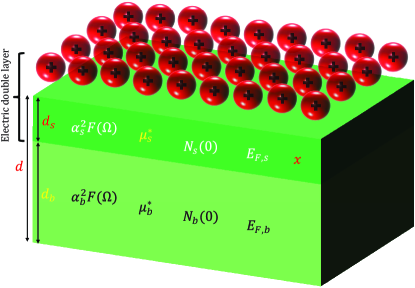
In this work, we use the Eliashberg theory of proximity effect to describe a junction composed by the perturbed surface layer (), where the carrier density is modulated (with a doping level per unitary cell ), and the underlying unperturbed bulk (). Here and indicate “surface” and “bulk” respectively (see Fig. 1). Under the application of an electric field, and the material behaves like a junction between a superconductor and a normal metal in the temperature range bounded by and . If the application of the electric field increases (decreases) , then the surface layer will be the superconductor (normal metal) and the bulk will be the normal metal (superconductor). We perform the calculation for lead since all the input parameters of the theory are well-known in the literature for this strong-coupling superconductor carbibastardo .
II MODEL: PROXIMITY ELIASHBERG EQUATIONS
In general, a proximity effect at a superconductor/normal metal junction is observed as the opening of a finite superconducting gap in the normal metal together with its reduction in a thin region of the superconductor close to the junction. In our model we use the one band s-wave Eliashberg equations carbibastardo ; ummarinorev with proximity effect to calculate the critical temperature of the system. In this case we have to solve four coupled equations for the gaps and the renormalization functions , where are the Matsubara frequencies. The imaginary-axis equations with proximity effect Mc ; Carbi1 ; Carbi2 ; Carbi3 ; kresin are:
| (1) |
| (2) |
| (3) |
| (4) |
where are the Coulomb pseudopotentials in the surface and in the bulk respectively, is the Heaviside function and is a cutoff energy at least three times larger than the maximum phonon energy. Thus we have
| (5) |
| (6) |
and thus ,
| (7) |
and
| (8) |
where are the electron-phonon spectral functions, is the junction cross-sectional area, the transmission matrix equal to one in our case because the material is the same, and are the surface and bulk layer thicknesses respectively, such that ( where is the total film thickness) and are the densities of states at the Fermi level for the surface and bulk material. The electron-phonon coupling constants are defined as
and the representative energies as
The solution of these equations requires eleven input parameters: the two electron-phonon spectral fuctions , the two Coulomb pseudopotentials , the values of the normal density of states at the Fermi level , the shift of the Fermi energy that enters in the calculation of the surface Coulomb pseudopotential (as shown later), the value of the surface layer , the film thickness and the junction cross-sectional area . The values of and are experimental data. The exact value of , in particular in the case of very strong electric fields at the surface of a thin film, is in general difficult to determine a priori PiattiNbN . Thus, we leave it as a free parameter of the model, and we perform our calculations for different reasonable estimations of its value.
Typically, the bulk values of , , and are known and can be found in the literature. Thus, we assume that we need to determine only their surface values. In the next Section, we will use density functional theory (DFT) to calculate , and .
The value of the Coulomb pseudopotential in the surface layer can be obtained in the following way: in the Thomas-Fermi theory where the dielectric function is UmmaC60 and the bare Coulomb pseudopotential is the angular average of the screened electrostatic potential
| (9) |
Since Morel it turns out that
| (10) |
Hence we write
| (11) |
with . Since can be calculated by numerically solving Eq. 13, and by remembering that the square of Thomas-Fermi wave number is proportional to , we have
| (12) |
and thus
| (13) |
The new Coulomb pseudopotential Morel in the surface layer is thus
| (14) |
We note that, usually, the effect of electrostatic doping on is very small and can be neglected. We can quantify the effect on of this small modulation of by computing it in the case of maximum doping and very thin film ( nm), i.e. when the effect is largest. As discussed in the next Section, the unperturbed Coulomb pseudopotential is , while for the maximum doping Eqs. 12-16 give . If we use we find respectively K for the bulk (unperturbed) value of the Coulomb pseudopotential and K for the surface value of the Coulomb pseudopotential. Thus, if we consider the Coulomb pseudopotential to be doping-independent we underestimate the critical temperature of a K ( percent).
However, a possible critical situation can appear when the applied electric field is very strong and the Thomas-Fermi approximation does not hold anymore. In such a case, becomes ill-defined as the Thomas-Fermi dielectric function is no longer strictly valid for very large electric fields. Nevertheless, the true dielectric function should still be a function of the ratio pastore , which in the free-electron model is independent on the normal density of states at the Fermi level. Thus, Eq. 9 should still be able to describe the behavior of the system as a first approximation.
III CALCULATION OF , and
DFT calculations are performed within the mixed-basis pseudopotential method (MBPP) meyer . For lead a norm-conserving relativistic pseudopotential including semicore states and partial core corrections is constructed following the prescription of Vanderbilt vanderbilt . This provides both scalar-relativistic and spin-orbit components of the pseudopotential. Spin-orbit coupling (SOC) is then taken into account within each DFT self-consistency cycle (for more details on the SOC implementation see heid10 ). The MBPP approach utilizes a combination of local functions and plane waves for the basis set expansion of the valence states, which reduces the size of the basis set significantly. One type local function is added at each lead atomic site to efficiently treat the deep potential. Sufficient convergence is then achieved with a cutoff energy of 20 Ry for the plane waves. The exchange-correlation it treated in the local density approximation (LDA) hedin . Brillouin zone (BZ) integrations are performed on regular k-point meshes in conjuction with a Gaussian broadening of eV. For phonons, meshes are used, while for the calculations of density of states and electron-phonon coupling (EPC) even denser meshes are employed.
Phonon properties are calculated with the density-functional perturbation theory baroni ; zein as implemented in the MBPP approach heid99 , which also provides direct access to the electron-phonon coupling matrix elements. The procedure to extract the Eliashberg function is outlined in Ref. heid10 . Dynamical matrices and corresponding EPC matrix elements are obtained on a phonon mesh. These quantities are then interpolated using standard Fourier techniques to the whole BZ, and the Eliashberg functions are calculated by integration over the BZ using the tetrahedron method on a mesh. SOC is consistently taken into account in all calculations including lattice dynamical and EPC properties. It is well known from previous work, that SOC is necessary for a correct quantitative description of both the phonon anomalies and EPC of undoped bulk lead heid10 .
Charge induction is simulated by adding an appropriate number of electrons during the DFT self-consistency cycle, compensated by a homogeneous background charge to retain overall charge neutrality. Electronic structure properties and the Eliashberg function are calculated for face centred cubic (fcc) lead with the lattice constant Å as obtained by optimization for the undoped case. For doping levels considered here, we found that to a good approximation charge induction does not change the band structure but merely results in a shift of . In a previous study, the variation of the EPC was studied as function of the averaging energy sklyadneva . The present approach goes beyond this analysis by taking into account explicitly the effect of charge induction on the screening properties, which modifies both the phonon spectrum and the EPC matrix elements.
Finally we point out that, since this DFT approach simulates the effect of the electric field by adding extra charge carriers to the system together with a uniform compensating counter-charge (Jellium model Pines ) is unable to describe inhomogeneous distributions caused by the screening of the electric field itself. A more complete approach has been developed in Ref. Brumme, , and requires the self-consistent solution of the Poisson equation; however, this method is currently unable to compute the phonon spectrum of the gated material, making it unsuitable for the application of the proximity Eliashberg formalism.
IV RESULTS AND DISCUSSION
We start our calculations by fixing the input parameters for bulk lead according to the established literature. We set to its experimental value carbibastardo K. The undoped gives a corresponding electron-phonon coupling . Assuming a cutoff energy meV and a maximum energy meV in the Eliashberg equations, we are thus able to determine the bulk Coulomb pseudopotential to be to obtain the exact experimental critical temperature .
| 0.000 | 1.5612 | 4.8431 | 0.25866 | 0.00 | 0.14164 | 7.2200 |
| 0.075 | 1.5582 | 4.8432 | 0.25754 | 108.42 | 0.14136 | 7.2197 |
| 0.150 | 1.6137 | 4.7176 | 0.25611 | 218.77 | 0.14116 | 7.3165 |
| 0.300 | 2.0237 | 4.2175 | 0.26770 | 435.07 | 0.14074 | 8.2862 |
| 0.400 | 2.5392 | 3.5668 | 0.27833 | 571.62 | 0.14048 | 8.9406 |
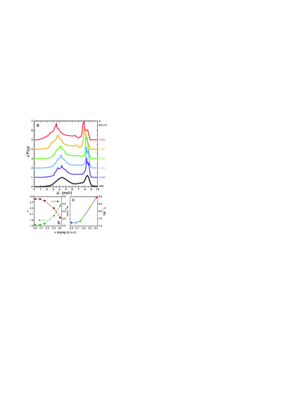
In Fig. 2a we show the calculated electron-phonon spectral functions resulting at the increase of the doping level . Specifically, we plot the curves corresponding to e-/unit cell. We calculate the spectral functions until cell because for larger values of doping an instability emerges in the calculation processes. We can see the phonon softening evidenced by a reduction of with increasing doping level. The increase of the carrier density gives rise to two competing effects: the value of (i.e. the representative phonon energy) decreases while the value of electron-phonon coupling costant increases (see Fig. 2b). Since the critical temperature is an increasing function of both and , in general this could result in either a net enhancement or suppression of , depending on which of the two contributions is dominant. Consequently the ideal situation for obtaining largest critical temperature in an electric field doped material is to have a strong increase of and concurrently. In the case of lead the contribution from the increase of is dominant over that from the reduction of , giving rise to a net increase of the superconducting critical temperature (as we report in Fig. 2c). In addition, in Table 1 we summarize all the input parameters of the proximity Eliashberg equations as obtained from the DFT calculations.
Having determined the response of the superconducting properties of a homogeneous lead film to a modulation of its carrier density, we can now consider the behavior of the more realistic junction between the perturbed surface layer and the unperturbed bulk. In order to do so, however, it is now mandatory to select a value for the thickness of the perturbed surface layer. Close to , the superfluid density is small HirschPRB2004 and the screening is dominated by unpaired electrons. Thus, a very rough approximation would be to set to the Thomas-Fermi screening length , which for lead can be estimated to be 0.15 nm Basavaiah . However, we have recently shown PiattiNbN that this assumption might not be satisfactory in the presence of the very large electric fields that build up in the electric double layer. Indeed, our experimental findings on niobium nitride indicated that the screening length increases for very large doping values PiattiNbN . However, it is reasonable to assume the exact entity of this increase to be specific to each material. Thus, while the qualitative behavior can be expected to be general, the exact values of determined for niobium nitride cannot be directly applied to lead.
In order not to lose the generality of our approach, we calculate the behavior of our system for three different choices of the behavior of . We start by expressing , where is a dimensionless parameter indicating how much expands beyond the Thomas-Fermi value for large doping levels, and is the specific doping value upon which this increase in takes place. By selecting , we allow the upper half of our doping values to go beyond the Thomas-Fermi approximation. We then perform proximity-coupled Eliashberg calculations for and five different film thicknesses nm, always assuming the junction area to be m2. Note that the case of course corresponds to the case where the material satisfies the Thomas-Fermi model for any value of doping: in this case, the model has no free parameters.
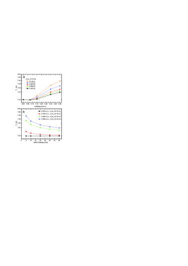
In Fig. 3 we plot the evolution of upon increasing electron doping and assuming that the Thomas-Fermi model always holds ( and ), for different values of film thickness. The calculations show that the qualitative increase in with increasing doping level that we observed in the homogeneous case is retained also in proximized films of any thinckess (see Fig. 3a). However, the presence of a coupling between surface and bulk induced by the proximity effect gives rise to a key difference with respect to the homogeneous case, namely, a strong dependence of on film thickness in the doped films. Indeed, the magnitude of the shift with respect to the homogeneous case is heavily suppressed already in films as thin as nm. This behavior is best seen in Fig. 3b, where we plot the same data as a function of the total film thickness for all doping levels. As we can see the increase of critical temperature drops dramatically with increasing film thickness. We have not calculated the critical temperature for monolayer films since the approximations of the model would no longer apply in this case: in particular the unperturbed electron-phonon spectral function would have been different from the bulk-like one we employed in our calculations Pratappone .
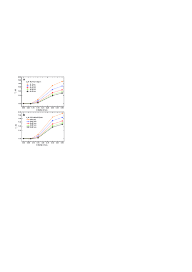
We now consider the effect of the different degrees of confinement for the induced charge carriers at the surface of the films. We do so by allowing the perturbed surface layer to spread further in the depth of the film for large electron doping, i.e. by increasing the parameter in the definition of . In Fig. 4 we plot the evolution of with increasing electron doping and for different film thicknesses, in the two cases ( is allowed to expand up to nm) and ( is allowed to expand up to nm). We can first observe how a different value of does not change the qualitative behavior of the films. The evolution of with increasing electron doping is still comparable to both the homogeneous case and the proximized films in the Thomas-Fermi limit. The suppression of the increase with increasing film thickness is also similar to the latter case. However, the magnitude of the shift for the same values of film thickness and doping level per unit cell is clearly the more enhanced the larger the value of . This is to be expected, as larger values of increase the fraction of the film that is perturbed by the application of the electric field and reduce the shift dampening operated by the proximity effect. In principle, for values of large enough (or film thickness small enough) one could reach the limit value and recover the homogeneous case where the shift is maximum.
All the calculations we performed so far assumed that one could directly control the induced carrier density per unit volume, , in the surface layer, without an explicit upper limit. However, this is not an experimentally achievable goal in a field-effect device architecture. In this class of devices, the polarization of the gate electrode allows one to tune the electric field at the interface and thus the induced carrier density per unit surface, , required to screen it, i.e. within our model is distributed within a layer of thickness . In general, the determination of the exact depth profile of this distribution requires the self-consistent solution of the Poisson equation Brumme ; however, as a first approximation we can consider this distribution to be constant, obtaining an effective doping level per unit volume simply as . This procedure allows one to employ the same DFT-Eliashberg formalism we developed before in order to simulate a field effect experiment on a superconducting thin film.
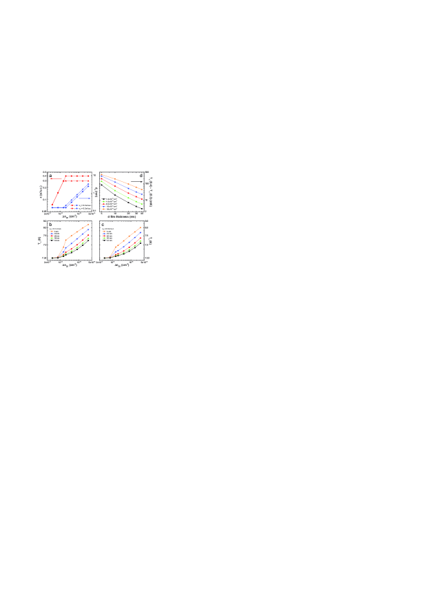
In addition, in the previous calculations we supposed that can only take on two values as a function of , depending on the threshold value . When we consider the field-effect architecture, however, the parameters and in the expression are no longer independent as in the previous case. Moreover, according to our recent experimental findings on niobium nitride PiattiNbN , is a monotonically increasing function of . We include this behavior in our calculations in the following way: Once the maximum doping level is selected, is automatically determined by the requirement for any . Fig. 5a shows the resulting dependence of the doping per unit volume and surface layer thickness on the induced carrier density per unit surface , for two different values of the maximum doping level and e-/unit cell. When is small enough so that , the Thomas-Fermi screening holds, is constant and linearly increases with . As soon as becomes large enough that is constant (), the Thomas-Fermi screening is no longer valid and increases linearly with .
In Fig. 5b and 5c we plot the resulting modulation of for five different film thicknesses in the cases and e-/unit cell respectively. In both cases we can readily distinguish between two regimes of . When , Thomas-Fermi screening holds and we reproduce the behavior we observed in Fig. 3a. In this regime, the induced carrier density directly modulates and thus the electron-phonon spectral function . The modulation is thus a result of a direct modification of the material properties at the surface, with proximity effect simply operating a “smoothing” the larger the value of the film thickness. On the other hand, when , the surface properties () are no longer modified by the extra charge carriers, and the further modulation of originates entirely from the proximity effect as determined by the increase in .
We can also compare the shifts for different maximum doping levels . Fig. 5d shows the difference between the corresponding to and e-/unit cell as a function of the total film thickness, for different values of . We can clearly see how is always larger for the films with larger , for any value of film thickness, even if the associated values of are always smaller. This indicates that the maximum achievable value of is dominant with respect to the increase of to determine the final value of , also in the doping regime .
Of course, in a real sample we don’t expect the transition between the two regimes to be so clear-cut, as the saturation of to would occur over a finite range of . In this intermediate region, the modulation of and would both contribute in a comparable way to the final value of in the film. We stress, however, that in both regimes the proximity effect is fundamental in determining the of the gated film. We also note that the proximized Eliashberg equations are able to account for a non-uniform scaling of the shift for different values of film thickness, unlike the models that use approximated analytical equations for .
V CONCLUSIONS
In this work, we have developed a general method for the theoretical simulation of field-effect-doping in superconducting thin films of arbitrary thickness, and we have benchmarked it on lead as a standard strong-coupling superconductor. Our method relies on ab-initio DFT calculations to compute how the increasing doping level per unit volume modifies the structural and electronic properties of the material (shift of Fermi level , density of states , and electron-phonon spectral function ). The Coulomb pseudopotential is determined by simple calculations from some of these parameters. The properties of the pristine thin film (critical temperature , device area and total film thickness ) can be obtained either from the literature or experimentally from standard transport measurements. For doping values where the Thomas-Fermi theory of screening is satisfied, the perturbed surface layer thickness is constant () and the theory has no free parameters.
Once all the input parameters are known, our method allows to compute the transition temperature for arbitrary values of film thickness and electron doping in the surface layer by solving the proximity-coupled Eliashberg equations in the surface layer and unperturbed bulk. On the other hand, if no reliable estimations of the surface layer thickness are available, our method allows one to determine by reproducing the experimentally-measured . This allows to probe deviations from the standard Thomas-Fermi theory of screening in the presence of very large interface electric fields.
We also show how, even in the case where the Thomas-Fermi approximation breaks down and the doping level can no longer be increased, the transition temperature of a thin film can still be indirectly modulated by the electric field by changing the surface layer thickness . For what concerns artificial enhancements of in superconducting thin films, we conclude that very thin films (, in order to minimize the smoothing operated by the proximity effect) of a superconductive material characterized by a strong increase of the electron-phonon (boson) coupling upon changing its carrier density are required to optimize the effectiveness of the field-effect-device architecture.
Finally, our calculations indicate that sizable enhancements of the order of K should be achievable in thin films of a standard strong-coupling superconductor such as lead, for easily realizable thicknesses of nm and doping levels routinely induced via EDL gating in metallic systems. These features may open the possibility for superconducting switchable devices and electrostatically reconfigurable superconducting circuits above liquid helium temperature.
Acknowledgements.
The work of G. A. U. was supported by the Competitiveness Program of NRNU MEPhI.References
- (1) T. Fujimoto and K. Awaga, Phys. Chem. Chem. Phys. 15, 8983 (2013)
- (2) K. Ueno, H. Shimotani, H. T. Yuan, J. T. Ye, M. Kawasaki, and Y. Iwasa, J. Phys. Soc. Jpn. 83, 032001 (2014)
- (3) A. M. Goldman, Annu. Rev. Mater. Res. 44, 45 (2014)
- (4) Y. Saito, T. Nojima, and Y. Iwasa, Supercond. Sci. Technol. 29, 093001 (2016)
- (5) K. Ueno, S. Nakamura, H. Shimotani, A. Ohtomo, N. Kimura, T. Nojima, H. Aoki, Y. Iwasa, and M. Kawasaki, Nat. Mater. 7, 855 (2008)
- (6) J. T. Ye, S. Inoue, K. Kobayashi, Y. Kasahara, H. T. Yuan, H. Shimotani, and Y. Iwasa, Nat. Mater. 9, 125 (2010)
- (7) Y. Saito, Y. Kasahara, J. T. Ye, Y. Iwasa, and T. Nojima, Science 350, 409 (2015)
- (8) K. Ueno, S. Nakamura, H. Shimotani, H. T. Yuan, N. Kimura, T. Nojima, H. Aoki, Y. Iwasa, and M. Kawasaki, Nat. Nanotech. 6, 408 (2011)
- (9) J. T. Ye, Y. J. Zhang, R. Akashi, M. S. Bahramy, R. Arita, and Y. Iwasa, Science 338, 1193 (2012)
- (10) S. Jo, D. Costanzo, H. Berger, and A. F. Morpurgo, Nano Lett. 15 1197 (2015)
- (11) J. M. Lu, O. Zheliuk, I. Leermakers, N. F. Q. Yuan, U. Zeitler, K. T. Law, and J. T. Ye, Science 350, 1353 (2015)
- (12) W. Shi, J. T. Ye, Y. Zhang, R. Suzuki, M. Yoshida, J. Miyazaki, N. Inoue, Y. Saito, and Y. Iwasa, Sci. Rep. 5, 12534 (2015)
- (13) Y. Yu, F. Yang, X. F. Lu, Y. J. Yan, Y.-H. Cho, L. Ma, X. Niu, S. Kim, Y.-W. Son, D. Feng, S. Li, S.-W. Cheong, X. H. Chen, and Y. Zhang, Nat. Nanotechnol. 10, 270 (2015)
- (14) D. Costanzo, S. Jo, H. Berger, and A. F. Morpurgo, Nat. Nanotechnol. 11, 399 (2016)
- (15) Y. Saito, Y. Nakamura, M. S. Bahramy, Y. Kohama, J. T. Ye, Y. Kasahara, Y. Nakagawa, M. Onga, M. Tokunaga, T. Nojima, Y. Yanase, and Y. Iwasa, Nat. Phys. 12, 144 (2016)
- (16) A. T. Bollinger, G. Dubuis, J. Yoon, D. Pavuna, J. Misewich, and I. Božović, Nature 472, 458 (2011)
- (17) X. Leng, J. Garcia-Barriocanal, S. Bose, Y. Lee, and A. M. Goldman, Phys. Rev. Lett. 107, 027001 (2011)
- (18) X. Leng, J. Garcia-Barriocanal, B. Yang, Y. Lee, J. Kinney, and A. M. Goldman, Phys. Rev. Lett. 108, 067004 (2012)
- (19) S. Maruyama, J. Shin, X. Zhang, R. Suchoski, S. Yasui, K. Jin, R. L. Greene, and I. Takeuchi, Appl. Phys. Lett. 107, 142602 (2015)
- (20) K. Jin, W. Hu, B. Zhu, J. Yuan, Y. Sun, T. Xiang, M. S. Fuhrer, I. Takeuchi, and R. L. Greene, Sci. Rep. 6, 26642 (2016)
- (21) A. Fête, L. Rossi, A. Augieri, and C. Senatore, Appl. Phys. Lett. 109, 192601 (2016)
- (22) L. Burlachkov, I. B. Khalfin, and B. Ya. Shapiro, Phys. Rev. B 48, 1156 (1993)
- (23) M. Ghinovker, V. B. Sandomirsky, and B. Ya. Shapiro, Phys. Rev. B 51, 8404 (1995)
- (24) J. Walter, H. Wang, B. Luo, C. D. Frisbie, and C. Leighton, ACS Nano 10, 7799 (2016)
- (25) P. Lipavsky, J. Kolacek, K. Morawetz, E. H. Brandt, and T.-J. Yang, Bernoulli Potential in Superconductors How the Electrostatic Field Helps to Understand Superconductivity, Lect. Notes Phys. 733, Springer, Berlin Heidelberg (2008)
- (26) L. J. Li, E. C. T. O’Farrell, K. P. Loh, G. Eda, B. Özyilmaz, and A. H. Castro Neto, Nature 529, 185 (2016)
- (27) M. Yoshida, J. T. Ye, T. Nishizaki, N. Kobayashi, and Y. Iwasa, Appl. Phys. Lett. 108, 202602 (2016)
- (28) X. X. Xi, H. Berger, L. Forró, J. Shan, and K. F. Mak, Phys. Rev. Lett. 117, 106801 (2016)
- (29) J. Shiogai, Y. Ito, T. Mitsuhashi, T. Nojima, and A. Tsukazaki, Nat. Phys. 12, 42 (2016)
- (30) B. Lei, J. H. Cui, Z. J. Xiang, C. Shang, N. Z. Wang, G. J. Ye, X. G. Luo, T. Wu, Z. Sun, and X. H. Chen, Phys. Rev. Lett. 116, 077002 (2016)
- (31) K. Hanzawa, H. Sato, H. Hiramatsu, T. Kamiya, and H. Hosono, Proc. Natl. Acad. Sci. USA 113, 3986 (2016)
- (32) J. Choi, R. Pradheesh, H. Kim, H. Im, Y. Chong, and D. H. Chae, Appl. Phys. Lett 105, 012601 (2014)
- (33) E. Piatti, A. Sola, D. Daghero, G. A. Ummarino, F. Laviano, J. R. Nair, C. Gerbaldi, R. Cristiano, A. Casaburi, and R. S. Gonnelli, J. Supercond. Novel Magn. 29, 587 (2016)
- (34) E. Piatti, D. Daghero, G. A. Ummarino, F. Laviano, J. R. Nair, R. Cristiano, A. Casaburi, C. Portesi, A. Sola, and R. S. Gonnelli, Phys. Rev. B 95, 140501 (2017)
- (35) J. P. Carbotte, Rev. Mod. Phys. 62, 1027 (1990)
- (36) G. A. Ummarino, Eliashberg Theory. In: Emergent Phenomena in Correlated Matter, edited by E. Pavarini, E. Koch, and U. Schollwöck, Forschungszentrum Jülich GmbH and Institute for Advanced Simulations, pp.13.1-13.36 (2013) ISBN 978-3-89336-884-6
- (37) W.L. McMillan, Phys. Rev. 175, 537, (1968)
- (38) E. Schachinger and J. P. Carbotte, J. Low Temp. Phys. 54, 129 (1984)
- (39) H. G. Zarate and J. P. Carbotte, Phys. Rev. B 35, 3256, (1987)
- (40) H. G. Zarate and J. P. Carbotte, Physica B+ C 135, 203 (1985)
- (41) V. Z. Kresin, H. Morawitz, and S. A. Wolf, Mechanisms of Conventional and High Tc Superconductivity, Oxford University Press (1999)
- (42) G. A. Ummarino and R. S. Gonnelli, Phys. Rev. B 66, 104514 (2002)
- (43) P. Morel and P. W. Anderson, Phys. Rev. 125, 1263 (1962)
- (44) G. Grosso and G. Pastori Parravicini, Solid state Physics, Academic Press (2014), ISBN 9780123850300
- (45) G. Grimvall, The Electron-phonon Interaction in Metals, North Holland, Amsterdam (1981); G. A. Ummarino, Physica C 423, 96102 (2005)
- (46) F. Stern, Phys. Rev. Lett. 18, 546 (1967); E. Canel, M. P. Matthews, and R. K. P. Zia, Phys. Kondens. Mater. 15, 191 (1972); J. Lee and H. N. Spector, J. Appl. Phys. 54, 6989 (1983)
- (47) B. Meyer, C. Elsässer, and M. Fähnle, FORTRAN90 Program for Mixed-Basis Pseudopotential Calculations for Crystals, Max-Planck-Institut für Metallforschung, Stuttgart (unpublished)
- (48) D. Vanderbilt, Phys. Rev. B 32, 8412 (1985)
- (49) L. Hedin and B. I. Lundqvist, J. Phys. C 4, 2064 (1971)
- (50) R. Heid and K. P. Bohnen, Phys. Rev. B 60, R3709 (1999)
- (51) R. Heid, K.-P. Bohnen, I. Yu. Sklyadneva, and E. V. Chulkov, Phys. Rev. B 81, 174527 (2010)
- (52) S. Baroni, S. de Gironcoli, A. Dal Corso, and P. Giannozzi, Rev. Mod. Phys. 73, 515 (2001)
- (53) N. E. Zein, Fiz. Tverd. Tela (Leningrad) 26, 3028 (1984); N. E. Zein, Sov. Phys. Solid State 26, 1825 (1984)
- (54) I. Yu. Sklyadneva, R. Heid, P. M. Echenique, K.-B. Bohnen, and E. V. Chulkov, Phys Rev. B 85, 155115 (2012)
- (55) D. Pines and P. Nozieres, The theory of quantum liquids, Benjamin, New York (1966)
- (56) S. Basavaiah, J. M. Eldridge, and J. Matisoo, J. of Appl. Phys. 45, 457 (1974)
- (57) S. Bose, C. Galande, S. P. Chockalingam, R. Banerjee, P. Raychaudhuri, and P. Ayyub, J. Phys.: Condens. Matter 21, 205702 (2009)
- (58) T. Brumme, M. Calandra, and F. Mauri, Phys Rev. B 91, 155436 (2012)
- (59) J. E. Hirsch, Phys. Rev. B 70, 226504 (2004)